EP1498962A2 - Organische elektrolumineszente Anzeigevorrichtung - Google Patents
Organische elektrolumineszente Anzeigevorrichtung Download PDFInfo
- Publication number
- EP1498962A2 EP1498962A2 EP04016602A EP04016602A EP1498962A2 EP 1498962 A2 EP1498962 A2 EP 1498962A2 EP 04016602 A EP04016602 A EP 04016602A EP 04016602 A EP04016602 A EP 04016602A EP 1498962 A2 EP1498962 A2 EP 1498962A2
- Authority
- EP
- European Patent Office
- Prior art keywords
- lacuna
- organic
- display panel
- sealing film
- functional layer
- Prior art date
- Legal status (The legal status is an assumption and is not a legal conclusion. Google has not performed a legal analysis and makes no representation as to the accuracy of the status listed.)
- Withdrawn
Links
Images




Classifications
-
- H—ELECTRICITY
- H10—SEMICONDUCTOR DEVICES; ELECTRIC SOLID-STATE DEVICES NOT OTHERWISE PROVIDED FOR
- H10K—ORGANIC ELECTRIC SOLID-STATE DEVICES
- H10K59/00—Integrated devices, or assemblies of multiple devices, comprising at least one organic light-emitting element covered by group H10K50/00
- H10K59/80—Constructional details
- H10K59/87—Passivation; Containers; Encapsulations
- H10K59/871—Self-supporting sealing arrangements
-
- H—ELECTRICITY
- H10—SEMICONDUCTOR DEVICES; ELECTRIC SOLID-STATE DEVICES NOT OTHERWISE PROVIDED FOR
- H10K—ORGANIC ELECTRIC SOLID-STATE DEVICES
- H10K50/00—Organic light-emitting devices
- H10K50/80—Constructional details
- H10K50/84—Passivation; Containers; Encapsulations
- H10K50/841—Self-supporting sealing arrangements
-
- H—ELECTRICITY
- H10—SEMICONDUCTOR DEVICES; ELECTRIC SOLID-STATE DEVICES NOT OTHERWISE PROVIDED FOR
- H10K—ORGANIC ELECTRIC SOLID-STATE DEVICES
- H10K59/00—Integrated devices, or assemblies of multiple devices, comprising at least one organic light-emitting element covered by group H10K50/00
- H10K59/10—OLED displays
- H10K59/17—Passive-matrix OLED displays
Definitions
- This invention relates to an organic electroluminescence display panel.
- Organic electroluminescence (hereafter called "organic EL”) display panels which employ an organic light-emitting material exhibiting electroluminescence properties as the light emission source, have been known in the art.
- a typical organic EL display panel includes an organic EL element formed on a display area of a transparent substrate.
- the organic EL element is made by stacking, in order, a transparent electrode, an organic functional layer containing an organic light-emitting material, and a metal electrode.
- Such organic EL element is sealed by a sealing film.
- the sealing film is made from an inorganic material having gas barrier properties, such as silicon oxynitride (SiON).
- SiON silicon oxynitride
- the sealing film blocks paths of intrusion of water molecules and similar into the organic EL element, and prevents formation of non-light-emitting areas called dark spots. The dark spots are indication of degradation of the organic EL element.
- Such sealing film is for example disclosed in Japanese Patent Kokai (Laid-open Publication) No. 8-111286.
- This inorganic sealing film is usually fabricated by plasma CVD or other film deposition methods.
- a high residual stress occurs in in-plane and other directions of the film.
- This residual stress acts on the multilayer structure below the sealing film, thereby deforming the multilayer structure.
- delamination occurs at interfaces, such as the interface between the electrode layer and the organic functional layer, where the adhesive force is weak.
- adhesive forces at the interface between an organic material layer and an inorganic material layer are weak compared with the adhesive forces at interfaces between two inorganic material layers.
- the adhesive force at the interface is weak.
- the organic functional layer is a laminate of layers made from low-molecular weight organic material, delamination occurs readily. When such delamination occurs, the organic EL element fails, and a non-emissive portion is formed.
- an improved organic electroluminescence display panel includes a substrate, a first electrode layer formed on the substrate, an organic functional layer covering the first electrode layer, a second electrode layer provided on the organic functional layer, and a sealing layer covering the second electrode layer.
- the organic functional layer has one or more lacuna portions.
- the lacuna portion(s) can enhance adhesion between the sealing film and the substrate. Consequently even if the area over which the organic functional layer is formed is large, deformation of the sealing film does not occur readily, and so delamination of the laminate does not occur.
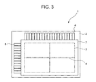
- an organic EL display panel 1 includes a substrate 2 of glass, resin, or other transparent material.
- the substrate 2 has a display area 3.
- Anode lines 4 which are first electrodes are formed in the display area 3.
- the anode lines 4 are formed from indium tin oxide (ITO) or another conductive material.
- An organic functional layer 5 is formed in the display area 3 so as to cover the anode lines 4.
- the organic functional layer 5 includes a light-emitting layer (not shown) of an organic light-emitting material having electroluminescence properties. It should be noted that the organic functional layer 5 may also include a functional layer (not shown) to enhance the efficiency of transport or injection of electrons or holes into the light-emitting layer.
- the cathode lines 6 are of aluminum (Al) or another conductive material.
- the laminate of the above described lines and layer(s) is sealed by a sealing film 7 which covers the cathode lines 6.
- the sealing film 7 is of a material such as silicon nitride having gas barrier properties.
- the organic functional layer 5 has a lacuna portion 8.
- the lacuna portion 8 may be a hole which penetrates the organic functional layer 5. Alternatively, the lacuna portion 8 may extend in a gap between adjacent electrodes 4. In the lacuna portion 8, the sealing film 7 is bonded to the substrate 2 through the anode 4.
- the organic functional layer 5 has the lacuna portion 8
- bonding between the sealing film 7 and substrate 2 is enhanced. Therefore, deformation of the sealing film covering the organic functional layer does not occur readily. Consequently it is possible to prevent the occurrence of delamination even if concentration of stress occurs at interfaces between the layers.
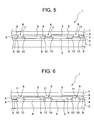
- the organic EL display panel 1 may have an insulating film 11 on the anode line electrodes 4.
- the insulating film 11 has (or defines) pixel windows 10.
- the pixel windows 10 demarcate light-emission areas 9 on the anode line electrodes 4.
- the insulating layer 11 may be made from silicon oxide, silicon nitride, silicon oxynitride, or other insulating material. Alternatively, the insulating layer 11 may be made from a polyimide or other polymer.
- the organic functional layer 5 is formed on this insulating layer 11, and the lacuna portion 8 of the organic functional layer 5 is formed at a position other than the pixel windows 10.
- the cathode lines 6 are formed on the organic functional layer 5.
- the cathode lines 6 are bonded to the insulating layer 11 in the lacuna portion 8.
- the sealing film 7 is formed so as to cover the cathode lines 6.
- the cathode lines 6 serve as an adhesive layer to improve the adhesion between the sealing film 7 and the insulating layer 11.
- the cathode lines 6 are made from A1 because A1 adheres well to the insulating layer 11 and sealing film 7 and enhances the adhesion between the sealing film 7 and substrate 2.
- the cathode line 6 may not be formed in the lacuna portion 8.
- the sealing film 7 and insulating layer 11 may be in direct contact in the lacuna portion 8.
- the lacuna portion 8 may be a groove extending along the anode line 4 or cathode line 6. In the depth direction, the groove 8 may reach the anode line 4.
- the organic functional layer 5 may have two grooves 8 (i.e., the vertical and horizontal grooves 8) which intersect with each other. In the depth direction, the grooves 8 may reach the anode lines 4.
- the organic functional layer 5 may have lacuna portions 8 which extend in gaps between all the anode lines 4 and cathode lines 6.
- the lacuna portions 8 may be linked with each other.
- the organic functional layer 5 has lacuna portions 8 in areas other than light-emitting areas 9 so that the organic functional layer 5 is constituted by a plurality of islands.
- the organic functional layer 5 can be formed only in light-emitting areas 9.
- the adhesive area between the sealing film 7 and substrate 2 can be increased.
- even if water-induced degradation occurs in one light-emitting area the water cannot diffuse along the organic functional layer 5. Hence spreading of the degradation to neighboring pixels can be prevented.
- the organic functional layer 5 may have a plurality of holes 8 as the lacuna portions.
- the lacuna portions 8 may be uniformly distributed (arranged) in the organic functional layer 5.
- the sealing film 7 can be bonded uniformly to the substrate 2.
- the lacuna portions 8 are not limited to holes, and may be grooves or recesses.
- the lacuna portions 8 may be distributed unevenly in the organic functional layer 5. Four examples of such configuration are shown in Fig. 8 to Fig. 11, respectively.
- the lacuna portions 8 are concentrated in a center portion of the display area 3.
- the display area 3 matches the shape of the organic functional layer 5. This configuration can reduce (restrict) deformation of the sealing film 7 in the center portion of the display area 3. Delamination can be prevented even when the sealing film 7 itself tends to deform in the center portion.
- lacuna portions 8 are concentrated along the periphery of the display area 3. These lacuna portions 8 are particularly useful to prevent deformation of the sealing film 7 near the periphery of the display area 3.
- the lacuna portions 8 are concentrated near the corners of the sealing film 7. This configuration is particularly effective when the sealing film 7 has a square or rectangular shape.
- the present invention is not limited to the above described and illustrated embodiment and modifications.
- the positions of the anode electrodes 4 and cathode electrodes 6 may be interchanged. That is, the cathode electrodes 6 are formed on the substrate 2, the organic functional layer 5 is formed on the cathode electrodes 6, and the anode electrodes 4 are formed on the organic functional layer 5.
- the anodes 4 and cathodes 6 are elongated electrode strips in the illustrated embodiment and modifications, this invention is not limited in this regard.
- either the anodes 4 or cathodes 6 alone may be the strip-shaped electrodes and the other may be a flat electrode.
- the organic EL display device 1 includes a plurality of strip-shaped anodes 4 and a single flat cathode 6. The flat cathode 6 is deposited over the entire surface. With such configuration, an active-type organic EL display panel can be manufactured.
Landscapes
- Physics & Mathematics (AREA)
- Optics & Photonics (AREA)
- Electroluminescent Light Sources (AREA)
Applications Claiming Priority (2)
| Application Number | Priority Date | Filing Date | Title |
|---|---|---|---|
| JP2003197547A JP4359091B2 (ja) | 2003-07-16 | 2003-07-16 | 有機エレクトロルミネセンス表示パネル |
| JP2003197547 | 2003-07-16 |
Publications (2)
| Publication Number | Publication Date |
|---|---|
| EP1498962A2 true EP1498962A2 (de) | 2005-01-19 |
| EP1498962A3 EP1498962A3 (de) | 2010-05-05 |
Family
ID=33475502
Family Applications (1)
| Application Number | Title | Priority Date | Filing Date |
|---|---|---|---|
| EP04016602A Withdrawn EP1498962A3 (de) | 2003-07-16 | 2004-07-14 | Organische elektrolumineszente Anzeigevorrichtung |
Country Status (4)
| Country | Link |
|---|---|
| US (1) | US20050012452A1 (de) |
| EP (1) | EP1498962A3 (de) |
| JP (1) | JP4359091B2 (de) |
| CN (1) | CN1578562A (de) |
Families Citing this family (6)
| Publication number | Priority date | Publication date | Assignee | Title |
|---|---|---|---|---|
| EP1724853B1 (de) * | 2005-05-17 | 2015-05-06 | LG Display Co., Ltd. | Organisches elektrolumineszentes Element |
| JP4701971B2 (ja) * | 2005-09-30 | 2011-06-15 | セイコーエプソン株式会社 | 表示装置および電子機器、表示装置の製造方法 |
| JP4466550B2 (ja) | 2005-12-08 | 2010-05-26 | ソニー株式会社 | 表示装置 |
| US8144140B2 (en) | 2007-06-13 | 2012-03-27 | Sony Corporation | Display apparatus and method of manufacturing the same |
| JP4884320B2 (ja) * | 2007-06-29 | 2012-02-29 | 京セラ株式会社 | 画像表示装置 |
| JP6371094B2 (ja) * | 2014-03-31 | 2018-08-08 | 株式会社ジャパンディスプレイ | 有機el表示装置 |
Family Cites Families (9)
| Publication number | Priority date | Publication date | Assignee | Title |
|---|---|---|---|---|
| JP4124379B2 (ja) * | 1995-08-08 | 2008-07-23 | パイオニア株式会社 | 有機エレクトロルミネセンス素子 |
| JP3539597B2 (ja) * | 1995-10-13 | 2004-07-07 | ソニー株式会社 | 有機光学的素子及びその製造方法 |
| JP3078257B2 (ja) * | 1998-04-15 | 2000-08-21 | ティーディーケイ株式会社 | 有機el表示装置及びその製造方法 |
| JP2000058270A (ja) * | 1998-08-04 | 2000-02-25 | Sony Corp | 光学素子および有機elディスプレイ |
| US6624570B1 (en) * | 1999-09-29 | 2003-09-23 | Sanyo Electric Co., Ltd. | Electroluminescent display device and method for its fabrication |
| JP2002252082A (ja) * | 2000-12-21 | 2002-09-06 | Sony Corp | 表示装置及び表示装置の製造方法 |
| JP3674848B2 (ja) * | 2001-10-31 | 2005-07-27 | 富士電機ホールディングス株式会社 | 有機薄膜発光ディスプレイ及びその製造方法 |
| JP2003234186A (ja) * | 2001-12-06 | 2003-08-22 | Sony Corp | 表示装置およびその製造方法 |
| JP2003187972A (ja) * | 2001-12-20 | 2003-07-04 | Dainippon Printing Co Ltd | 有機el素子の製造方法および有機el転写体と被転写体 |
-
2003
- 2003-07-16 JP JP2003197547A patent/JP4359091B2/ja not_active Expired - Lifetime
-
2004
- 2004-07-09 US US10/886,714 patent/US20050012452A1/en not_active Abandoned
- 2004-07-14 EP EP04016602A patent/EP1498962A3/de not_active Withdrawn
- 2004-07-16 CN CNA2004100709283A patent/CN1578562A/zh active Pending
Also Published As
| Publication number | Publication date |
|---|---|
| CN1578562A (zh) | 2005-02-09 |
| JP2005038633A (ja) | 2005-02-10 |
| EP1498962A3 (de) | 2010-05-05 |
| JP4359091B2 (ja) | 2009-11-04 |
| US20050012452A1 (en) | 2005-01-20 |
Similar Documents
| Publication | Publication Date | Title |
|---|---|---|
| US20250107323A1 (en) | Display device | |
| KR102424597B1 (ko) | 플렉서블 유기발광다이오드 표시장치 및 그 제조 방법 | |
| US6624572B1 (en) | Organic electroluminescence display panel and method for sealing the same | |
| US6664730B2 (en) | Electrode structure of el device | |
| TWI665799B (zh) | 有機電致發光元件構造、其製造方法及發光面板 | |
| KR20170135587A (ko) | 비표시 영역 상으로 연장하는 유기 발광층을 포함하는 유기 발광 표시 장치 | |
| US7872255B2 (en) | Organic light-emitting device | |
| US20090128030A1 (en) | Organic electroluminescence display device and manufacturing method thereof | |
| EP1643811A1 (de) | Organische elektrolumineszenz-display-tafel | |
| CN1638562A (zh) | 双面板型有机电致发光显示器件及其制造方法 | |
| KR100813833B1 (ko) | 전자 발광 소자와 그 제조방법 | |
| US20050062052A1 (en) | Panel of organic electroluminescent display | |
| KR102317715B1 (ko) | 유기 발광 표시 장치 및 그 제조 방법 | |
| EP1498962A2 (de) | Organische elektrolumineszente Anzeigevorrichtung | |
| EP1469518B1 (de) | Organische elektrolumineszente Anzeigevorrichtung und Herstellungsverfahren | |
| KR101694408B1 (ko) | 유기전계발광소자 및 그 제조방법 | |
| KR102656389B1 (ko) | 발광 소자를 포함하는 장치 | |
| KR101752318B1 (ko) | 유기전계 발광소자 제조 방법 | |
| KR102806921B1 (ko) | 표시 장치 | |
| CN111599935B (zh) | 一种柔性amoled面板封装结构及其封装方法 | |
| US20070007533A1 (en) | Pixel array strcuture | |
| JP2005259573A (ja) | 有機elパネルとその製造方法 | |
| JP2008153043A (ja) | エレクトロルミネッセンス装置及び電子機器 | |
| KR20160002537A (ko) | 유기전계발광 표시장치 | |
| KR100663083B1 (ko) | 방습 절연막을 구비하는 유기 전계 발광 디스플레이 패널및 그의 제조 방법 |
Legal Events
| Date | Code | Title | Description |
|---|---|---|---|
| PUAI | Public reference made under article 153(3) epc to a published international application that has entered the european phase |
Free format text: ORIGINAL CODE: 0009012 |
|
| AK | Designated contracting states |
Kind code of ref document: A2 Designated state(s): AT BE BG CH CY CZ DE DK EE ES FI FR GB GR HU IE IT LI LU MC NL PL PT RO SE SI SK TR |
|
| AX | Request for extension of the european patent |
Extension state: AL HR LT LV MK |
|
| PUAL | Search report despatched |
Free format text: ORIGINAL CODE: 0009013 |
|
| AK | Designated contracting states |
Kind code of ref document: A3 Designated state(s): AT BE BG CH CY CZ DE DK EE ES FI FR GB GR HU IE IT LI LU MC NL PL PT RO SE SI SK TR |
|
| AX | Request for extension of the european patent |
Extension state: AL HR LT LV MK |
|
| RAP1 | Party data changed (applicant data changed or rights of an application transferred) |
Owner name: PIONEER CORPORATION |
|
| AKY | No designation fees paid | ||
| STAA | Information on the status of an ep patent application or granted ep patent |
Free format text: STATUS: THE APPLICATION IS DEEMED TO BE WITHDRAWN |
|
| 18D | Application deemed to be withdrawn |
Effective date: 20101106 |