EP1495440B1 - Touch sensor with improved electrode pattern - Google Patents
Touch sensor with improved electrode pattern Download PDFInfo
- Publication number
- EP1495440B1 EP1495440B1 EP03726288A EP03726288A EP1495440B1 EP 1495440 B1 EP1495440 B1 EP 1495440B1 EP 03726288 A EP03726288 A EP 03726288A EP 03726288 A EP03726288 A EP 03726288A EP 1495440 B1 EP1495440 B1 EP 1495440B1
- Authority
- EP
- European Patent Office
- Prior art keywords
- touch sensor
- gaps
- touch
- junction
- gap
- Prior art date
- Legal status (The legal status is an assumption and is not a legal conclusion. Google has not performed a legal analysis and makes no representation as to the accuracy of the status listed.)
- Expired - Lifetime
Links
- 239000000758 substrate Substances 0.000 claims abstract description 22
- 230000005684 electric field Effects 0.000 claims abstract 3
- 239000011248 coating agent Substances 0.000 claims description 9
- 238000000576 coating method Methods 0.000 claims description 9
- 230000002093 peripheral effect Effects 0.000 claims description 7
- 238000012358 sourcing Methods 0.000 abstract description 31
- 230000037361 pathway Effects 0.000 abstract 1
- 230000005284 excitation Effects 0.000 description 13
- 238000013461 design Methods 0.000 description 12
- 238000005516 engineering process Methods 0.000 description 6
- 230000008901 benefit Effects 0.000 description 3
- 239000011521 glass Substances 0.000 description 3
- 238000005259 measurement Methods 0.000 description 3
- 239000000853 adhesive Substances 0.000 description 2
- 230000001070 adhesive effect Effects 0.000 description 2
- 238000013459 approach Methods 0.000 description 2
- 239000004020 conductor Substances 0.000 description 2
- 230000006872 improvement Effects 0.000 description 2
- 238000002347 injection Methods 0.000 description 2
- 239000007924 injection Substances 0.000 description 2
- 238000009413 insulation Methods 0.000 description 2
- 238000002955 isolation Methods 0.000 description 2
- 239000000463 material Substances 0.000 description 2
- 239000000523 sample Substances 0.000 description 2
- 230000009286 beneficial effect Effects 0.000 description 1
- 230000001413 cellular effect Effects 0.000 description 1
- 230000002860 competitive effect Effects 0.000 description 1
- 238000010276 construction Methods 0.000 description 1
- 230000003247 decreasing effect Effects 0.000 description 1
- 238000010586 diagram Methods 0.000 description 1
- 239000012212 insulator Substances 0.000 description 1
- 230000002452 interceptive effect Effects 0.000 description 1
- 238000000608 laser ablation Methods 0.000 description 1
- 230000000670 limiting effect Effects 0.000 description 1
- 239000004973 liquid crystal related substance Substances 0.000 description 1
- 238000004519 manufacturing process Methods 0.000 description 1
- 239000012528 membrane Substances 0.000 description 1
- 238000000034 method Methods 0.000 description 1
- 238000012986 modification Methods 0.000 description 1
- 230000004048 modification Effects 0.000 description 1
- 230000003071 parasitic effect Effects 0.000 description 1
- 239000004033 plastic Substances 0.000 description 1
- 230000008569 process Effects 0.000 description 1
- 238000012545 processing Methods 0.000 description 1
- 230000002829 reductive effect Effects 0.000 description 1
- 230000004044 response Effects 0.000 description 1
- 238000007650 screen-printing Methods 0.000 description 1
- 238000000926 separation method Methods 0.000 description 1
- 238000004088 simulation Methods 0.000 description 1
- 239000012780 transparent material Substances 0.000 description 1
Images


Classifications
-
- G—PHYSICS
- G06—COMPUTING; CALCULATING OR COUNTING
- G06F—ELECTRIC DIGITAL DATA PROCESSING
- G06F3/00—Input arrangements for transferring data to be processed into a form capable of being handled by the computer; Output arrangements for transferring data from processing unit to output unit, e.g. interface arrangements
- G06F3/01—Input arrangements or combined input and output arrangements for interaction between user and computer
- G06F3/03—Arrangements for converting the position or the displacement of a member into a coded form
- G06F3/041—Digitisers, e.g. for touch screens or touch pads, characterised by the transducing means
- G06F3/045—Digitisers, e.g. for touch screens or touch pads, characterised by the transducing means using resistive elements, e.g. a single continuous surface or two parallel surfaces put in contact
-
- G—PHYSICS
- G06—COMPUTING; CALCULATING OR COUNTING
- G06F—ELECTRIC DIGITAL DATA PROCESSING
- G06F2203/00—Indexing scheme relating to G06F3/00 - G06F3/048
- G06F2203/041—Indexing scheme relating to G06F3/041 - G06F3/045
- G06F2203/04113—Peripheral electrode pattern in resistive digitisers, i.e. electrodes at the periphery of the resistive sheet are shaped in patterns enhancing linearity of induced field
Definitions
- the field of the present invention relates to touch sensor technology, and more particularly to resistive and capacitive touch sensor technology.
- Touch sensors are transparent or opaque input devices for computers and other electronic systems. As the name suggests, touch sensors are activated by touch, either from a user's finger, or a stylus or some other device. Transparent touch sensors, and specifically touchscreens, are generally placed over display devices, such as cathode ray tube (CRT) monitors and liquid crystal displays, to create touch display systems. These systems are increasingly used in commercial applications such as restaurant order entry systems, industrial process control applications, interactive museum exhibits, public information kiosks, pagers, cellular phones, personal digital assistants, and video games.
- CTR cathode ray tube
- touch technology The dominant touch technologies presently in use are resistive, capacitive, infrared, and acoustic technologies. Touchscreens incorporating these technologies have delivered high standards of performance at competitive prices. All are transparent devices that respond to a touch by transmitting the touch position coordinates to a host computer. An important aspect of touchscreen performance is a close correspondence between true and measured touch positions at all locations within a touch sensitive area located on the touch sensor (i.e., the touch region).
- resistive touchscreen e.g., the AccuTouchTM product line of Elo TouchSystems, Inc. of Fremont, California
- a 5-wire resistive touchscreen e.g., the AccuTouchTM product line of Elo TouchSystems, Inc. of Fremont, California
- the glass substrate is coated with a resistive layer upon which voltage gradients are excited via electrode patterns that are disposed along the periphery of the substrate.
- associated electronics can sequentially excite gradients in both the X and Y directions, as described in U.S. Patent No. 3,591,718 .
- the underside of the coversheet has a conductive coating that provides electrical continuity between the touch location and voltage sensing electronics. Further details regarding 5-wire resistive touchscreens are found in U.S. Patent Nos. 4,220,815 , 4,661,655 , 4,731,508 , 4,822,957 , 5,045,644 , and 5,220,136 ..
- FIGs. 1 and 2 illustrate a touch screen substrate 2 in which respective X and Y excitations are produced on a touch region 4 by applying different corner voltages (in this case, 5 volts) to an electrode pattern 6 extending along the periphery 8 of the substrate 2.
- the arrows represent the direction of current flow across the touch region 4, and the dotted lines represent equipotential lines, i.e., lines along which the voltage is constant.
- the equipotential lines are perfectly straight lines, as suggested in Figs. 1 and 2 . Current flows perpendicular to these equipotential lines, so lines of current flow are straight when the equipotential lines are straight.
- an X excitation is generated by passing current through the touch region 4 injected at the right side of the border electrode pattern 6 and collected at the left side. That is, the left and right sides are in "sourcing” (or sinking) mode for the X excitation. Ideally, for X excitation, no current enters or exits the touch region 4 from the top and bottom sides. That is the top and bottom sides are "non-sourcing" for the X excitation.
- a Y excitation is generated by passing current through the touch region 4 injected at the top side of the border electrode pattern 6 and collected at the bottom side. That is, the top and bottom sides are in "sourcing” (or sinking) mode for the Y excitation.
- Y excitation no current enters or exits the touch region 4 from the left and right sides. That is, the left and right sides are "non-sourcing" for the Y excitation.
- Electronics can obtain touch information from a 5-wire resistive touchscreen via the voltage excitation described above, as well as current injection and capacitive architectures.
- a 9-wire connection scheme which provides drive and a sense line connections between the electronics and each of the four corner connection points, is also available.
- One 5-wire connection touch sensor utilizes peripheral electrode patterns with discrete overlap resistors, such as those found in Elo TouchSystems' AccuTouch TM products and disclosed in U.S. Patent No. 5,045,644 .
- peripheral electrode patterns with discrete overlap resistors such as those found in Elo TouchSystems' AccuTouch TM products and disclosed in U.S. Patent No. 5,045,644 .
- parallel resistive current paths are provided through gaps within isolation lines between peripheral electrode patterns on opposite sides of the touch region.
- the current paths produce an undesirable ripple non-linearity in the touch region near the peripheral electrode pattern.
- a finger moving across a straight line in this region will experience variations in the excitation voltage and hence variations in the measured coordinate (unless otherwise corrected for).
- the considerable ripple adjacent to the top and bottom resistor chains limits the accuracy of measurements in this area, and thus, the size of the effective touch region is therefore reduced.
- a higher density of electrical connections on the non-sourcing side tends to make matters worse.
- great linearity improvement on the sourcing sides is provided with a modest decrease in linearity on the non-sourcing sides. While this may appear to be quite a reasonable engineering trade-off, the marketplace is wary of anything that degrades any aspect of touchscreen performance.
- FIG. 3 shows a resistor chain 48 having Z-electrodes 50 with overlapping outer and inner portions 51, 52, the inner portions 52 of adjacent electrodes being closest at junctions 54.
- An array of insulating regions 55 having two gaps 56 for each overlap resistor electrode 50 runs parallel to the inner portions 52. Some of the gaps 56 are over the junctions 54.
- the V N and V N+1 equipotential lines tend to terminate on the electrodes 50, and all the equipotential lines in between V N and V N+1 bunch up at the junction 54, as illustrated in Fig. 5 .
- the resistor chain 48 of Fig. 3 will, in practice, have the equivalent circuit illustrated in Fig. 6 .
- US patent 6163313 on which the preamble of claim 1 is based, discloses a position touch sensor having a substrate and a resistive layer disposed on the substrate. At least one pair of electrodes is positioned on the resistive layer. A portion of one electrode is spaced from a portion of another electrode to produce an overlapped resistive region between the spaced portions of the electrodes. An insulating region extends into and terminates in the overlapped resistive region from a resistive region of the resistive layer outside the overlapped resistive region. There remains a need to improve the non-sourcing side linearity of touchscreens with discrete resistor structures.
- the present invention is directed to a touch sensor that utilizes electrically conductive islands in junction gaps in order to provide a true voltage divider within the gaps, thereby providing a linearly varying voltage sequence along the resistor chain.
- the touch sensor can be operated as a resistive touch sensor, e. g. , 5-or 9-wire, a capacitive touch sensor, or any touch sensor that requires series resistive chains.
- a touch sensor as claimed in any of the accompanying claims.
- a conductive island is located within a plurality of the junction gaps to provide maximum benefit.
- the non-junction gaps can be variously designed.
- a non-junction gap may be empty, i. e. , it contains no electrically conductive material.
- the non-junction gap may contain an extension from the inner portion of the electrode.
- the non-junction gap may contain a conductive island.
- the touchscreen system 100 generally comprises a touchscreen 105 (i.e., a touch sensor having a transparent substrate), controller electronics 110, and a display 120.
- the touchscreen system 100 is typically coupled to a host computer 115.
- the controller electronics 110 receives from the touchscreen 105 analog signals carrying touch information.
- the controller electronics 110 also sends to the touchscreen 105 excitation signals.
- the controller electronics 110 establishes a voltage gradient across the touchscreen 105. The voltages at the point of contact are representative of the position touched.
- the controller electronics 110 digitizes these voltages and transmits these digitized signals, or touch information in digital form based on these digitized signals, to the host computer 115 for processing.
- the touchscreen 105 comprises a gradient sheet 195 including a substrate 200 having a uniform resistive layer 205 permanently applied to one surface thereof.
- the resistive layer 205 further includes a touch region 206.
- the geometry of the substrate 200 may be, for example, planar (as shown in Fig. 8 ), or may be contoured to match the face of a curved object, such as a Cathode Ray Tube (CRT) face or other conventional video display screens.
- the substrate 200 can also have any perimeter configuration, e.g., rectangular (as shown), substantially rectangular, or circular.
- the substrate 200 and resistive layer 205 are preferably made of a substantially transparent material.
- the substrate 200 may be composed of an opaque material.
- a cover sheet 210 Spaced a small distance above the resistive layer 205 is a cover sheet 210, which is typically a flexible film 215 having a conductive coating 220 on the underside of the flexible film 215.
- the cover sheet 210 is joined to the remainder of the touchscreen 105 with an adhesive along its associated edges, or optionally, with an insulative adhesive frame 225 or the like.
- an electrode 230 connects the conductive coating 220 of the cover sheet 210 via lead 235 to appropriate external circuitry, such as the controller circuit 110.
- the conductive coating 220 attached to the cover sheet 210 is separated from the resistive layer 205 by a plurality of small transparent insulator islands or dots 240, which prevent accidental contact between the conductive coating 220 and the resistive layer 205.
- any conducting element such as a conducting stylus (not shown), can be used as an alternative.
- This conducting stylus may be used when the resistive layer 205 is sufficiently durable as to withstand damage from such contact.
- a capacitive or resistive pickup system can be used along with a user's finger or with an appropriate probe.
- a resistor chain 245 is spaced along each edge of the resistive layer 205 and is used for applying potentials to the resistive layer 205, so as to create orthogonal voltage gradients therein.
- the resistor chain 245 (composed of conductive regions, insulating regions, and resistive regions) includes discrete resistance units connected in series.
- the resistance values of the resistor chain 245 depend partly upon the resistive value of the resistive layer 205 that forms part of the resistor chain 245.
- the resistance values of the resistor chain 245 may vary in accordance with design requirements.
- There are four resistor chains 245 in the embodiment of Fig. 8 which are more specifically labeled 250, 255, 260, and 265.
- each resistor chain 250, 255, 260 or 265 are joined at or near the corners 270 of the resistive layer 205.
- Each of the corners 270 is provided with a respective one of the electrical leads 275, 280, 285, 290.
- the touchscreen 105 is connected to the controller electronics 110, which provides the voltage to the resistor chain 245 and processes information from the touchscreen 105.
- the conductive coating 220 of the cover sheet 210 makes direct electrical contact with the resistive layer 205 on the substrate 200.
- the cover sheet 210 can function as either a voltage sensing probe for sensing the voltage at the contacted area, or as a current injection source.
- the coversheet 210 may be replaced with a thin dielectric coating applied directly to resistive layer 205, in which case, the controller electronics 110 may support AC operation.
- the resistor chain 245 has Z-shaped electrodes 305, each having an outer portion 310 and an inner portion 315.
- the inner portion 315 of a first electrode 305 overlaps the outer portion 310 of a second, adjacent electrode 305.
- the resistive layer 205 (shown in Fig. 8 ) between these inner and outer portions forms a resistive connection 320.
- the inner portions 315 of adjacent electrodes 305 are separated from each other by junctions 325.
- a plurality of insulating regions 330 are formed in the gradient sheet 195 (shown in Fig. 8 ), for example, by removing the resistive layer 205 at selected places.
- gaps 335 are positioned between the inner portions 315 of the electrodes 305 and the touch region 206 (referred to as “non-junction gaps”) and some of the gaps 335 are positioned between the junctions 325 and the touch region 206 (referred to as “junction gaps").
- the insulating regions 330 and gaps 335 may also be formed by removing a line of the resistive layer 205 (an insulation line) and thereafter placing resistive material, such as ITO, on the sheet at selected places along the insulation line.
- the insulating regions 330 and gaps 335 are formed in a line parallel to the inner portions 315 of the electrodes 305.
- the insulating regions 330 may be readily formed by laser ablation of the resistive layer 205. Insulating subsections extending between the electrodes 305 may also be formed. Laser adjustment of these subsections effectively trims the resistors between the electrodes 305.
- a conductive region or "island" 340 is positioned within the junction gaps 335.
- the conductive material may be, e.g., a conductive frit.
- Fig. 9 illustrates equipotential lines of the touch region 206 as they approach the electrode border. Because a conducting region is at a constant voltage, at most one equipotential line can terminate on a conductive electrode 305 or conducting island 340. In contrast, many equipotential lines may terminate on a insulating region 330.
- gap widths minimizes the amount of non-sourcing ripple non-linearity. It should be noted, however, that wider gaps are preferred for minimizing sourcing ripple non-linearity. As a result, it is best to avoid too much variation in gap widths. This desire to avoid unnecessary variation in gap widths, however, competes with another design requirement. As is well known in the prior art, a linear touchscreen design requires a parabolic variation in resistance of the connections between the touch region and the resistor chain series. As such, it is preferred that the gap widths, at least in the prior art, vary.
- the resistor chain 245 preferably employs a variety of gap designs.
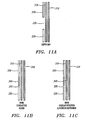
- the resistor chain 245 comprises three different types of gap designs: an empty gap; a gap with a conductive island 340; and a gap with an electrode extension of an overlap-resistor electrode 305 (e.g., a "T"). These three types are illustrated in Figs . 11a -c. Even if the gaps are all the same width, as illustrated in Figs. 11a -c, the three different gap designs provide different resistances between the resistor chain 245 and the touch region 206.
- the empty gap illustrated in Fig. 11a has the higher resistance, and a "T" shaped electrode extension 345 illustrated in Fig. 11c provides the lowest resistance.
- the empty gap will be wider and the "T" shaped electrode extension 345 will be narrower.
- This design degree of freedom to provide, in part, the desired parabolic resistance variations, has the beneficial result of reducing the needed variation in gap widths to some extent, thereby improving linearity. This flexibility also helps avoid tolerance issues involving the screen-printing of extremely small conductive islands 340 and gaps 335.
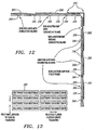
- the resistor chain 24 in addition to using conductive islands 340 within the junction gaps 335, also uses the different types of gap designs illustrated in Figs. 11a -c within the non-junction gaps 335 to provide the necessary parabolic resistance variation. Although it is generally desirable to use conductive islands 340 within the junction gaps 335 in order to improve ripple linearity along the non-sourcing side as previously discussed, it is sometimes desirable to use empty gap designs ( Fig. 11a ) for the junction gaps 335.
- the empty gap design in combination with a relatively narrow gap through which there is less of a problem of the touch region 206 "seeing" the unmixed voltages of the pair of electrodes 305 through the junction gap 335.
- Fig, 13 which illustrates an exemplary display of software touch buttons 355 that one may see when viewing the display of the touchscreen system 100.
- the touch buttons 355 are much wider than they are tall.
- the touchscreen system 100 must correctly determine the Y-coordinate with small errors, but only roughly determine the X-coordinate.
- the left and right sides of the electrode border are non-sourcing and the top and bottom sides are sourcing.
- Such a design leads to increased ripple non-linearity along the top and bottom for the X-coordinate measurement, but this is of secondary importance for applications, such as that illustrated in Fig. 13 .
- resistive touchscreen system 100 Although the above discussion has been set forth in the context of a resistive touchscreen system 100, it applies to the more general setting of a touch-sensitive system. This includes other types of touch sensors (e.g., opaque touch pads or touch sensitive robot shells). A variety of sensors with sensitive surfaces can be imagined. Indeed, the resistive touchscreen system 100 is really just a specific type of a touch sensitive system, where the gradient sheet 195 and cover sheet 210 are specifically designed to operate in the touchscreen 105. Thus, the present discussion, in its broadest aspects, should be thought of as applying in that more general setting.
- touch sensors e.g., opaque touch pads or touch sensitive robot shells.
- the resistive touchscreen system 100 is really just a specific type of a touch sensitive system, where the gradient sheet 195 and cover sheet 210 are specifically designed to operate in the touchscreen 105.
- the present discussion in its broadest aspects, should be thought of as applying in that more general setting.
Abstract
Description
- This application claims the benefit of the filing date of United States Provisional Patent Application Ser. No.
60/373,022, filed April 16, 2002 - The field of the present invention relates to touch sensor technology, and more particularly to resistive and capacitive touch sensor technology.
- Touch sensors are transparent or opaque input devices for computers and other electronic systems. As the name suggests, touch sensors are activated by touch, either from a user's finger, or a stylus or some other device. Transparent touch sensors, and specifically touchscreens, are generally placed over display devices, such as cathode ray tube (CRT) monitors and liquid crystal displays, to create touch display systems. These systems are increasingly used in commercial applications such as restaurant order entry systems, industrial process control applications, interactive museum exhibits, public information kiosks, pagers, cellular phones, personal digital assistants, and video games.
- The dominant touch technologies presently in use are resistive, capacitive, infrared, and acoustic technologies. Touchscreens incorporating these technologies have delivered high standards of performance at competitive prices. All are transparent devices that respond to a touch by transmitting the touch position coordinates to a host computer. An important aspect of touchscreen performance is a close correspondence between true and measured touch positions at all locations within a touch sensitive area located on the touch sensor (i.e., the touch region).
- One type of resistive touchscreen, and specifically a 5-wire resistive touchscreen, e.g., the AccuTouch™ product line of Elo TouchSystems, Inc. of Fremont, California, has been widely accepted for many touchscreen applications. In these touchscreens, mechanical pressure from a finger or stylus causes a plastic membrane coversheet to flex and make physical contact with an underlying glass substrate. The glass substrate is coated with a resistive layer upon which voltage gradients are excited via electrode patterns that are disposed along the periphery of the substrate. Via electrical connections to the four corners of the coated glass substrate, associated electronics can sequentially excite gradients in both the X and Y directions, as described in
U.S. Patent No. 3,591,718 . The underside of the coversheet has a conductive coating that provides electrical continuity between the touch location and voltage sensing electronics. Further details regarding 5-wire resistive touchscreens are found inU.S. Patent Nos. 4,220,815 ,4,661,655 ,4,731,508 ,4,822,957 ,5,045,644 , and5,220,136 .. - In a typical 5-wire resistive touchscreen, an electrode pattern along each border of the substrate is operated in both a "sourcing" mode and a "non-sourcing" mode. For example,
Figs. 1 and 2 illustrate atouch screen substrate 2 in which respective X and Y excitations are produced on atouch region 4 by applying different corner voltages (in this case, 5 volts) to anelectrode pattern 6 extending along theperiphery 8 of thesubstrate 2. The arrows represent the direction of current flow across thetouch region 4, and the dotted lines represent equipotential lines, i.e., lines along which the voltage is constant. For ideal linear touchscreen performance, the equipotential lines are perfectly straight lines, as suggested inFigs. 1 and 2 . Current flows perpendicular to these equipotential lines, so lines of current flow are straight when the equipotential lines are straight. - As shown in
Fig.1 , an X excitation is generated by passing current through thetouch region 4 injected at the right side of theborder electrode pattern 6 and collected at the left side. That is, the left and right sides are in "sourcing" (or sinking) mode for the X excitation. Ideally, for X excitation, no current enters or exits thetouch region 4 from the top and bottom sides. That is the top and bottom sides are "non-sourcing" for the X excitation. - As shown in
Fig. 2 , a Y excitation is generated by passing current through thetouch region 4 injected at the top side of theborder electrode pattern 6 and collected at the bottom side. That is, the top and bottom sides are in "sourcing" (or sinking) mode for the Y excitation. Ideally, for Y excitation, no current enters or exits thetouch region 4 from the left and right sides. That is, the left and right sides are "non-sourcing" for the Y excitation.Electronics can obtain touch information from a 5-wire resistive touchscreen via the voltage excitation described above, as well as current injection and capacitive architectures. A 9-wire connection scheme, which provides drive and a sense line connections between the electronics and each of the four corner connection points, is also available. These and other technologies are described inU.S. Patent Application Ser. No. 091705,383 - One 5-wire connection touch sensor utilizes peripheral electrode patterns with discrete overlap resistors, such as those found in Elo TouchSystems' AccuTouch™ products and disclosed in
U.S. Patent No. 5,045,644 . In this case, parallel resistive current paths are provided through gaps within isolation lines between peripheral electrode patterns on opposite sides of the touch region. The current paths produce an undesirable ripple non-linearity in the touch region near the peripheral electrode pattern. As a result, a finger moving across a straight line in this region will experience variations in the excitation voltage and hence variations in the measured coordinate (unless otherwise corrected for). The considerable ripple adjacent to the top and bottom resistor chains limits the accuracy of measurements in this area, and thus, the size of the effective touch region is therefore reduced. - As a result, resistor chains have been designed to reduce the ripple often found at the periphery of the touch region.
U.S. Patent Application Ser. No. 09/705,383 discloses an approach that reduces the ripple non-linearity on the sourcing sides of the touchscreen substrate by increasing the density of discrete electrical connections between the electrode border and the touch region, i.e., the number of gaps within the isolation lines are increased. - A problem arises in that while increasing the density of discrete electrical connections between the electrode border and the touch region improves linearity on the source sides, it provides more opportunities for parasitic sourcing and sinking of current on the non-sourcing sides. A higher density of electrical connections on the non-sourcing side tends to make matters worse. In particular, if there are more connections for the touch region than there are electrode voltages, then it is hard to avoid pairs of connections to the same electrode voltage and the consequent distortion of the desired linear voltage gradient. In practice, great linearity improvement on the sourcing sides is provided with a modest decrease in linearity on the non-sourcing sides. While this may appear to be quite a reasonable engineering trade-off, the marketplace is wary of anything that degrades any aspect of touchscreen performance.
- This problem was conceptually addressed in
U.S. Patent Application Ser. No. 09/705,383 by locating some of these gaps over the junctions between the electrodes, so that the effective voltage within these gaps is halfway between the voltages of adjacent electrodes. For example,Fig. 3 shows aresistor chain 48 having Z-electrodes 50 with overlapping outer andinner portions inner portions 52 of adjacent electrodes being closest atjunctions 54. An array ofinsulating regions 55 having twogaps 56 for eachoverlap resistor electrode 50 runs parallel to theinner portions 52. Some of thegaps 56 are over thejunctions 54. As shown in the equivalent circuit ofFig. 4 , this conceptually results in alternating connections being split between twoadjacent electrodes 50, so that the effective voltage is halfway between the voltages of theadjacent electrodes 50, thereby decreasing the ripple on the non-sourcing sides of the touchscreen. The main current through the series resistor chain in non-sourcing mode is notated by the "I", while a secondary current "i" flows through the junction gap region, which is conceptually equivalent to a simple resistive voltage divider circuit composed of two equal resistances. Thus, as can be seen, the gap voltage sequence is VN-1, (VN-1 + VN)/2, VN, (VN + VN+1)/2, VN+1 ... - It has been determined, however, that the effective voltage between
adjacent electrodes 50 does not divide in practice. Theinsulating regions 55 are typically placed very close to the seriesresistor chain electrodes 50 in response to marketplace demand for minimal border width. The result is a gap width that is typically much bigger than the separation from the seriesresistor chain electrodes 50. With such an aspect ratio, there is insufficient room for the electrode voltages VN and VN+1 to mix together and present an averaged voltage (VN + VN+1)/2 to the touchscreen. Effectively, the equipotential lines of the touch region "see" both electrode voltages. Hence, the VN and VN+1 equipotential lines tend to terminate on theelectrodes 50, and all the equipotential lines in between VN and VN+1 bunch up at thejunction 54, as illustrated inFig. 5 . As such, theresistor chain 48 ofFig. 3 will, in practice, have the equivalent circuit illustrated inFig. 6 . -
US patent 6163313 , on which the preamble ofclaim 1 is based, discloses a position touch sensor having a substrate and a resistive layer disposed on the substrate. At least one pair of electrodes is positioned on the resistive layer. A portion of one electrode is spaced from a portion of another electrode to produce an overlapped resistive region between the spaced portions of the electrodes. An insulating region extends into and terminates in the overlapped resistive region from a resistive region of the resistive layer outside the overlapped resistive region.
There remains a need to improve the non-sourcing side linearity of touchscreens with discrete resistor structures. - The present invention is directed to a touch sensor that utilizes electrically conductive islands in junction gaps in order to provide a true voltage divider within the gaps, thereby providing a linearly varying voltage sequence along the resistor chain. The touch sensor can be operated as a resistive touch sensor, e. g. , 5-or 9-wire, a capacitive touch sensor, or any touch sensor that requires series resistive chains.
In accordance with the present invention, there is provided a touch sensor as claimed in any of the accompanying claims.
By locating a conductive island within a junction gap, a voltage divider is formed within the junction gap, thereby minimizing bunching of equipotential lines on the electrodes during the non-sourcing mode. In the preferred embodiment, a conductive island is located within a plurality of the junction gaps to provide maximum benefit. To provide varying resistance between different gaps, e. g., a parabolic varying resistance along the length of the resistor chain, the non-junction gaps can be variously designed. For example, to provide maximum resistance, a non-junction gap may be empty, i. e. , it contains no electrically conductive material. To provide minimum resistance, the non-junction gap may contain an extension from the inner portion of the electrode. To provide a resistance somewhere in between, the non-junction gap may contain a conductive island. - The drawings illustrate the design and utility of a preferred embodiment of the present invention, in which similar elements are referred to by common reference numerals. In order to better appreciate the advantages and objects of the present invention, reference should be made to the accompanying drawings that illustrate this preferred embodiment. However, the drawings depict only one embodiment of the invention, and should not be taken as limiting its scope. With this caveat, the invention will be described and explained with additional specificity and detail through the use of the accompanying drawings in which:
-
Fig. 1 is a plan view of a prior art touchscreen being operated to provide X- excitation signals, so that the left and right sides are in the sourcing mode, and the top and bottom sides are in the non-sourcing mode; -
Fig. 2 is a plan view of a prior art touchscreen being operated to provide Y-excitation signals, so that the left and right sides are in the non-sourcing mode, and the top and bottom sides are in the sourcing mode; -
Fig. 3 is a schematic of a series resistor chain having two gaps (one junction and one non-junction) per overlap resistor electrode; -
Fig. 4 is an equivalent circuit for the resistor chain ofFig. 3 ; -
Fig. 5 is a schematic of a portion of the series resistor chain ofFig. 3 , particularly showing equipotential lines non-linearly terminating on the resistor chain when operated in the non-sourcing mode; -
Fig. 6 is a practical equivalent circuit for the resistor chain ofFig. 3 , particularly showing current flow and voltage potential; -
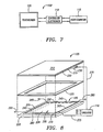
Fig. 7 is a functional diagram of a touch system constructed in accordance with a preferred embodiment of the present inventions; -
Fig. 8 is an exploded view of a touchscreen used in the touch system ofFig. 7 ; -
Fig. 9 is a schematic of a series resistor chain used in the touchscreen ofFig. 7 ; -
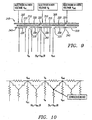
Fig. 10 is an equivalent circuit for resistor chain ofFig. 9 ; -
Figs. 11a -c are schematics of different types of gap arrangements that can be used in the series resistor chain ofFig. 9 ; -
Fig. 12 is a plan view of the top right corner of a gradient sheet used in the touchscreen ofFig. 7 ; and -
Fig.13 is a plan view of a display, particularly showing software touch buttons that require having asymmetric positional accuracy requirements in the X- and Y-directions. - Referring to
Fig. 7 , aresistive touchscreen system 100 constructed in accordance with a preferred embodiment of the present invention is described. Thetouchscreen system 100 generally comprises a touchscreen 105 (i.e., a touch sensor having a transparent substrate),controller electronics 110, and a display 120. Thetouchscreen system 100 is typically coupled to ahost computer 115. Generally, thecontroller electronics 110 receives from thetouchscreen 105 analog signals carrying touch information. Thecontroller electronics 110 also sends to thetouchscreen 105 excitation signals. Specifically, thecontroller electronics 110 establishes a voltage gradient across thetouchscreen 105. The voltages at the point of contact are representative of the position touched. Thecontroller electronics 110 digitizes these voltages and transmits these digitized signals, or touch information in digital form based on these digitized signals, to thehost computer 115 for processing. - Referring to
Fig. 8 , thetouchscreen 105 will now be described in further detail. It will be recognized that the thickness, height, or other dimensions of some of the components in some of the drawings has been exaggerated for purposes of illustration. Thetouchscreen 105 comprises agradient sheet 195 including asubstrate 200 having a uniformresistive layer 205 permanently applied to one surface thereof. Theresistive layer 205 further includes atouch region 206. - The geometry of the
substrate 200 may be, for example, planar (as shown inFig. 8 ), or may be contoured to match the face of a curved object, such as a Cathode Ray Tube (CRT) face or other conventional video display screens. Thesubstrate 200 can also have any perimeter configuration, e.g., rectangular (as shown), substantially rectangular, or circular. - To provide the necessary transparency, the
substrate 200 andresistive layer 205 are preferably made of a substantially transparent material. Alternatively, if the resultant product is to be an opaque sensor, then thesubstrate 200 may be composed of an opaque material. Spaced a small distance above theresistive layer 205 is acover sheet 210, which is typically aflexible film 215 having aconductive coating 220 on the underside of theflexible film 215. Thecover sheet 210 is joined to the remainder of thetouchscreen 105 with an adhesive along its associated edges, or optionally, with an insulativeadhesive frame 225 or the like. Additionally, anelectrode 230 connects theconductive coating 220 of thecover sheet 210 vialead 235 to appropriate external circuitry, such as thecontroller circuit 110. Theconductive coating 220 attached to thecover sheet 210 is separated from theresistive layer 205 by a plurality of small transparent insulator islands ordots 240, which prevent accidental contact between theconductive coating 220 and theresistive layer 205. - While the embodiment depicted in
Fig. 8 utilizes thecover sheet 210, any conducting element, such as a conducting stylus (not shown), can be used as an alternative. This conducting stylus may be used when theresistive layer 205 is sufficiently durable as to withstand damage from such contact. As another alternative, a capacitive or resistive pickup system can be used along with a user's finger or with an appropriate probe. - With continuing reference to
Fig. 8 , aresistor chain 245 is spaced along each edge of theresistive layer 205 and is used for applying potentials to theresistive layer 205, so as to create orthogonal voltage gradients therein. As to be shown in subsequent figures, the resistor chain 245 (composed of conductive regions, insulating regions, and resistive regions) includes discrete resistance units connected in series. The resistance values of theresistor chain 245 depend partly upon the resistive value of theresistive layer 205 that forms part of theresistor chain 245. However, the resistance values of theresistor chain 245 may vary in accordance with design requirements. There are fourresistor chains 245 in the embodiment ofFig. 8 , which are more specifically labeled 250, 255, 260, and 265. The ends of eachresistor chain corners 270 of theresistive layer 205. Each of thecorners 270 is provided with a respective one of theelectrical leads touchscreen 105 is connected to thecontroller electronics 110, which provides the voltage to theresistor chain 245 and processes information from thetouchscreen 105. - When the
touchscreen 105 is pressed, theconductive coating 220 of thecover sheet 210 makes direct electrical contact with theresistive layer 205 on thesubstrate 200. For a quasi-DC resistive touchscreen, commonly referred to as a "resistive touchscreen," thecover sheet 210 can function as either a voltage sensing probe for sensing the voltage at the contacted area, or as a current injection source. As another option, thecoversheet 210 may be replaced with a thin dielectric coating applied directly toresistive layer 205, in which case, thecontroller electronics 110 may support AC operation. - Further details on the general construction of
touch screen system 100 is disclosed inU.S. Patent Ser. No. 6,163,313 . - Referring now to
Fig. 9 , a portion of theresistor chain 245 will now be described in further detail. Theresistor chain 245 has Z-shapedelectrodes 305, each having anouter portion 310 and aninner portion 315. Theinner portion 315 of afirst electrode 305 overlaps theouter portion 310 of a second,adjacent electrode 305. As a result, the resistive layer 205 (shown inFig. 8 ) between these inner and outer portions forms aresistive connection 320. Theinner portions 315 ofadjacent electrodes 305 are separated from each other byjunctions 325. A plurality of insulatingregions 330 are formed in the gradient sheet 195 (shown inFig. 8 ), for example, by removing theresistive layer 205 at selected places. Thereafter, areas ofresistive coating 205 remain between adjacent insulatingregions 330, referred to herein as "gaps" 335. Some of thegaps 335 are positioned between theinner portions 315 of theelectrodes 305 and the touch region 206 (referred to as "non-junction gaps") and some of thegaps 335 are positioned between thejunctions 325 and the touch region 206 (referred to as "junction gaps"). - The insulating
regions 330 andgaps 335 may also be formed by removing a line of the resistive layer 205 (an insulation line) and thereafter placing resistive material, such as ITO, on the sheet at selected places along the insulation line. In the illustrated embodiment, the insulatingregions 330 andgaps 335 are formed in a line parallel to theinner portions 315 of theelectrodes 305. As a result, a plurality of parallel current paths across thetouch region 206 are established. The insulatingregions 330 may be readily formed by laser ablation of theresistive layer 205. Insulating subsections extending between theelectrodes 305 may also be formed. Laser adjustment of these subsections effectively trims the resistors between theelectrodes 305. - In order to achieve the object of a true voltage divider at the
junction 325 betweenadjacent electrodes 305, a conductive region or "island" 340 is positioned within thejunction gaps 335. The conductive material may be, e.g., a conductive frit. As a result, the VN equipotential line in thetouch region 206 no longer "sees" the electrode with voltage VN through thejunction gap 335, because theconductive island 340 cleanly provides the electronic node for the desired equivalent circuit, as illustrated inFig. 10 . - Simulations and prototype touchscreens have shown that the use of
conductive islands 340 within thejunction gaps 335 not only avoids increased ripple non-linearity on the non-sourcing side, but in fact, compared to existing commercial products with one electrical connection per overlap-resistor electrode, linearity on the non-sourcing side is improved. The reason for this improvement can be appreciated inFig. 9 , which illustrates equipotential lines of thetouch region 206 as they approach the electrode border. Because a conducting region is at a constant voltage, at most one equipotential line can terminate on aconductive electrode 305 or conductingisland 340. In contrast, many equipotential lines may terminate on ainsulating region 330. Loosely speaking, conducting regions connected to the touch region through thegaps 335 "repel" equipotential lines. The wider the gap is, the larger the distortion of the equipotential lines, and hence the greater is the ripple non-linearity. Replacing a large gap with a conductive island surrounded by two smaller gaps can provide a significant net gain in non-sourcing ripple non-linearity. - Thus, minimizing gap widths minimizes the amount of non-sourcing ripple non-linearity. It should be noted, however, that wider gaps are preferred for minimizing sourcing ripple non-linearity. As a result, it is best to avoid too much variation in gap widths. This desire to avoid unnecessary variation in gap widths, however, competes with another design requirement. As is well known in the prior art, a linear touchscreen design requires a parabolic variation in resistance of the connections between the touch region and the resistor chain series. As such, it is preferred that the gap widths, at least in the prior art, vary.
- Given this, the
resistor chain 245 preferably employs a variety of gap designs. Specifically, theresistor chain 245 comprises three different types of gap designs: an empty gap; a gap with aconductive island 340; and a gap with an electrode extension of an overlap-resistor electrode 305 (e.g., a "T"). These three types are illustrated inFigs. 11a -c. Even if the gaps are all the same width, as illustrated inFigs. 11a -c, the three different gap designs provide different resistances between theresistor chain 245 and thetouch region 206. The empty gap illustrated inFig. 11a has the higher resistance, and a "T" shapedelectrode extension 345 illustrated inFig. 11c provides the lowest resistance. Alternatively, for the same resistance to thetouch region 206, the empty gap will be wider and the "T" shapedelectrode extension 345 will be narrower. Using this design degree of freedom to provide, in part, the desired parabolic resistance variations, has the beneficial result of reducing the needed variation in gap widths to some extent, thereby improving linearity. This flexibility also helps avoid tolerance issues involving the screen-printing of extremely smallconductive islands 340 andgaps 335. - As illustrated in
Fig. 12 , theresistor chain 245, in addition to usingconductive islands 340 within thejunction gaps 335, also uses the different types of gap designs illustrated inFigs. 11a -c within thenon-junction gaps 335 to provide the necessary parabolic resistance variation. Although it is generally desirable to useconductive islands 340 within thejunction gaps 335 in order to improve ripple linearity along the non-sourcing side as previously discussed, it is sometimes desirable to use empty gap designs (Fig. 11a ) for thejunction gaps 335. For example, in cases where a high resistance is desired, such as at thegaps 335 adjacent the corners, it may be advantageous to use the empty gap design in combination with a relatively narrow gap through which there is less of a problem of thetouch region 206 "seeing" the unmixed voltages of the pair ofelectrodes 305 through thejunction gap 335. - It should be noted that in some applications, it may be desirable to fully optimize the linearity of one coordinate at the expense of increased border ripple non-linearity in the other coordinate, e.g., when there exists an application that has unequal demands for X and Y linearity. For example, consider
Fig, 13 , which illustrates an exemplary display ofsoftware touch buttons 355 that one may see when viewing the display of thetouchscreen system 100. As can be seen, thetouch buttons 355 are much wider than they are tall. Thus, for the user to correctly activate the intendedtouch button 355, thetouchscreen system 100 must correctly determine the Y-coordinate with small errors, but only roughly determine the X-coordinate. - As previously discussed, for Y-coordinate measurement, the left and right sides of the electrode border are non-sourcing and the top and bottom sides are sourcing. For such an application, it may be advantageous to use
gaps 335 withconductive islands 340 on the left and right sides of the electrode border, and then to use more than two gaps per electrode on the top and bottom sides of the electrode border. Such a design leads to increased ripple non-linearity along the top and bottom for the X-coordinate measurement, but this is of secondary importance for applications, such as that illustrated inFig. 13 . - Although the above discussion has been set forth in the context of a
resistive touchscreen system 100, it applies to the more general setting of a touch-sensitive system. This includes other types of touch sensors (e.g., opaque touch pads or touch sensitive robot shells). A variety of sensors with sensitive surfaces can be imagined. Indeed, theresistive touchscreen system 100 is really just a specific type of a touch sensitive system, where thegradient sheet 195 andcover sheet 210 are specifically designed to operate in thetouchscreen 105. Thus, the present discussion, in its broadest aspects, should be thought of as applying in that more general setting. - Although particular embodiments of the present invention have been shown and described, it should be understood that the above discussion is not intended to limit the present invention to these embodiments. Those of ordinary skill in the art will appreciate that various changes and modifications may be made without departing from then scope of the present invention. Thus, the present invention is intended to be defined by the claims.
Claims (16)
- A touch sensor (105), comprising:a substrate (200) having a resistive surface (205) bounded by a plurality of peripheral edges, said resistive surface having a touch region interior to said edges; andat least one series resistor chain (245) proximate one of said peripheral edges for creating electric fields across said touch region, the or each resistor chain comprising:characterised by at least one electrically conductive island (340) located within a junction gap.a plurality of resistors (320) formed from regions of said resistive surface as defined by a series of overlapping conductive electrodes (305) , wherein each electrode has an inner portion (315) facing said touch region, and wherein said inner portions of adjacent electrodes are separated by regions (325) of the resistive surface hereinafter referred to as junctions; anda linear array of insulating regions (330) in said resistive surface between said touch region and said resistor chain, said insulating regions being separated by gaps (335) wherein at least one of said gaps is formed adjacent a junction (325) hereinafter referred to as junction gap,
- The touch sensor (105) of claim 1, wherein junction gaps are formed adjacent at least a majority of said junctions (325).
- The touch sensor (105) of claim 1, wherein at least one gap is formed between adjacent junctions hereinafter referred to as a non-junction gap.
- The touch sensor (105) of claim 3, wherein non-junction gaps are formed between at least a majority of adjacent junctions (325).
- The touch sensor (105) of claim 3 further comprising at least one electrically conductive island (340) located within a non-junction gap.
- The touch sensor (105) of claim 3 further comprising at least one electrically conductive extension (345) from one of said inner portions (315) extending in to a non-junction gap.
- The touch sensor (105) of claim 1 wherein each of said electrodes (305) is a Z-shaped electrode.
- The touch sensor (105) of claim 1, wherein said substrate (200) is substantially transparent.
- The touch sensor (105) of claim 1, wherein said resistive surface (205) is fully intact within said gaps.
- The touch sensor (105) of claim 1, wherein said insulating regions (330) run parallel to said resistor chain.
- The touch sensor (105) of claim 1, wherein said array of insulating regions (330) is a line where said resistive surface (205) has been removed, said line being parallel to said resistor chain (245).
- The touch sensor (105) of claim 1, wherein the electric fields are non-linear.
- The touch sensor (105) of claim 1, further comprising a dielectric coating disposed over said touch region.
- A touch sensor (105) according to claim 1 wherein comprising two such series resistor chains (245) proximate opposing peripheral edges.
- The touch sensor (105) of claim 14, wherein said peripheral edges terminate at four corners.
- The touch sensor (105) of claim 14, wherein the linear array of insulating regions (330) of one resister chain (245) has two gaps (335) per resistor (320), and the linear array of insulating regions (330) of the other resister chain (245) has at least three gaps (335) per resistor (320).
Applications Claiming Priority (5)
| Application Number | Priority Date | Filing Date | Title |
|---|---|---|---|
| US37302202P | 2002-04-16 | 2002-04-16 | |
| US373022P | 2002-04-16 | ||
| PCT/US2003/011543 WO2003090156A2 (en) | 2002-04-16 | 2003-04-15 | Touch sensor with improved electrode pattern |
| US413825 | 2003-04-15 | ||
| US10/413,825 US20030231169A1 (en) | 2002-04-16 | 2003-04-15 | Touch sensor with improved electrode pattern |
Publications (2)
| Publication Number | Publication Date |
|---|---|
| EP1495440A2 EP1495440A2 (en) | 2005-01-12 |
| EP1495440B1 true EP1495440B1 (en) | 2010-01-20 |
Family
ID=29254506
Family Applications (1)
| Application Number | Title | Priority Date | Filing Date |
|---|---|---|---|
| EP03726288A Expired - Lifetime EP1495440B1 (en) | 2002-04-16 | 2003-04-15 | Touch sensor with improved electrode pattern |
Country Status (12)
| Country | Link |
|---|---|
| US (2) | US20030231169A1 (en) |
| EP (1) | EP1495440B1 (en) |
| JP (1) | JP4284196B2 (en) |
| KR (1) | KR100937288B1 (en) |
| CN (1) | CN100422919C (en) |
| AT (1) | ATE456107T1 (en) |
| AU (1) | AU2003228533A1 (en) |
| BR (1) | BR0309290A (en) |
| CA (1) | CA2482533A1 (en) |
| DE (1) | DE60331054D1 (en) |
| MX (1) | MXPA04010246A (en) |
| WO (1) | WO2003090156A2 (en) |
Families Citing this family (27)
| Publication number | Priority date | Publication date | Assignee | Title |
|---|---|---|---|---|
| US7307624B2 (en) * | 2003-12-30 | 2007-12-11 | 3M Innovative Properties Company | Touch sensor with linearized response |
| US7227538B2 (en) * | 2004-02-25 | 2007-06-05 | 3M Innovative Properties Company | Touch sensor with linearized response |
| DE102006059032B4 (en) * | 2006-12-14 | 2009-08-27 | Volkswagen Ag | Operating device of a motor vehicle and method for detecting user inputs |
| EP2118724A1 (en) * | 2007-02-02 | 2009-11-18 | Ampnt Inc. | Touch panel having closed loop electrode for equipotential build-up and manufacturing method thereof |
| JP5161594B2 (en) * | 2007-05-24 | 2013-03-13 | グンゼ株式会社 | Touch panel |
| GB2458464A (en) * | 2008-03-18 | 2009-09-23 | Young Fast Optoelectronics Co | Touch panel signal transfer assembly |
| FR2929022B1 (en) * | 2008-03-20 | 2011-08-26 | Young Fast Optoelectronics Co | SIGNAL TRANSFER ASSEMBLY FOR A TOUCH PANEL. |
| US20100309166A1 (en) * | 2008-04-10 | 2010-12-09 | Sharp Kabushiki Kaisha | Touch panel and display device equipped with the same |
| US7936111B2 (en) * | 2008-08-07 | 2011-05-03 | Samsung Electronics Co., Ltd. | Apparatus for generating electrical energy and method for manufacturing the same |
| TWI401588B (en) * | 2008-12-26 | 2013-07-11 | Higgstec Inc | Touch panel with parallel electrode pattern |
| TWI372351B (en) * | 2009-02-20 | 2012-09-11 | Higgstec Inc | Touch panel with non-continuous resistor chain |
| TWI497356B (en) * | 2009-02-20 | 2015-08-21 | Higgstec Inc | Touch panel with uniformed electrode pattern |
| KR101602372B1 (en) * | 2009-04-22 | 2016-03-11 | 삼성디스플레이 주식회사 | Touch panel nad noise elliminating method therefor |
| TWI390281B (en) | 2009-06-05 | 2013-03-21 | Higgstec Inc | Micro-matrix electrode and the touch panel thereof |
| WO2011152560A1 (en) * | 2010-06-04 | 2011-12-08 | Gunze Limited | Touch panel |
| JP5970776B2 (en) * | 2010-11-01 | 2016-08-17 | ぺんてる株式会社 | Coordinate input panel |
| KR101680256B1 (en) * | 2010-11-08 | 2016-12-13 | 삼성디스플레이 주식회사 | Touch Screen Panel in Resistive Type |
| JP5757800B2 (en) * | 2011-06-24 | 2015-08-05 | 富士通コンポーネント株式会社 | Touch panel |
| KR101885641B1 (en) * | 2011-09-22 | 2018-08-07 | 엘지디스플레이 주식회사 | Touch sensing apparatus and display device using the same |
| US9360971B2 (en) | 2012-02-10 | 2016-06-07 | 3M Innovative Properties Company | Mesh patterns for touch sensor electrodes |
| TWI571912B (en) * | 2012-05-04 | 2017-02-21 | 群康科技(深圳)有限公司 | Method for making narrow electric wires on the peripheral region of touch screen, the touch screen containing the said wires, and display screen apparatus |
| CN103384451A (en) * | 2012-05-04 | 2013-11-06 | 群康科技(深圳)有限公司 | Manufacturing method for touch panel edge wire routing, touch panel and touch display device |
| CN103793089B (en) * | 2012-10-30 | 2017-05-17 | 宸鸿科技(厦门)有限公司 | Touch panel |
| US9280240B2 (en) * | 2012-11-14 | 2016-03-08 | Synaptics Incorporated | System and method for finite element imaging sensor devices |
| CN104063110B (en) | 2013-03-21 | 2017-12-15 | 奇畿科技股份有限公司 | The electrode loop structure of contact panel |
| TWI710947B (en) * | 2015-11-02 | 2020-11-21 | 奇畿科技股份有限公司 | Linear adjustment and compensation method and structure for resistive touch panel |
| US11237687B2 (en) | 2019-01-25 | 2022-02-01 | Samsung Electronics Co., Ltd. | Systems and methods for touch detection using electric field tomography through resistive sheet |
Family Cites Families (11)
| Publication number | Priority date | Publication date | Assignee | Title |
|---|---|---|---|---|
| US4371746A (en) * | 1978-01-05 | 1983-02-01 | Peptek, Incorporated | Edge terminations for impedance planes |
| US4220815B1 (en) * | 1978-12-04 | 1996-09-03 | Elographics Inc | Nonplanar transparent electrographic sensor |
| US4622437A (en) * | 1984-11-29 | 1986-11-11 | Interaction Systems, Inc. | Method and apparatus for improved electronic touch mapping |
| US4822957B1 (en) * | 1984-12-24 | 1996-11-19 | Elographics Inc | Electrographic touch sensor having reduced bow of equipotential field lines therein |
| US4661655B1 (en) * | 1984-12-24 | 1997-01-21 | Elographics Inc | Electrographic touch sensor and method of reducing bowed equipotential fields therein |
| WO1987004553A1 (en) * | 1986-01-17 | 1987-07-30 | Interaction Systems, Inc. | Method and apparatus for improved electronic touch mapping |
| US5045644A (en) * | 1990-04-16 | 1991-09-03 | Elographics, Inc. | Touch sensitive screen with improved corner response |
| US5220136A (en) * | 1991-11-26 | 1993-06-15 | Elographics, Inc. | Contact touchscreen with an improved insulated spacer arrangement |
| US6163313A (en) * | 1997-12-12 | 2000-12-19 | Aroyan; James L. | Touch sensitive screen and method |
| US6549193B1 (en) * | 1998-10-09 | 2003-04-15 | 3M Innovative Properties Company | Touch panel with improved linear response and minimal border width electrode pattern |
| US6593916B1 (en) * | 2000-11-03 | 2003-07-15 | James L. Aroyan | Touchscreen having multiple parallel connections to each electrode in a series resistor chain on the periphery of the touch area |
-
2003
- 2003-04-15 CN CNB038134640A patent/CN100422919C/en not_active Expired - Fee Related
- 2003-04-15 AT AT03726288T patent/ATE456107T1/en not_active IP Right Cessation
- 2003-04-15 US US10/413,825 patent/US20030231169A1/en not_active Abandoned
- 2003-04-15 AU AU2003228533A patent/AU2003228533A1/en not_active Abandoned
- 2003-04-15 BR BR0309290-9A patent/BR0309290A/en not_active IP Right Cessation
- 2003-04-15 EP EP03726288A patent/EP1495440B1/en not_active Expired - Lifetime
- 2003-04-15 WO PCT/US2003/011543 patent/WO2003090156A2/en active Application Filing
- 2003-04-15 MX MXPA04010246A patent/MXPA04010246A/en unknown
- 2003-04-15 CA CA002482533A patent/CA2482533A1/en not_active Abandoned
- 2003-04-15 KR KR1020047016605A patent/KR100937288B1/en not_active IP Right Cessation
- 2003-04-15 JP JP2003586826A patent/JP4284196B2/en not_active Expired - Lifetime
- 2003-04-15 DE DE60331054T patent/DE60331054D1/en not_active Expired - Lifetime
-
2005
- 2005-11-03 US US11/267,759 patent/US7952567B2/en active Active
Also Published As
| Publication number | Publication date |
|---|---|
| WO2003090156A3 (en) | 2004-02-12 |
| CN1659582A (en) | 2005-08-24 |
| US20030231169A1 (en) | 2003-12-18 |
| JP2005523531A (en) | 2005-08-04 |
| WO2003090156A9 (en) | 2004-03-25 |
| JP4284196B2 (en) | 2009-06-24 |
| US20060119587A1 (en) | 2006-06-08 |
| WO2003090156A2 (en) | 2003-10-30 |
| CN100422919C (en) | 2008-10-01 |
| AU2003228533A1 (en) | 2003-11-03 |
| CA2482533A1 (en) | 2003-10-30 |
| BR0309290A (en) | 2005-02-01 |
| US7952567B2 (en) | 2011-05-31 |
| MXPA04010246A (en) | 2005-07-05 |
| ATE456107T1 (en) | 2010-02-15 |
| DE60331054D1 (en) | 2010-03-11 |
| KR20040101511A (en) | 2004-12-02 |
| KR100937288B1 (en) | 2010-01-18 |
| EP1495440A2 (en) | 2005-01-12 |
Similar Documents
| Publication | Publication Date | Title |
|---|---|---|
| US7952567B2 (en) | Touch sensor with improved electrode pattern | |
| US6163313A (en) | Touch sensitive screen and method | |
| CA2396763C (en) | Touchscreen having multiple parallel connections to each electrode in a series resistor chain on the periphery of the touch area | |
| US8054738B2 (en) | Touch panel, method for driving same, and display device using the same | |
| TWI424337B (en) | Two-dimensional position sensor | |
| US8698769B2 (en) | Dual mode capacitive touch panel | |
| US6690361B1 (en) | Touch panel | |
| AU2004260408A1 (en) | Touch sensor with non-uniform resistive band | |
| JP2009009291A (en) | Screen input type image display device | |
| JPH0638223B2 (en) | Graph touch sensor | |
| US20090079708A1 (en) | Three-wire resistive touch panel and display device using same | |
| US7180505B2 (en) | Touch panel for display device | |
| KR100369903B1 (en) | Touch panel input device | |
| TWI302668B (en) | Touch sensor with improved electrode pattern | |
| AU785406B2 (en) | Touchscreen having multiple parallel connections to each electrode in a series resistor chain on the periphery of the touch area | |
| JP2001273084A (en) | Coordinate input device |
Legal Events
| Date | Code | Title | Description |
|---|---|---|---|
| PUAI | Public reference made under article 153(3) epc to a published international application that has entered the european phase |
Free format text: ORIGINAL CODE: 0009012 |
|
| 17P | Request for examination filed |
Effective date: 20041102 |
|
| AK | Designated contracting states |
Kind code of ref document: A2 Designated state(s): AT BE BG CH CY CZ DE DK EE ES FI FR GB GR HU IE IT LI LU MC NL PT RO SE SI SK TR |
|
| AX | Request for extension of the european patent |
Extension state: AL LT LV MK |
|
| 17Q | First examination report despatched |
Effective date: 20071218 |
|
| 18D | Application deemed to be withdrawn |
Effective date: 20080701 |
|
| 18RA | Request filed for re-establishment of rights before grant |
Effective date: 20090402 |
|
| 18RR | Decision to grant the request for re-establishment of rights before grant |
Free format text: ANGENOMMEN Effective date: 20090701 |
|
| GRAP | Despatch of communication of intention to grant a patent |
Free format text: ORIGINAL CODE: EPIDOSNIGR1 |
|
| RIC1 | Information provided on ipc code assigned before grant |
Ipc: G06F 3/045 20060101ALI20090811BHEP Ipc: G06K 11/06 20060101AFI20090811BHEP |
|
| D18D | Application deemed to be withdrawn (deleted) | ||
| GRAS | Grant fee paid |
Free format text: ORIGINAL CODE: EPIDOSNIGR3 |
|
| GRAA | (expected) grant |
Free format text: ORIGINAL CODE: 0009210 |
|
| AK | Designated contracting states |
Kind code of ref document: B1 Designated state(s): AT BE BG CH CY CZ DE DK EE ES FI FR GB GR HU IE IT LI LU MC NL PT RO SE SI SK TR |
|
| REG | Reference to a national code |
Ref country code: CH Ref legal event code: EP |
|
| REG | Reference to a national code |
Ref country code: IE Ref legal event code: FG4D |
|
| REF | Corresponds to: |
Ref document number: 60331054 Country of ref document: DE Date of ref document: 20100311 Kind code of ref document: P |
|
| REG | Reference to a national code |
Ref country code: NL Ref legal event code: VDEP Effective date: 20100120 |
|
| PG25 | Lapsed in a contracting state [announced via postgrant information from national office to epo] |
Ref country code: AT Free format text: LAPSE BECAUSE OF FAILURE TO SUBMIT A TRANSLATION OF THE DESCRIPTION OR TO PAY THE FEE WITHIN THE PRESCRIBED TIME-LIMIT Effective date: 20100120 |
|
| PG25 | Lapsed in a contracting state [announced via postgrant information from national office to epo] |
Ref country code: ES Free format text: LAPSE BECAUSE OF FAILURE TO SUBMIT A TRANSLATION OF THE DESCRIPTION OR TO PAY THE FEE WITHIN THE PRESCRIBED TIME-LIMIT Effective date: 20100501 Ref country code: PT Free format text: LAPSE BECAUSE OF FAILURE TO SUBMIT A TRANSLATION OF THE DESCRIPTION OR TO PAY THE FEE WITHIN THE PRESCRIBED TIME-LIMIT Effective date: 20100520 Ref country code: NL Free format text: LAPSE BECAUSE OF FAILURE TO SUBMIT A TRANSLATION OF THE DESCRIPTION OR TO PAY THE FEE WITHIN THE PRESCRIBED TIME-LIMIT Effective date: 20100120 |
|
| PG25 | Lapsed in a contracting state [announced via postgrant information from national office to epo] |
Ref country code: SI Free format text: LAPSE BECAUSE OF FAILURE TO SUBMIT A TRANSLATION OF THE DESCRIPTION OR TO PAY THE FEE WITHIN THE PRESCRIBED TIME-LIMIT Effective date: 20100120 Ref country code: FI Free format text: LAPSE BECAUSE OF FAILURE TO SUBMIT A TRANSLATION OF THE DESCRIPTION OR TO PAY THE FEE WITHIN THE PRESCRIBED TIME-LIMIT Effective date: 20100120 |
|
| PG25 | Lapsed in a contracting state [announced via postgrant information from national office to epo] |
Ref country code: SE Free format text: LAPSE BECAUSE OF FAILURE TO SUBMIT A TRANSLATION OF THE DESCRIPTION OR TO PAY THE FEE WITHIN THE PRESCRIBED TIME-LIMIT Effective date: 20100120 Ref country code: EE Free format text: LAPSE BECAUSE OF FAILURE TO SUBMIT A TRANSLATION OF THE DESCRIPTION OR TO PAY THE FEE WITHIN THE PRESCRIBED TIME-LIMIT Effective date: 20100120 Ref country code: RO Free format text: LAPSE BECAUSE OF FAILURE TO SUBMIT A TRANSLATION OF THE DESCRIPTION OR TO PAY THE FEE WITHIN THE PRESCRIBED TIME-LIMIT Effective date: 20100120 Ref country code: BE Free format text: LAPSE BECAUSE OF FAILURE TO SUBMIT A TRANSLATION OF THE DESCRIPTION OR TO PAY THE FEE WITHIN THE PRESCRIBED TIME-LIMIT Effective date: 20100120 Ref country code: GR Free format text: LAPSE BECAUSE OF FAILURE TO SUBMIT A TRANSLATION OF THE DESCRIPTION OR TO PAY THE FEE WITHIN THE PRESCRIBED TIME-LIMIT Effective date: 20100421 Ref country code: CY Free format text: LAPSE BECAUSE OF FAILURE TO SUBMIT A TRANSLATION OF THE DESCRIPTION OR TO PAY THE FEE WITHIN THE PRESCRIBED TIME-LIMIT Effective date: 20100120 |
|
| PLBE | No opposition filed within time limit |
Free format text: ORIGINAL CODE: 0009261 |
|
| STAA | Information on the status of an ep patent application or granted ep patent |
Free format text: STATUS: NO OPPOSITION FILED WITHIN TIME LIMIT |
|
| PG25 | Lapsed in a contracting state [announced via postgrant information from national office to epo] |
Ref country code: SK Free format text: LAPSE BECAUSE OF FAILURE TO SUBMIT A TRANSLATION OF THE DESCRIPTION OR TO PAY THE FEE WITHIN THE PRESCRIBED TIME-LIMIT Effective date: 20100120 Ref country code: MC Free format text: LAPSE BECAUSE OF NON-PAYMENT OF DUE FEES Effective date: 20100430 Ref country code: CZ Free format text: LAPSE BECAUSE OF FAILURE TO SUBMIT A TRANSLATION OF THE DESCRIPTION OR TO PAY THE FEE WITHIN THE PRESCRIBED TIME-LIMIT Effective date: 20100120 Ref country code: BG Free format text: LAPSE BECAUSE OF FAILURE TO SUBMIT A TRANSLATION OF THE DESCRIPTION OR TO PAY THE FEE WITHIN THE PRESCRIBED TIME-LIMIT Effective date: 20100420 |
|
| REG | Reference to a national code |
Ref country code: CH Ref legal event code: PL |
|
| 26N | No opposition filed |
Effective date: 20101021 |
|
| PG25 | Lapsed in a contracting state [announced via postgrant information from national office to epo] |
Ref country code: DK Free format text: LAPSE BECAUSE OF FAILURE TO SUBMIT A TRANSLATION OF THE DESCRIPTION OR TO PAY THE FEE WITHIN THE PRESCRIBED TIME-LIMIT Effective date: 20100120 Ref country code: IE Free format text: LAPSE BECAUSE OF NON-PAYMENT OF DUE FEES Effective date: 20100415 |
|
| PG25 | Lapsed in a contracting state [announced via postgrant information from national office to epo] |
Ref country code: CH Free format text: LAPSE BECAUSE OF NON-PAYMENT OF DUE FEES Effective date: 20100430 Ref country code: LI Free format text: LAPSE BECAUSE OF NON-PAYMENT OF DUE FEES Effective date: 20100430 |
|
| PG25 | Lapsed in a contracting state [announced via postgrant information from national office to epo] |
Ref country code: IT Free format text: LAPSE BECAUSE OF FAILURE TO SUBMIT A TRANSLATION OF THE DESCRIPTION OR TO PAY THE FEE WITHIN THE PRESCRIBED TIME-LIMIT Effective date: 20100120 |
|
| PG25 | Lapsed in a contracting state [announced via postgrant information from national office to epo] |
Ref country code: HU Free format text: LAPSE BECAUSE OF FAILURE TO SUBMIT A TRANSLATION OF THE DESCRIPTION OR TO PAY THE FEE WITHIN THE PRESCRIBED TIME-LIMIT Effective date: 20100721 Ref country code: LU Free format text: LAPSE BECAUSE OF NON-PAYMENT OF DUE FEES Effective date: 20100415 |
|
| REG | Reference to a national code |
Ref country code: GB Ref legal event code: 732E Free format text: REGISTERED BETWEEN 20120906 AND 20120912 |
|
| REG | Reference to a national code |
Ref country code: DE Ref legal event code: R082 Ref document number: 60331054 Country of ref document: DE Representative=s name: MARKS & CLERK (LUXEMBOURG) LLP, LU |
|
| PG25 | Lapsed in a contracting state [announced via postgrant information from national office to epo] |
Ref country code: TR Free format text: LAPSE BECAUSE OF FAILURE TO SUBMIT A TRANSLATION OF THE DESCRIPTION OR TO PAY THE FEE WITHIN THE PRESCRIBED TIME-LIMIT Effective date: 20100120 |
|
| REG | Reference to a national code |
Ref country code: DE Ref legal event code: R082 Ref document number: 60331054 Country of ref document: DE Representative=s name: MARKS & CLERK (LUXEMBOURG) LLP, LU Effective date: 20121024 Ref country code: DE Ref legal event code: R081 Ref document number: 60331054 Country of ref document: DE Owner name: ELO TOUCH SOLUTIONS, INC., US Free format text: FORMER OWNER: TYCO ELECTRONICS CORP., BERWYN, US Effective date: 20121024 Ref country code: DE Ref legal event code: R081 Ref document number: 60331054 Country of ref document: DE Owner name: ELO TOUCH SOLUTIONS, INC., MENLO PARK, US Free format text: FORMER OWNER: TYCO ELECTRONICS CORP., BERWYN, PA., US Effective date: 20121024 |
|
| REG | Reference to a national code |
Ref country code: FR Ref legal event code: TP Owner name: ELO TOUCH SOLUTIONS, INC., US Effective date: 20130321 |
|
| REG | Reference to a national code |
Ref country code: FR Ref legal event code: PLFP Year of fee payment: 13 |
|
| PGFP | Annual fee paid to national office [announced via postgrant information from national office to epo] |
Ref country code: FR Payment date: 20150408 Year of fee payment: 13 |
|
| REG | Reference to a national code |
Ref country code: FR Ref legal event code: ST Effective date: 20161230 |
|
| PG25 | Lapsed in a contracting state [announced via postgrant information from national office to epo] |
Ref country code: FR Free format text: LAPSE BECAUSE OF NON-PAYMENT OF DUE FEES Effective date: 20160502 |
|
| PGFP | Annual fee paid to national office [announced via postgrant information from national office to epo] |
Ref country code: DE Payment date: 20200422 Year of fee payment: 18 |
|
| PGFP | Annual fee paid to national office [announced via postgrant information from national office to epo] |
Ref country code: GB Payment date: 20200422 Year of fee payment: 18 |
|
| REG | Reference to a national code |
Ref country code: DE Ref legal event code: R119 Ref document number: 60331054 Country of ref document: DE |
|
| GBPC | Gb: european patent ceased through non-payment of renewal fee |
Effective date: 20210415 |
|
| PG25 | Lapsed in a contracting state [announced via postgrant information from national office to epo] |
Ref country code: DE Free format text: LAPSE BECAUSE OF NON-PAYMENT OF DUE FEES Effective date: 20211103 Ref country code: GB Free format text: LAPSE BECAUSE OF NON-PAYMENT OF DUE FEES Effective date: 20210415 |