EP1494297A2 - Organic electroluminescent display - Google Patents
Organic electroluminescent display Download PDFInfo
- Publication number
- EP1494297A2 EP1494297A2 EP04015274A EP04015274A EP1494297A2 EP 1494297 A2 EP1494297 A2 EP 1494297A2 EP 04015274 A EP04015274 A EP 04015274A EP 04015274 A EP04015274 A EP 04015274A EP 1494297 A2 EP1494297 A2 EP 1494297A2
- Authority
- EP
- European Patent Office
- Prior art keywords
- organic
- display
- film
- grating pattern
- light
- Prior art date
- Legal status (The legal status is an assumption and is not a legal conclusion. Google has not performed a legal analysis and makes no representation as to the accuracy of the status listed.)
- Withdrawn
Links
Images


Classifications
-
- H—ELECTRICITY
- H05—ELECTRIC TECHNIQUES NOT OTHERWISE PROVIDED FOR
- H05B—ELECTRIC HEATING; ELECTRIC LIGHT SOURCES NOT OTHERWISE PROVIDED FOR; CIRCUIT ARRANGEMENTS FOR ELECTRIC LIGHT SOURCES, IN GENERAL
- H05B33/00—Electroluminescent light sources
- H05B33/12—Light sources with substantially two-dimensional [2D] radiating surfaces
- H05B33/22—Light sources with substantially two-dimensional [2D] radiating surfaces characterised by the chemical or physical composition or the arrangement of auxiliary dielectric or reflective layers
-
- H—ELECTRICITY
- H10—SEMICONDUCTOR DEVICES; ELECTRIC SOLID-STATE DEVICES NOT OTHERWISE PROVIDED FOR
- H10K—ORGANIC ELECTRIC SOLID-STATE DEVICES
- H10K59/00—Integrated devices, or assemblies of multiple devices, comprising at least one organic light-emitting element covered by group H10K50/00
- H10K59/80—Constructional details
- H10K59/875—Arrangements for extracting light from the devices
- H10K59/879—Arrangements for extracting light from the devices comprising refractive means, e.g. lenses
-
- H—ELECTRICITY
- H10—SEMICONDUCTOR DEVICES; ELECTRIC SOLID-STATE DEVICES NOT OTHERWISE PROVIDED FOR
- H10K—ORGANIC ELECTRIC SOLID-STATE DEVICES
- H10K50/00—Organic light-emitting devices
- H10K50/80—Constructional details
- H10K50/85—Arrangements for extracting light from the devices
- H10K50/858—Arrangements for extracting light from the devices comprising refractive means, e.g. lenses
Definitions
- the present invention relates to an organic electroluminescent display.
- the EL display is provided to a small mobile apparatus such as a mobile phone and is in common use.
- the organic EL display employed to the mobile apparatus requires long life span and low electric consumption. However, the organic EL display currently used is not satisfied with the condition.
- total inner reflection of a glass substrate and a loss of light from doparo effect reach about 80%. Therefore, brightness of the display is increased with a little electric consumption if the loss of light is reduced.
- a method of roughening a surface of the substrate, a method of forming a pattern with projections on the surface of the substrate, and a method of using semicircular lens in a millimeter size are employed as a method for reducing a light loss resulted from the inner reflection and doparo effect, and increasing the light efficiency.
- the methods have problems that a pattern of light radiation is changed, a displayed image is blurred, and manufacturing is difficult.
- the present invention is directed to an EL (electroluminescent) display that substantially obviates one or more problems due to limitations and disadvantages of the related art.
- An object of the present invention is to provide an EL display having an improved light emitting efficiency and displaying a clear image.
- an EL display includes a first electrode formed on the transparent substrate, an organic light emitting payer formed on the first electrode, a second electrode formed on the organic light emitting layer, and a film formed at a bottom of the transparent substrate and having a two-dimensional pattern on a surface thereof.
- the cycle of the two-dimensional grating pattern is less than 200nm and includes a plurality of projections.
- Each of the plurality of projections may be hexahedral and is arrayed in a matrix form at a same interval.
- the film is a macromolecular material being capable of intensifying heat or ultraviolet rays and having 85% of transmissivity.
- FIG. 1 illustrates a diagram showing a film having a two-dimensional grating pattern attached to an organic EL display in accordance with the present invention.
- FIG. 2 illustrates a diagram showing an organic EL display in accordance with the present invention.
- FIGs. 3A to 3E illustrate a diagram showing a manufacturing process of a mold for manufacturing a film of FIG. 1.
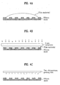
- FIGS. 4A to 4C illustrate a diagram showing a film manufacturing process of FIG. 1.
- the purpose of the present invention is manufacturing an organic EL (electroluminescent) display by using a film with a two-dimensional grating pattern for increasing luminescent efficiency of the display.
- FIG. 1 illustrates a diagram showing the film having a two-dimensional grating pattern attached to the organic EL display in accordance with the present invention.
- the two-dimensional grating pattern is formed on a surface of the film employed by the present invention.
- the two-dimensional grating pattern is that materials having a different refractive index are arrayed at a predetermined interval in two dimensions. In this case, one interval of the grating pattern is in a smaller size than a half wavelength of light. When a wavelength of a blue color is about 400nm, one interval of the grating pattern is about 200nm.
- the two-dimensional grating pattern with a smaller interval than the half wavelength of light does not diffract but penetrate light in 0-dimensional mode.
- An effective refractive index is lowered decreasing reflection of light so as to increase a luminous efficiency of the display.
- the two-dimensional grating pattern includes a plurality of projections. It is desirable that each of the plurality of projections is formed in a hexahedral form.
- the projection can be polyhedral, globular, and circular form.
- the projections are arrayed in a matrix form at a same interval.
- a material such as a macromolecule being capable of intensifying heat or ultraviolet rays and having 85% of transmissivity for manufacturing the film with the two-dimensional grating pattern.
- FIG. 2 illustrates a diagram showing the organic EL display in accordance with the present invention, and a manufacturing process of the organic EL display is as follows.
- a first electrode 2 is formed on a transparent substrate 1.
- the first electrode 2 being an anode employs ITO (indium tin oxide).
- the organic light-emitting layer 3 is formed on the first electrode 2.
- the organic light-emitting layer includes a HIL (hole injecting layer), a light emitting layer, an ETL (electron transport layer), and an EIL (electron injecting layer).
- HIL hole injecting layer
- ETL electron transport layer
- EIL electron injecting layer
- the HIL is formed in a size of 10-30nm.
- the HTL includes about 30-60nm of N,N'-diphenyl-N, N'-bis(3-methylphenyl)-(1-1'-biphenyl)-4, 4'-diamine(TPD) or, 4, 4'-bis[N-(1-naphthyl)-N-phenyl-amino]bipheny(NPD).
- Dopant is added to the light-emitting layer at need.
- the EIL includes a thin layer of about 5 ⁇ of LiF or Li 2 O, or under about 200 ⁇ of alkali metal or alkalito metal such as Li, Ca, Mg, and Sr.
- a second electrode 4 is formed on the organic light emitting layer 3 formed as abovementioned.
- the second electrode 4 being a cathode employs a high conductive metal.
- Total reflection of light is determined by an angle of light entering into the glass substrate 1, and again by refractive index of the glass 1.
- Amount of total reflection is increased by a large index of refraction. Therefore, if a film of smaller material than the refractive index of the glass on the glass substrate 1 is attached to, the amount of total reflection of light is decreased.
- a reflective index of the film 5 with the grating pattern becomes smaller than the film with no grating film such that a total reflection amount of light is further decreased.
- FIGS. 3A to 3E illustrate a diagram showing a manufacturing process of a mold for manufacturing a film of FIG. 1.
- a nitrifying silicon film 52 is formed on a silicon substrate 51 in a PECVD method.
- a sensitive emulsion 53 is formed on the nitrifying silicon film 52.
- the sensitive emulsion 53 needs to suit the process of work when an electron beam lithography or x-ray lithography is employed.
- the two-dimensional grating pattern is formed by a method of radiating or developing a light or electron beam to the sensitive emulsion 53 as illustrated in FIG. 3C.
- a mask is employed for forming the grating pattern.
- the grating pattern is directly formed without using any mask when the electron beam lithography is employed.
- an interfering pattern employed for forming the grating pattern the interfering pattern formed in a process of recombining separated laser lights.
- the nitrifying silicon film 52 is etched using the sensitive emulsion 53 as a mask as illustrated in FIG. 3D.
- a part of the silicon substrate 51 is removed by using the nitrifying silicon film 53 as the mask, and the silicon mold is completed removing the rest of nitrifying silicon film 53.
- the mold is manufactured using not only the silicon but also other materials such as Quartz.
- the mold may be manufactured by metal.
- a famous electroforming is employed.
- FIGS. 4A to 4C illustrates a diagram showing a film manufacturing process of FIG. 1.
- a film material 54 is injected onto the silicon mold illustrated in FIG. 3E.
- the film material is a macromolecule enabling intensifying heat or ultraviolet rays and has 85% of transmissivity.
- the macromolecular material is placed on top of the film material, pressed by using a hard plate such as the glass substrate, and attached to the silicon mold by heating or radiating.
- the thickness of the film is determined by pressure and a hardening condition.
- the plate for pressing needs to be parallel to the mold.
- the film needs to have high transmissivity.
- the film having the two-dimensional grating pattern is completed when the film is separated from the silicon mold.
- the film manufactured as abovementioned is attached to a bottom of the glass substrate.
- the grating pattern formed on the film is a reverse pattern of the pattern formed at the silicon mold.
- the present invention manufactures the film having the two-dimensional grating pattern using the silicon mold and has effects of increasing the light emitting efficiency of the organic EL display and displaying clear image.
Landscapes
- Physics & Mathematics (AREA)
- Optics & Photonics (AREA)
- Electroluminescent Light Sources (AREA)
- Devices For Indicating Variable Information By Combining Individual Elements (AREA)
- Diffracting Gratings Or Hologram Optical Elements (AREA)
Abstract
Description
In this case, a famous electroforming is employed.
Claims (10)
- An organic EL (electroluminescent) display, comprising: a transparent substrate,
an organic light-emitting layer formed on top of a first electrode;
a second electrode formed on the organic light-emitting layer;
a film formed at a bottom of the transparent substrate and having a two-dimensional grating pattern on a surface thereof. - The organic EL display of claim 1, wherein the cycle of the two-dimensional grating pattern is less than 200nm.
- The organic EL display of claim 1, wherein the two-dimensional grating pattern comprises a plurality of projections.
- The organic EL display of claim 3, wherein each of the plurality of projections is formed in one of polyhedral, semi-global, and circular forms.
- The organic EL display of claim 3, wherein each of the plurality of projections is arrayed in a matrix form.
- The organic EL display of claim 3, wherein each of the plurality of projections is arrayed at a same interval.
- The organic EL display of claim 1, wherein the film is macromolecule enabling intensifying heat or ultraviolet rays and having more than 85% of light transmissivity.
- The organic EL display of claim 1, wherein the film is manufactured by a mold having a reverse pattern of the two-dimensional grating pattern.
- The organic EL display of claim 8, wherein the mold is manufactured by using a semiconductor process, or an electroplating.
- The organic EL display of claim 8, wherein the mold comprises one of silicon, Quartz, GaAs, Ge, and nickel.
Applications Claiming Priority (2)
| Application Number | Priority Date | Filing Date | Title |
|---|---|---|---|
| KR1020030043639A KR100546652B1 (en) | 2003-06-30 | 2003-06-30 | Organic EL element |
| KR2003043639 | 2003-06-30 |
Publications (2)
| Publication Number | Publication Date |
|---|---|
| EP1494297A2 true EP1494297A2 (en) | 2005-01-05 |
| EP1494297A3 EP1494297A3 (en) | 2006-04-26 |
Family
ID=33432444
Family Applications (1)
| Application Number | Title | Priority Date | Filing Date |
|---|---|---|---|
| EP04015274A Withdrawn EP1494297A3 (en) | 2003-06-30 | 2004-06-29 | Organic electroluminescent display |
Country Status (5)
| Country | Link |
|---|---|
| US (1) | US7211945B2 (en) |
| EP (1) | EP1494297A3 (en) |
| JP (1) | JP4853605B2 (en) |
| KR (1) | KR100546652B1 (en) |
| CN (1) | CN1578566A (en) |
Cited By (1)
| Publication number | Priority date | Publication date | Assignee | Title |
|---|---|---|---|---|
| WO2007127513A3 (en) * | 2006-01-31 | 2008-04-17 | Dow Corning | Soft lithographic molding of surface relief output couplers for organic light emitting diodes |
Families Citing this family (6)
| Publication number | Priority date | Publication date | Assignee | Title |
|---|---|---|---|---|
| US20060083148A1 (en) * | 2004-10-18 | 2006-04-20 | Konica Minolta Holdings, Inc. | Planar light emitting device |
| JP5109318B2 (en) * | 2006-09-27 | 2012-12-26 | 凸版印刷株式会社 | Method for producing organic EL display using optical transfer sheet |
| US8110827B2 (en) * | 2007-04-04 | 2012-02-07 | Koninklijke Philips Electronics N.V. | Light emitting device |
| JP2009272059A (en) * | 2008-04-30 | 2009-11-19 | Toppan Printing Co Ltd | El element, backlight device for liquid-crystal display using the same, lighting device using the element, electronic advertising display device using the element, and display device using the element |
| KR102029563B1 (en) * | 2008-12-11 | 2019-10-07 | 오스람 오엘이디 게엠베하 | Organic light-emitting diode and luminaire |
| CN103474586A (en) * | 2013-09-30 | 2013-12-25 | 苏州大学张家港工业技术研究院 | OLED device and manufacturing method thereof |
Family Cites Families (17)
| Publication number | Priority date | Publication date | Assignee | Title |
|---|---|---|---|---|
| US4528260A (en) * | 1983-04-27 | 1985-07-09 | Rca Corporation | Method of fabricating lenticular arrays |
| JPH1167448A (en) * | 1997-08-26 | 1999-03-09 | Toyota Central Res & Dev Lab Inc | Display device |
| JP2991183B2 (en) * | 1998-03-27 | 1999-12-20 | 日本電気株式会社 | Organic electroluminescence device |
| JPH11354271A (en) * | 1998-06-05 | 1999-12-24 | Canon Inc | Photosensitive material writing device |
| JP2000289340A (en) * | 1999-04-08 | 2000-10-17 | Fuji Photo Film Co Ltd | Heat-sensitive recording material |
| US6777871B2 (en) * | 2000-03-31 | 2004-08-17 | General Electric Company | Organic electroluminescent devices with enhanced light extraction |
| TW589913B (en) * | 2001-01-18 | 2004-06-01 | Ind Tech Res Inst | Organic light-emitting device |
| JP2002289340A (en) * | 2001-03-23 | 2002-10-04 | Mitsumi Electric Co Ltd | Organic electroluminescent device and method of manufacturing the same |
| JP2002352956A (en) * | 2001-03-23 | 2002-12-06 | Mitsubishi Chemicals Corp | Thin-film luminous body and method of manufacturing the same |
| US6443579B1 (en) | 2001-05-02 | 2002-09-03 | Kenneth Myers | Field-of-view controlling arrangements |
| DE60132662T2 (en) * | 2001-07-03 | 2009-02-05 | Barco N.V. | Method and device for real-time correction of an image |
| US6984934B2 (en) * | 2001-07-10 | 2006-01-10 | The Trustees Of Princeton University | Micro-lens arrays for display intensity enhancement |
| KR100437886B1 (en) | 2001-09-25 | 2004-06-30 | 한국과학기술원 | High extraction efficiency photonic crystal organic light emitting device |
| JP2003115377A (en) * | 2001-10-03 | 2003-04-18 | Nec Corp | Light emitting device, method of manufacturing the same, and display device using the same |
| JP2003163075A (en) * | 2001-11-28 | 2003-06-06 | Nec Corp | Organic EL element and method of manufacturing the same |
| JP2004039272A (en) * | 2002-06-28 | 2004-02-05 | Fuji Photo Film Co Ltd | Organic electroluminescent element |
| US7699482B2 (en) * | 2002-09-25 | 2010-04-20 | Fujifilm Corporation | Light-emitting element |
-
2003
- 2003-06-30 KR KR1020030043639A patent/KR100546652B1/en not_active Expired - Fee Related
-
2004
- 2004-06-28 US US10/876,612 patent/US7211945B2/en not_active Expired - Fee Related
- 2004-06-29 EP EP04015274A patent/EP1494297A3/en not_active Withdrawn
- 2004-06-30 CN CNA2004100619855A patent/CN1578566A/en active Pending
- 2004-06-30 JP JP2004194577A patent/JP4853605B2/en not_active Expired - Fee Related
Cited By (2)
| Publication number | Priority date | Publication date | Assignee | Title |
|---|---|---|---|---|
| WO2007127513A3 (en) * | 2006-01-31 | 2008-04-17 | Dow Corning | Soft lithographic molding of surface relief output couplers for organic light emitting diodes |
| US8685195B2 (en) | 2006-01-31 | 2014-04-01 | Anne Shim | Soft lithographic molding of surface relief output couplers for organic light emitting diodes |
Also Published As
| Publication number | Publication date |
|---|---|
| US20040263070A1 (en) | 2004-12-30 |
| CN1578566A (en) | 2005-02-09 |
| KR100546652B1 (en) | 2006-01-26 |
| US7211945B2 (en) | 2007-05-01 |
| JP4853605B2 (en) | 2012-01-11 |
| KR20050002270A (en) | 2005-01-07 |
| EP1494297A3 (en) | 2006-04-26 |
| JP2005026228A (en) | 2005-01-27 |
Similar Documents
| Publication | Publication Date | Title |
|---|---|---|
| JP4352474B2 (en) | Method for manufacturing organic electroluminescence display element | |
| US7342246B2 (en) | Light-emitting element and display device and lighting device using same | |
| JP4642823B2 (en) | Illumination device and liquid crystal display device | |
| US20200035770A1 (en) | Display substrate and manufacturing method thereof, and display device | |
| JP4717200B2 (en) | Organic light emitting device | |
| US8232572B2 (en) | Light emitting device | |
| CN108353473B (en) | Organic electroluminescence device, method for manufacturing organic electroluminescence device, lighting device, and display device | |
| US20040217702A1 (en) | Light extraction designs for organic light emitting diodes | |
| WO2016188248A1 (en) | Display substrate and manufacturing method therefor, and display device | |
| WO2016167354A1 (en) | Organic electroluminescence device | |
| JP2003257620A (en) | Display device and method of manufacturing the same | |
| CN1933689A (en) | Area light emitting device | |
| WO2016031679A1 (en) | Organic electroluminesence apparatus, manufacutring method for same, illumination apparatus, and display apparatus | |
| US10199605B2 (en) | Organic electroluminescence device and method for manufacturing organic electroluminescence device | |
| US20050231101A1 (en) | Organic light-emitting diode and method of fabricating the same | |
| CN110993672A (en) | A display substrate and its preparation method and display device | |
| US8575827B2 (en) | Display apparatus | |
| WO2016031757A1 (en) | Organic electroluminescence device, production method for organic electroluminescence device, illumination device, and display device | |
| US7211945B2 (en) | Organic electroluminescent display device with improved image clarity and light emitting efficiency | |
| JP2003243152A (en) | EL display device and manufacturing method thereof | |
| WO2016043175A1 (en) | Organic electroluminescent device and method for producing electroluminescent device | |
| CN1674752A (en) | Light emitting display apparatus | |
| JP2010272465A (en) | Light emitting element and light emitting device having the same | |
| JP5805618B2 (en) | ORGANIC LIGHT EMITTING ELEMENT AND LIGHTING DEVICE USING THE SAME | |
| CN104685654A (en) | Organic electroluminescent elements and light emitting devices |
Legal Events
| Date | Code | Title | Description |
|---|---|---|---|
| PUAI | Public reference made under article 153(3) epc to a published international application that has entered the european phase |
Free format text: ORIGINAL CODE: 0009012 |
|
| AK | Designated contracting states |
Kind code of ref document: A2 Designated state(s): AT BE BG CH CY CZ DE DK EE ES FI FR GB GR HU IE IT LI LU MC NL PL PT RO SE SI SK TR |
|
| AX | Request for extension of the european patent |
Extension state: AL HR LT LV MK |
|
| RIN1 | Information on inventor provided before grant (corrected) |
Inventor name: LEE, KI DONG |
|
| PUAL | Search report despatched |
Free format text: ORIGINAL CODE: 0009013 |
|
| AK | Designated contracting states |
Kind code of ref document: A3 Designated state(s): AT BE BG CH CY CZ DE DK EE ES FI FR GB GR HU IE IT LI LU MC NL PL PT RO SE SI SK TR |
|
| AX | Request for extension of the european patent |
Extension state: AL HR LT LV MK |
|
| 17P | Request for examination filed |
Effective date: 20060826 |
|
| 17Q | First examination report despatched |
Effective date: 20061026 |
|
| AKX | Designation fees paid |
Designated state(s): DE FR GB NL |
|
| STAA | Information on the status of an ep patent application or granted ep patent |
Free format text: STATUS: THE APPLICATION IS DEEMED TO BE WITHDRAWN |
|
| 18D | Application deemed to be withdrawn |
Effective date: 20091117 |