EP1490979B1 - Power supply for a satellite receiver - Google Patents
Power supply for a satellite receiver Download PDFInfo
- Publication number
- EP1490979B1 EP1490979B1 EP03746133.2A EP03746133A EP1490979B1 EP 1490979 B1 EP1490979 B1 EP 1490979B1 EP 03746133 A EP03746133 A EP 03746133A EP 1490979 B1 EP1490979 B1 EP 1490979B1
- Authority
- EP
- European Patent Office
- Prior art keywords
- supply voltage
- input
- power
- voltage
- transistor
- Prior art date
- Legal status (The legal status is an assumption and is not a legal conclusion. Google has not performed a legal analysis and makes no representation as to the accuracy of the status listed.)
- Expired - Lifetime
Links
- 230000001105 regulatory effect Effects 0.000 claims description 4
- 230000010287 polarization Effects 0.000 description 6
- 230000009977 dual effect Effects 0.000 description 5
- 230000006378 damage Effects 0.000 description 3
- 230000007423 decrease Effects 0.000 description 3
- 230000000712 assembly Effects 0.000 description 2
- 238000000429 assembly Methods 0.000 description 2
- 230000006870 function Effects 0.000 description 2
- 230000017525 heat dissipation Effects 0.000 description 2
- 238000000034 method Methods 0.000 description 2
- 230000033228 biological regulation Effects 0.000 description 1
- 230000000295 complement effect Effects 0.000 description 1
- 239000004020 conductor Substances 0.000 description 1
- 230000008878 coupling Effects 0.000 description 1
- 238000010168 coupling process Methods 0.000 description 1
- 238000005859 coupling reaction Methods 0.000 description 1
- 238000010586 diagram Methods 0.000 description 1
- 230000005669 field effect Effects 0.000 description 1
- 229910044991 metal oxide Inorganic materials 0.000 description 1
- 150000004706 metal oxides Chemical class 0.000 description 1
- 239000004065 semiconductor Substances 0.000 description 1
- 230000003685 thermal hair damage Effects 0.000 description 1
Images


Classifications
-
- H—ELECTRICITY
- H04—ELECTRIC COMMUNICATION TECHNIQUE
- H04H—BROADCAST COMMUNICATION
- H04H40/00—Arrangements specially adapted for receiving broadcast information
- H04H40/18—Arrangements characterised by circuits or components specially adapted for receiving
- H04H40/27—Arrangements characterised by circuits or components specially adapted for receiving specially adapted for broadcast systems covered by groups H04H20/53 - H04H20/95
- H04H40/90—Arrangements characterised by circuits or components specially adapted for receiving specially adapted for broadcast systems covered by groups H04H20/53 - H04H20/95 specially adapted for satellite broadcast receiving
-
- H—ELECTRICITY
- H04—ELECTRIC COMMUNICATION TECHNIQUE
- H04B—TRANSMISSION
- H04B1/00—Details of transmission systems, not covered by a single one of groups H04B3/00 - H04B13/00; Details of transmission systems not characterised by the medium used for transmission
- H04B1/06—Receivers
-
- H—ELECTRICITY
- H04—ELECTRIC COMMUNICATION TECHNIQUE
- H04B—TRANSMISSION
- H04B1/00—Details of transmission systems, not covered by a single one of groups H04B3/00 - H04B13/00; Details of transmission systems not characterised by the medium used for transmission
- H04B1/06—Receivers
- H04B1/16—Circuits
- H04B1/18—Input circuits, e.g. for coupling to an antenna or a transmission line
-
- H—ELECTRICITY
- H04—ELECTRIC COMMUNICATION TECHNIQUE
- H04B—TRANSMISSION
- H04B1/00—Details of transmission systems, not covered by a single one of groups H04B3/00 - H04B13/00; Details of transmission systems not characterised by the medium used for transmission
- H04B1/38—Transceivers, i.e. devices in which transmitter and receiver form a structural unit and in which at least one part is used for functions of transmitting and receiving
- H04B1/40—Circuits
Definitions
- the present invention concerns a protection arrangement for a voltage regulator.
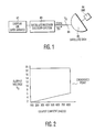
- FIG. 1 A block diagram of a typical satellite receiver system is depicted in Figure 1 .
- the receiver system includes an outdoor microwave antenna 85 which can be aimed at a satellite to receive a signal from a satellite.
- the signal received from the satellite is amplified by a conventional low noise block converter (LNB) 86 mounted in very close proximity to or on the antenna.
- LNB 86 down-converts satellite signals at high frequencies, typically in the gigahertz range, to signals at frequencies in the high megahertz range.
- An output signal from LNB 86 is carried to an indoor satellite receiver and decoder system 83 by a coaxial cable 84, decoded and presented with a monitor device 81.
- LNB low noise block converter
- a direct current (DC) output supply voltage V o is multiplexed onto the center conductor of coaxial cable 84.
- Voltage V o has a level that is, selectively, either 13V or 18V.
- the power supply, not shown, may include a series pass transistor.
- An example of a prior art power supply that generates output supply voltage similar to voltage V o is described in United States Patent No. 5,563,500 , entitled VOLTAGE REGULATOR HAVING COMPLEMENTARY TYPE TRANSISTOR in the name of Muterspaugh (the Muterspaugh Patent).
- the lower and higher output supply levels of voltage V o are used, selectively, to control polarization settings of LNB 86.
- the lower voltage level 13V selects right hand circular polarization (RHCP) and the higher voltage 18V selects left hand circular polarization (LHCP).
- LNB 86 of Figure 1 The circuits in LNB 86 of Figure 1 are designed to function properly when energized at either the lower output supply level 13V and the higher output supply level at 18V.
- a current drain IO of LNB 86 is about the same with either of the 13V level or the 18V level.
- Figure 2 illustrates a typical relationship between output supply voltage V o and output current 10 of the power supply, not shown, of the satellite receiver system of FIGURE 1 .
- the maximum power dissipation in the series pass transistor will occur when the voltage difference between the input and output main current conducting terminals of the series pass transistor, not shown, is at the maximum and the output current is at the maximum. This condition will occur at the 6 volt level of FIGURE 2 .
- the controllable series pass transistor may be damaged if a short circuit or other fault is formed at the output terminal of the series pass transistor.
- a fault condition may be a result of, for example, improper wiring the output of the receiving instrument. Examples of improper wiring include driving a nail through the coax cable and connecting of the satellite receiver to a conventional roof antenna instead of the satellite dish. Such damage often is caused by excessive thermal dissipation of the series pass transistor or by exceeding the current rating of the series pass transistor. For this reason, it is common to provide overload protection to prevent such damage to the series pass transistor.
- Another prior art includes a dual input supply voltage of arrangement.
- a higher output voltage of 22 volts is developed at an input, main current conducting terminal of the series pass transistor, not shown.
- a lower input supply voltage at 16 volts is developed at the input main current conducting terminal of the series pass transistor, not shown.
- United States Patent No. 5,893,023 entitled “Satellite receiver including operating voltage supply arrangement suitable for different antenna assemblies", discloses a satellite receiver which is capable of being connected to different antenna assemblies which require different operating voltages.
- the receiver includes a switch mode power supply which supplies the different operating voltages.
- a microprocessor controls the duty cycle of the switch mode power supply to produce the different operating voltages in accordance with the required duty cycle.
- a memory stores values which define different duty cycles for each of the operating voltages and provides the values to the microprocessor.
- a power supply embodying an inventive feature, includes the aforementioned dual input supply voltage arrangement.
- a comparator senses a magnitude of an output voltage produced by the series pass transistor. When, as a result of an over current condition, the output voltage becomes lower than a reference threshold level, any attempt to select the higher output voltage of 18V is automatically over-ridden and the lower input supply voltage, instead, is developed at the input main current conducting terminal of the series pass transistor, not shown. This action, advantageously, decreases the maximum amount of power that the series pass transistor dissipates.
- a power supply for a communication apparatus includes, a source of a first control signal that is indicative when a first antenna signal is to be selected and when a second antenna signal is to be selected.
- a power transistor is responsive to the first control signal for generating an output supply voltage at a value selected in accordance with the first control signal.
- the output supply voltage is coupled to a stage of the communication apparatus to select the first antenna signal, when a first value of the output supply voltage is generated and the second antenna signal, when a second value of said output supply voltage is generated.
- a switch is responsive to the first control signal and coupled to an input of the power transistor for selecting, in a first switching state of the switch, a first input supply voltage to be developed at the input, when the first antenna signal is selected.
- a second input supply voltage is selected to be developed at the input, when the second antenna signal is selected.
- a fault detector is coupled to the switch for changing the switching state in the switch, when the second antenna signal is selected and a fault condition occurs, to select an input supply voltage to be developed at the input that is different from the second input supply voltage.
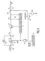
- FIGURE 3 illustrates a power supply regulator 10, embodying an inventive feature, is used to energize a low noise block converter (LNB) 86 of FIGURE 1 .
- Power supply regulator 10 of FIGURE 3 provides regulated output voltage V o at an output terminal 16.
- Terminal 16 is coupled to LNB 86 via coax cable 84 of FIGURE 1 .
- An emitter of a series pass power transistor Q1 of FIGURE 3 is supplied with an input voltage V IN higher than regulated output voltage V o , developed at terminal 16.
- a collector of transistor Q1 is coupled via a current sensing resistor 20 to terminal 16.
- An LNB voltage control circuit 7 senses output voltage V o and controls power transistor Q1 for regulating output voltage V o .
- a level of output voltage V o is selected by a bi-level or binary control signal 23c at a control terminal 53.
- a comparator 22 embodying an inventive feature, having a corresponding reference voltage 22a, produces an output signal 23a at a TRUE state.
- Reference voltage 22a establishes the threshold level of comparator 22. Consequently, a signal 23c produced by an AND gate 23 is at the same state as that of an output signal 23b produced by a microprocessor 41.
- signal 23c can selectively assume either a TRUE state, for selecting output voltage V o at 18V, or a FALSE state, for selecting output voltage V o at 13V, in accordance with signal 23b of microprocessor 41.
- the lower voltage level 13V of output voltage V o selects right hand circular polarization (RHCP) and the higher voltage 18V of output voltage V o selects left hand circular polarization (LHCP).
- RHCP right hand circular polarization
- LHCP left hand circular polarization
- FIGURE 3 also illustrates a dual input supply voltage arrangement 200 for generating input voltage V IN that energizes LNB power supply regulator 10.
- a metal oxide semiconductor field effect transistor (MOSFET) 51 operating as a switch, is turned on by signal 23c to supply input voltage V IN at 22 volts to the emitter of transistor Q1 from an input supply voltage 301.
- MOSFET 51 is turned off by signal 23c. Consequently, input voltage V IN at approximately 16 volts is supplied to the emitter of input voltage V IN via an anode terminal of diode 21.
- transistor Q1 via a diode 21.
- diode 21 and MOSFET 51 form an input voltage selection switch for a dual voltage power supply.
- power supply regulator 10 In normal operation, power supply regulator 10 generates output voltage V o at the 18 volt level from input voltage V IN at approximately 22 volts. Similarly, power supply regulator 10 generates output voltage V o at the 13 volt level from input voltage V IN at approximately 16 volts.
- An LNB similar to LNB 86 of FIGURE 1 , includes an internal power supply regulator, not shown, for generating an internal supply voltage of 5V, not shown, from voltage V o at either the 13V level or the 18V level.
- the internal power supply regulator not shown, requires a minimum input supply voltage of 6V for producing the 5V level that is capable of providing the maximum required LNB operation current.
- a maximum LNB operation current can be produced when voltage V o at at least 6 volts level is applied to LNB 86.
- power supply regulator 10 of FIGURE 3 is designed to supply a maximum current level of an output current I o when output supply voltage V o is equal to or greater than 6 volt.
- the relationship between output supply voltage Vo and an output current I o are shown in FIGURE 2 , as explained before.
- the maximum power dissipation in transistor Q1 of FIGURE 3 occurs when voltage Vo is equal to 6V and output current I o is at the current limit level. If not prevented from doing so, the decrease in output voltage V o would cause the voltage drop develop between the emitter and collector of power transistor Q1 to become excessive when input voltage V IN at 22 volts is coupled to the emitter of transistor Q1. The additional heat generated in such fault condition could prematurely produce a permanent damage to power transistor Q1.
- output signal 23a of comparator 22 of FIGURE 3 is at a LOW state.
- output signal 23a comparator 22 is at the LOW state, it over-rides, by the operation of AND gate 23, the operation of selection signal 23b.
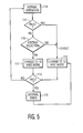
- power supply regulator 10 is forced to operate in a 13V mode in which output voltage V o is 13V, as depicted in a step 92 of the flow chart of FIGURE 4 , regardless of selection signal 23b produced by microprocessor 41.
- MOSFET 51 is turned off by signal 23b to supply, via diode 21, input voltage V IN at approximately 16 volts at the emitter of power transistor Q1. This action, advantageously, decreases the amount of power that power transistor Q1 needs to dissipate.
- the threshold level established by voltage 22a is preferably selected to be lower than the lower voltage level 13V of output voltage V o , and higher than 6 volts.
- signal 23a of FIGURE 3 is coupled to microprocessor 41, as shown by the broken line.
- Signal 23b of microprocessor 41 is passed to terminal 53.
- Microprocessor 41 monitors signal 23a.
- output signal 23a of comparator 22 is at the LOW state, indicating a fault condition, as determined in step 111 of FIGURE 5
- microprocessor 41 of FIGURE 3 unconditionally generates signal 23b at the LOW state. Therefore, power supply regulator 10 is forced to operate in the 13 volt mode, in a manner described before, as depicted in step 112 of FIGURE 5 .
- step 114 When the fault condition disappears, as depicted in step 113 of FIGURE 5 , normal operation step 114 can resume. On the other hand, if the fault persists, an interval timer step 115 will maintain the 13 volt mode. If fault is not detected in step 111, microprocessor 41 of FIGURE 3 selectively generates signal 23b at the LOW state or at the HIGH state in a step 116. Signal 23b of FIGURE 3 at the HIGH state will cause power supply regulator 10 to operate in the 18 volt mode in which output voltage V o is 18V, in a manner described before, as depicted in step 117 of FIGURE 5 .
- FIGURE 6 illustrates a power supply regulator 10', embodying an inventive feature, that is used to energize LNB 86 of FIGURE 1 . Similar symbols in FIGUREs 3 and 6 indicate similar items or functions.
- Power supply regulator 10' of FIGURE 6 is intended to provide additional advantages, for example operating with fewer parts at a lower cost and protecting power transistor Q1' against thermal damage from excess heat dissipation. These advantages are achieved by eliminating the dual input supply voltage and, instead, switching a power resistor 310' into and out of a series coupling with power transistor Q1'. Resistor 310' is coupled between a main current conducting terminal 51 a' and a main current conducting terminal 51b'. The differences between the arrangements of FIGUREs 3 and 6 will be described in detail; the remaining operation being substantially the same.
- a single input supply voltage 301' is provided, namely the 22 volt supply.
- Power resistor 310' is used to absorb the additional heat generated in the lower 13 volt mode, when the lower level of 13 volts of output voltage V o is selected.
- Power resistor 310' can be implemented, for example, by using two resistors coupled across the main current conducting terminals 51a' and 51b' of MOSFET 51' and having an equivalent value of 9 Ohm.
- circuit 10 of Figure 3 employs diode 21 and MOSFET 51 to switch voltage V IN to the 16 volt level, in a fault condition and when the lower level of 13 volts of output voltage V o is selected.
- MOSFET 51' causes power resistor 310' to be coupled in series with transistor Q1', both in a fault condition and when the lower level of 13 volts of output voltage V o is selected.
Landscapes
- Engineering & Computer Science (AREA)
- Signal Processing (AREA)
- Computer Networks & Wireless Communication (AREA)
- Physics & Mathematics (AREA)
- Astronomy & Astrophysics (AREA)
- General Physics & Mathematics (AREA)
- Input Circuits Of Receivers And Coupling Of Receivers And Audio Equipment (AREA)
- Continuous-Control Power Sources That Use Transistors (AREA)
Applications Claiming Priority (3)
| Application Number | Priority Date | Filing Date | Title |
|---|---|---|---|
| US37001602P | 2002-04-03 | 2002-04-03 | |
| US370016P | 2002-04-03 | ||
| PCT/US2003/010283 WO2003085850A1 (en) | 2002-04-03 | 2003-04-03 | Power supply for a satellite receiver |
Publications (3)
| Publication Number | Publication Date |
|---|---|
| EP1490979A1 EP1490979A1 (en) | 2004-12-29 |
| EP1490979A4 EP1490979A4 (en) | 2011-05-04 |
| EP1490979B1 true EP1490979B1 (en) | 2015-08-12 |
Family
ID=28792017
Family Applications (1)
| Application Number | Title | Priority Date | Filing Date |
|---|---|---|---|
| EP03746133.2A Expired - Lifetime EP1490979B1 (en) | 2002-04-03 | 2003-04-03 | Power supply for a satellite receiver |
Country Status (7)
| Country | Link |
|---|---|
| EP (1) | EP1490979B1 (enExample) |
| JP (1) | JP4369759B2 (enExample) |
| KR (1) | KR20040105835A (enExample) |
| CN (1) | CN1643800B (enExample) |
| AU (1) | AU2003226246A1 (enExample) |
| MX (1) | MXPA04009706A (enExample) |
| WO (1) | WO2003085850A1 (enExample) |
Families Citing this family (4)
| Publication number | Priority date | Publication date | Assignee | Title |
|---|---|---|---|---|
| KR100655972B1 (ko) * | 2004-10-22 | 2006-12-11 | 엘지전자 주식회사 | 지피에스 전원관리 기능을 갖는 이동통신 단말기 및 그 방법 |
| CN101268694B (zh) | 2005-09-19 | 2011-11-09 | 汤姆逊许可证公司 | 用于依赖通信模式/协议的lnb电源输出的自适应阻抗 |
| CN104570853B (zh) * | 2014-12-18 | 2017-04-05 | 中国科学院长春光学精密机械与物理研究所 | 高可靠组合智能空间电源系统 |
| CN104767948B (zh) * | 2015-04-10 | 2017-12-01 | 无锡市晶源微电子有限公司 | 一种卫星接收高频头lnb偏置电路 |
Family Cites Families (6)
| Publication number | Priority date | Publication date | Assignee | Title |
|---|---|---|---|---|
| GB9008898D0 (en) * | 1990-04-20 | 1990-06-20 | Ferguson Ltd | Receiver for satellite reception |
| US5563500A (en) * | 1994-05-16 | 1996-10-08 | Thomson Consumer Electronics, Inc. | Voltage regulator having complementary type transistor |
| US5787336A (en) * | 1994-11-08 | 1998-07-28 | Space Systems/Loral, Inc. | Satellite communication power management system |
| FR2728408B1 (fr) * | 1994-12-20 | 1997-01-31 | Alsthom Cge Alcatel | Dispositif d'alimentation electrique notamment pour appareils portatifs |
| JP2925470B2 (ja) * | 1995-03-17 | 1999-07-28 | 東光株式会社 | 直列制御形レギュレータ |
| CN1147139C (zh) * | 1998-02-16 | 2004-04-21 | 皇家菲利浦电子有限公司 | 卫星接收机 |
-
2003
- 2003-04-03 CN CN038073250A patent/CN1643800B/zh not_active Expired - Fee Related
- 2003-04-03 EP EP03746133.2A patent/EP1490979B1/en not_active Expired - Lifetime
- 2003-04-03 KR KR10-2004-7015618A patent/KR20040105835A/ko not_active Abandoned
- 2003-04-03 MX MXPA04009706A patent/MXPA04009706A/es active IP Right Grant
- 2003-04-03 JP JP2003582921A patent/JP4369759B2/ja not_active Expired - Fee Related
- 2003-04-03 WO PCT/US2003/010283 patent/WO2003085850A1/en not_active Ceased
- 2003-04-03 AU AU2003226246A patent/AU2003226246A1/en not_active Abandoned
Also Published As
| Publication number | Publication date |
|---|---|
| CN1643800B (zh) | 2010-05-26 |
| JP2005522142A (ja) | 2005-07-21 |
| EP1490979A4 (en) | 2011-05-04 |
| MXPA04009706A (es) | 2005-01-11 |
| AU2003226246A1 (en) | 2003-10-20 |
| KR20040105835A (ko) | 2004-12-16 |
| JP4369759B2 (ja) | 2009-11-25 |
| EP1490979A1 (en) | 2004-12-29 |
| WO2003085850A1 (en) | 2003-10-16 |
| CN1643800A (zh) | 2005-07-20 |
Similar Documents
| Publication | Publication Date | Title |
|---|---|---|
| EP1239573B1 (en) | Overvoltage-protective device for power system, AC/DC converter and DC/DC converter constituting the power system | |
| US6996389B2 (en) | Power supply for a satellite receiver | |
| US6147545A (en) | Bridge control circuit for eliminating shoot-through current | |
| US6369460B1 (en) | Power supply monitoring apparatus for vehicle | |
| US20040251884A1 (en) | High efficiency off-line linear power supply | |
| US8502513B2 (en) | Voltage regulator | |
| US6411483B1 (en) | Hiccup-mode current protection circuit for switching regulator | |
| US8384366B2 (en) | System and method for providing stable control for power systems | |
| EP0763224B1 (en) | Voltage regulator | |
| EP3192140B1 (en) | Protective circuit | |
| EP0151856B1 (en) | Power on-off control circuit | |
| EP1490979B1 (en) | Power supply for a satellite receiver | |
| HU225080B1 (en) | Voltage regulator arrangement | |
| WO2007100327A1 (en) | Method for regulating a voltage and circuit therefor | |
| US20130134801A1 (en) | Power supply circuit for antenna, antenna control system, and digital communication device | |
| JP2001136657A (ja) | 電子機器の電源回路 | |
| EP0794604A2 (en) | Overcurrent protector | |
| US20060028079A1 (en) | Backup battery charging circuit | |
| US7259596B2 (en) | Circuit arrangement for monitoring a voltage | |
| CN220291729U (zh) | 电源切换电路 | |
| US20060018071A1 (en) | Protective device for antenna power circuit | |
| KR100294573B1 (ko) | 스위칭식 lnb 구동용 전원 모듈 장치 | |
| US6522512B1 (en) | Anti-latch-up circuit | |
| JPH11136850A (ja) | 過電流防止回路 | |
| JP2006101595A (ja) | 2系統電源用電圧検知回路 |
Legal Events
| Date | Code | Title | Description |
|---|---|---|---|
| PUAI | Public reference made under article 153(3) epc to a published international application that has entered the european phase |
Free format text: ORIGINAL CODE: 0009012 |
|
| 17P | Request for examination filed |
Effective date: 20040922 |
|
| AK | Designated contracting states |
Kind code of ref document: A1 Designated state(s): AT BE BG CH CY CZ DE DK EE ES FI FR GB GR HU IE IT LI LU MC NL PT RO SE SI SK TR |
|
| AX | Request for extension of the european patent |
Extension state: AL LT LV MK |
|
| RIN1 | Information on inventor provided before grant (corrected) |
Inventor name: LELEY, SURESH, VISHWANATM Inventor name: FITZPATRICK, JOHN, JAMES Inventor name: BOWYER, ANDREW, ERIC Inventor name: CURTIS, III, JOHN, JOSEPH Inventor name: PITSCH, ROBERT, ALAN |
|
| RAP1 | Party data changed (applicant data changed or rights of an application transferred) |
Owner name: THOMSON LICENSING |
|
| RAP1 | Party data changed (applicant data changed or rights of an application transferred) |
Owner name: THOMSON LICENSING |
|
| A4 | Supplementary search report drawn up and despatched |
Effective date: 20110405 |
|
| 17Q | First examination report despatched |
Effective date: 20110609 |
|
| REG | Reference to a national code |
Ref country code: DE Ref legal event code: R079 Ref document number: 60347915 Country of ref document: DE Free format text: PREVIOUS MAIN CLASS: H04B0001060000 Ipc: H04B0001180000 |
|
| GRAP | Despatch of communication of intention to grant a patent |
Free format text: ORIGINAL CODE: EPIDOSNIGR1 |
|
| RIC1 | Information provided on ipc code assigned before grant |
Ipc: H04H 40/90 20080101ALI20150209BHEP Ipc: H04B 1/18 20060101AFI20150209BHEP |
|
| INTG | Intention to grant announced |
Effective date: 20150304 |
|
| GRAS | Grant fee paid |
Free format text: ORIGINAL CODE: EPIDOSNIGR3 |
|
| GRAA | (expected) grant |
Free format text: ORIGINAL CODE: 0009210 |
|
| AK | Designated contracting states |
Kind code of ref document: B1 Designated state(s): DE FR GB IT |
|
| REG | Reference to a national code |
Ref country code: GB Ref legal event code: FG4D |
|
| REG | Reference to a national code |
Ref country code: DE Ref legal event code: R084 Ref document number: 60347915 Country of ref document: DE |
|
| REG | Reference to a national code |
Ref country code: DE Ref legal event code: R096 Ref document number: 60347915 Country of ref document: DE |
|
| REG | Reference to a national code |
Ref country code: FR Ref legal event code: PLFP Year of fee payment: 14 |
|
| PG25 | Lapsed in a contracting state [announced via postgrant information from national office to epo] |
Ref country code: IT Free format text: LAPSE BECAUSE OF FAILURE TO SUBMIT A TRANSLATION OF THE DESCRIPTION OR TO PAY THE FEE WITHIN THE PRESCRIBED TIME-LIMIT Effective date: 20150812 |
|
| REG | Reference to a national code |
Ref country code: DE Ref legal event code: R097 Ref document number: 60347915 Country of ref document: DE |
|
| PLBE | No opposition filed within time limit |
Free format text: ORIGINAL CODE: 0009261 |
|
| STAA | Information on the status of an ep patent application or granted ep patent |
Free format text: STATUS: NO OPPOSITION FILED WITHIN TIME LIMIT |
|
| 26N | No opposition filed |
Effective date: 20160513 |
|
| GBPC | Gb: european patent ceased through non-payment of renewal fee |
Effective date: 20160403 |
|
| PG25 | Lapsed in a contracting state [announced via postgrant information from national office to epo] |
Ref country code: GB Free format text: LAPSE BECAUSE OF NON-PAYMENT OF DUE FEES Effective date: 20160403 |
|
| REG | Reference to a national code |
Ref country code: FR Ref legal event code: PLFP Year of fee payment: 15 |
|
| REG | Reference to a national code |
Ref country code: DE Ref legal event code: R082 Ref document number: 60347915 Country of ref document: DE Representative=s name: DEHNS, DE Ref country code: DE Ref legal event code: R082 Ref document number: 60347915 Country of ref document: DE Representative=s name: HOFSTETTER, SCHURACK & PARTNER PATENT- UND REC, DE |
|
| REG | Reference to a national code |
Ref country code: FR Ref legal event code: PLFP Year of fee payment: 16 |
|
| REG | Reference to a national code |
Ref country code: FR Ref legal event code: TP Owner name: THOMSON LICENSING DTV, FR Effective date: 20180830 |
|
| REG | Reference to a national code |
Ref country code: DE Ref legal event code: R082 Ref document number: 60347915 Country of ref document: DE Representative=s name: DEHNS, DE Ref country code: DE Ref legal event code: R081 Ref document number: 60347915 Country of ref document: DE Owner name: INTERDIGITAL MADISON PATENT HOLDINGS, FR Free format text: FORMER OWNER: THOMSON LICENSING, ISSY-LES-MOULINEAUX, FR |
|
| PGFP | Annual fee paid to national office [announced via postgrant information from national office to epo] |
Ref country code: FR Payment date: 20190325 Year of fee payment: 17 |
|
| PGFP | Annual fee paid to national office [announced via postgrant information from national office to epo] |
Ref country code: DE Payment date: 20190220 Year of fee payment: 17 |
|
| REG | Reference to a national code |
Ref country code: DE Ref legal event code: R119 Ref document number: 60347915 Country of ref document: DE |
|
| PG25 | Lapsed in a contracting state [announced via postgrant information from national office to epo] |
Ref country code: FR Free format text: LAPSE BECAUSE OF NON-PAYMENT OF DUE FEES Effective date: 20200430 Ref country code: DE Free format text: LAPSE BECAUSE OF NON-PAYMENT OF DUE FEES Effective date: 20201103 |