EP1489698A2 - Vorrichtung und Verfahren zum elektrischen Verbinden eines elektrischen Leiters mit einem elektronischen Bauelement - Google Patents
Vorrichtung und Verfahren zum elektrischen Verbinden eines elektrischen Leiters mit einem elektronischen Bauelement Download PDFInfo
- Publication number
- EP1489698A2 EP1489698A2 EP04012942A EP04012942A EP1489698A2 EP 1489698 A2 EP1489698 A2 EP 1489698A2 EP 04012942 A EP04012942 A EP 04012942A EP 04012942 A EP04012942 A EP 04012942A EP 1489698 A2 EP1489698 A2 EP 1489698A2
- Authority
- EP
- European Patent Office
- Prior art keywords
- contacting device
- section
- conductor
- contact
- textile material
- Prior art date
- Legal status (The legal status is an assumption and is not a legal conclusion. Google has not performed a legal analysis and makes no representation as to the accuracy of the status listed.)
- Withdrawn
Links
Images


Classifications
-
- D—TEXTILES; PAPER
- D03—WEAVING
- D03D—WOVEN FABRICS; METHODS OF WEAVING; LOOMS
- D03D15/00—Woven fabrics characterised by the material, structure or properties of the fibres, filaments, yarns, threads or other warp or weft elements used
-
- D—TEXTILES; PAPER
- D03—WEAVING
- D03D—WOVEN FABRICS; METHODS OF WEAVING; LOOMS
- D03D1/00—Woven fabrics designed to make specified articles
- D03D1/0088—Fabrics having an electronic function
-
- D—TEXTILES; PAPER
- D03—WEAVING
- D03D—WOVEN FABRICS; METHODS OF WEAVING; LOOMS
- D03D15/00—Woven fabrics characterised by the material, structure or properties of the fibres, filaments, yarns, threads or other warp or weft elements used
- D03D15/50—Woven fabrics characterised by the material, structure or properties of the fibres, filaments, yarns, threads or other warp or weft elements used characterised by the properties of the yarns or threads
- D03D15/593—Stiff materials, e.g. cane or slat
-
- H—ELECTRICITY
- H01—ELECTRIC ELEMENTS
- H01R—ELECTRICALLY-CONDUCTIVE CONNECTIONS; STRUCTURAL ASSOCIATIONS OF A PLURALITY OF MUTUALLY-INSULATED ELECTRICAL CONNECTING ELEMENTS; COUPLING DEVICES; CURRENT COLLECTORS
- H01R12/00—Structural associations of a plurality of mutually-insulated electrical connecting elements, specially adapted for printed circuits, e.g. printed circuit boards [PCB], flat or ribbon cables, or like generally planar structures, e.g. terminal strips, terminal blocks; Coupling devices specially adapted for printed circuits, flat or ribbon cables, or like generally planar structures; Terminals specially adapted for contact with, or insertion into, printed circuits, flat or ribbon cables, or like generally planar structures
- H01R12/50—Fixed connections
- H01R12/51—Fixed connections for rigid printed circuits or like structures
- H01R12/515—Terminal blocks providing connections to wires or cables
-
- H—ELECTRICITY
- H01—ELECTRIC ELEMENTS
- H01R—ELECTRICALLY-CONDUCTIVE CONNECTIONS; STRUCTURAL ASSOCIATIONS OF A PLURALITY OF MUTUALLY-INSULATED ELECTRICAL CONNECTING ELEMENTS; COUPLING DEVICES; CURRENT COLLECTORS
- H01R12/00—Structural associations of a plurality of mutually-insulated electrical connecting elements, specially adapted for printed circuits, e.g. printed circuit boards [PCB], flat or ribbon cables, or like generally planar structures, e.g. terminal strips, terminal blocks; Coupling devices specially adapted for printed circuits, flat or ribbon cables, or like generally planar structures; Terminals specially adapted for contact with, or insertion into, printed circuits, flat or ribbon cables, or like generally planar structures
- H01R12/50—Fixed connections
- H01R12/59—Fixed connections for flexible printed circuits, flat or ribbon cables or like structures
- H01R12/592—Fixed connections for flexible printed circuits, flat or ribbon cables or like structures connections to contact elements
-
- H—ELECTRICITY
- H05—ELECTRIC TECHNIQUES NOT OTHERWISE PROVIDED FOR
- H05K—PRINTED CIRCUITS; CASINGS OR CONSTRUCTIONAL DETAILS OF ELECTRIC APPARATUS; MANUFACTURE OF ASSEMBLAGES OF ELECTRICAL COMPONENTS
- H05K3/00—Apparatus or processes for manufacturing printed circuits
- H05K3/30—Assembling printed circuits with electric components, e.g. with resistor
- H05K3/32—Assembling printed circuits with electric components, e.g. with resistor electrically connecting electric components or wires to printed circuits
- H05K3/325—Assembling printed circuits with electric components, e.g. with resistor electrically connecting electric components or wires to printed circuits by abutting or pinching, i.e. without alloying process; mechanical auxiliary parts therefor
- H05K3/326—Assembling printed circuits with electric components, e.g. with resistor electrically connecting electric components or wires to printed circuits by abutting or pinching, i.e. without alloying process; mechanical auxiliary parts therefor the printed circuit having integral resilient or deformable parts, e.g. tabs or parts of flexible circuits
-
- D—TEXTILES; PAPER
- D10—INDEXING SCHEME ASSOCIATED WITH SUBLASSES OF SECTION D, RELATING TO TEXTILES
- D10B—INDEXING SCHEME ASSOCIATED WITH SUBLASSES OF SECTION D, RELATING TO TEXTILES
- D10B2401/00—Physical properties
- D10B2401/16—Physical properties antistatic; conductive
-
- H—ELECTRICITY
- H05—ELECTRIC TECHNIQUES NOT OTHERWISE PROVIDED FOR
- H05K—PRINTED CIRCUITS; CASINGS OR CONSTRUCTIONAL DETAILS OF ELECTRIC APPARATUS; MANUFACTURE OF ASSEMBLAGES OF ELECTRICAL COMPONENTS
- H05K2201/00—Indexing scheme relating to printed circuits covered by H05K1/00
- H05K2201/05—Flexible printed circuits [FPCs]
- H05K2201/055—Folded back on itself
-
- H—ELECTRICITY
- H05—ELECTRIC TECHNIQUES NOT OTHERWISE PROVIDED FOR
- H05K—PRINTED CIRCUITS; CASINGS OR CONSTRUCTIONAL DETAILS OF ELECTRIC APPARATUS; MANUFACTURE OF ASSEMBLAGES OF ELECTRICAL COMPONENTS
- H05K2201/00—Indexing scheme relating to printed circuits covered by H05K1/00
- H05K2201/09—Shape and layout
- H05K2201/09009—Substrate related
- H05K2201/09081—Tongue or tail integrated in planar structure, e.g. obtained by cutting from the planar structure
-
- H—ELECTRICITY
- H05—ELECTRIC TECHNIQUES NOT OTHERWISE PROVIDED FOR
- H05K—PRINTED CIRCUITS; CASINGS OR CONSTRUCTIONAL DETAILS OF ELECTRIC APPARATUS; MANUFACTURE OF ASSEMBLAGES OF ELECTRICAL COMPONENTS
- H05K2201/00—Indexing scheme relating to printed circuits covered by H05K1/00
- H05K2201/10—Details of components or other objects attached to or integrated in a printed circuit board
- H05K2201/10227—Other objects, e.g. metallic pieces
- H05K2201/10287—Metal wires as connectors or conductors
-
- H—ELECTRICITY
- H05—ELECTRIC TECHNIQUES NOT OTHERWISE PROVIDED FOR
- H05K—PRINTED CIRCUITS; CASINGS OR CONSTRUCTIONAL DETAILS OF ELECTRIC APPARATUS; MANUFACTURE OF ASSEMBLAGES OF ELECTRICAL COMPONENTS
- H05K3/00—Apparatus or processes for manufacturing printed circuits
- H05K3/30—Assembling printed circuits with electric components, e.g. with resistor
- H05K3/32—Assembling printed circuits with electric components, e.g. with resistor electrically connecting electric components or wires to printed circuits
- H05K3/321—Assembling printed circuits with electric components, e.g. with resistor electrically connecting electric components or wires to printed circuits by conductive adhesives
-
- H—ELECTRICITY
- H05—ELECTRIC TECHNIQUES NOT OTHERWISE PROVIDED FOR
- H05K—PRINTED CIRCUITS; CASINGS OR CONSTRUCTIONAL DETAILS OF ELECTRIC APPARATUS; MANUFACTURE OF ASSEMBLAGES OF ELECTRICAL COMPONENTS
- H05K3/00—Apparatus or processes for manufacturing printed circuits
- H05K3/30—Assembling printed circuits with electric components, e.g. with resistor
- H05K3/32—Assembling printed circuits with electric components, e.g. with resistor electrically connecting electric components or wires to printed circuits
- H05K3/328—Assembling printed circuits with electric components, e.g. with resistor electrically connecting electric components or wires to printed circuits by welding
Definitions
- the invention relates to a contacting device for electrical connection of an electrical conductor to a electronic component according to claim 1, an electronic Component according to claim 6 and a method according to claim 7th
- the contacting of the conductive wires with the metallized pads on them connecting circuit board 4 by thermal connection of a Sandwich structure realized.
- the contacting process according to the The prior art is shown in FIG. 5.
- the stripped fiber 1 placed on the metal pad 2 and a Metallic counterpart 3 is on the metal pad 2 corresponding position on the other side of the stripped Fiber 1 laid on.
- the metal pad 2 and that metallic counterpart 3 by thermal connection connected with each other are Disadvantages that the stripped point 1 of the conductive tissue be adjusted with respect to the metal pads 2 of the circuit board 4 must and that for each connection a metallic counterpart 3 put on and must also be adjusted.
- the movable section is preferably designed such that that during the process of electrical connection to the immovable section can be folded.
- the movable section and the immovable section of the Contacts can be considered as separate units or as interconnected units can be formed.
- the electronic component can be, for example an integrated circuit (chip) or one on one Insulator applied conductor track, which with an external electronic component is connected, act.
- the textile material is preferably a woven fabric.
- Under a Tissue becomes a textile fabric made up of two especially understood at right angles crossing thread systems, which - as usual - are called warp and weft.
- the warp lies in the longitudinal direction of the weaving process Weft direction is transverse to the weaving direction.
- the conductor preferably comprises at least one shot and / or Warp thread of the fabric.
- the movable section and / or the immovable portion of the contact covered area of the A recess or an opening or a substrate material Hole is provided in the substrate material. So are the movable section and / or the immovable section of the Contact exposed by the substrate material.
- the recess in the substrate material is special advantageous if the movable section, the immovable Section and the conductor in a thermocompression step, such as. Solder, be electrically connected to each other.
- thermocompression device This can go through the exposed area of the contact directly be contacted with the thermocompression device. Consequently better heat transfer is made possible.
- the movable section and the immovable section are preferred Section joined together.
- Junction between the movable section and the immovable section of the point or axis about which of the movable section is moved when it is on the immovable Section is folded.
- the movable section and the immovable one Section formed in one piece.
- At least one conductor track is also on or on the substrate material, which with the at least a contact is electrically connected.
- the contact can be made in a simple and advantageous manner e.g. be connected to a component to be connected.
- an electronic component is also provided which a contacting device according to the Invention or a preferred embodiment thereof.
- the step of electrically connecting comprises a step of at least partially heating or heating of the contact or a thermocompression step.
- the method can preferably also include a step of thermal welding and / or gluing the Include contacting device and the textile material.
- the method further preferably comprises a step of at least area-wise application or lamination of one insulating layer or adhesive layer on the Contacting device and the textile material, which are interconnected according to the invention.
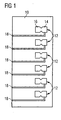
- the manufacturing process is first Contacting device according to the first preferred Embodiment of the present invention with reference to Figs. 1 and 2A.
- contacts 12 are made on a substrate material 10 applied or arranged or trained.
- the embodiment shown is six contacts 12 provided, however, any other required number of Contacts 12 can be provided.
- the contacts 12 point two sections 14, 16, the section 14 in the completed contacting an immobile Section 14 forms and section 16 a movable Section 16 trains.
- the sections 14, 16 are integrally connected to one another educated. Alternatively, however, it is conceivable that the sections 14, 16 are spatially separated, i.e. Not are interconnected.
- interconnects 18 are formed on the substrate material formed, each with a contact 12 electrically are connected and preferably serve the Contacting device with a (not shown) to connect electronic component.
- a next process step becomes the substrate material below the movable section 16 by e.g. Lasers, etching, etc., removed.
- the movable section 16 in substantially completely freed from the substrate material 10 or exposed and can thus be moved.
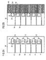
- the textile material 30 is preferably a woven fabric.
- a fabric is formed from two textile surfaces thread systems crossing each other at right angles understood which - as usual - as a warp and a weft be designated.
- the chain lies in the longitudinal direction of the Weaving process during the weft direction transverse to the weaving direction runs.
- FIG Embodiment In the textile material 30 are shown in FIG Embodiment six conductors 32 woven.
- a conductor 32 consists of several im essentially parallel to each other electrically conductive wires or fibers 34, which preferably of an electrically insulating jacket or Isolation (not shown) are surrounded.
- the conductor 32 is contacted at the point to be contacted the insulation of the wire 34 removed so that the inner conductor exposed.
- the textile material 30 prepared in this way is combined with the Conductors 32 arranged on the contacting device such that the immovable portions 14 of the contacts 12 essentially covered by the conductors 32.
- the movable portion 16 of the contact 12 folded over and now covers the conductor 32.
- the textile material 30 and the conductors 32 woven therein become substantially between those now essentially opposite each other Sections 14, 16 of the contact 12 held and positioned.
- thermocompression step in which the warmth or heat on the exposed movable section 16 can be applied a good bond between the contact 12 and the conductor 32 are formed.
- the Contact 12 on the side facing the textile material 30 be provided with a soldering agent, preferably solder, which during the thermocompression step into the textile Penetrates material and thus a stable electrical and mechanical connection.
- soldering agent preferably solder
- a conductive adhesive can be used instead of Solder.
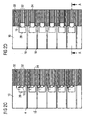
- a contacting device according to the second preferred embodiment of the present invention With reference to Figs. 3A to 3D.
- the manufacturing process becomes a Contacting device according to the second preferred Embodiment described with reference to FIGS. 1 and 3A.
- Fig. 1 Similar to that described in the first embodiment, an arrangement as shown in Fig. 1 is formed.
- the substrate material 10 is below the immovable portion 14 of the contact 12 removed.
- This is 3A by the dashed box with reference numeral 42 indicated.
- it is essentially extensive movable section 16 made a cut so that the movable section 16 from the substrate material plane can be folded down or folded out. This is in Fig. 3A indicated by reference numeral 40.
- a textile Material 30 in which a conductor 32 is woven and at which the ends of the conductors 32 were stripped on the Contacting device arranged.
- the movable section 16 is on the immovable section 14 and the textile Material 30 folded down (Fig. 3C).
- sections 14, 16 of the Contact 12 electrically connected to the textile material 30.
- the heat or warmth through the recess 42 in the substrate material 10 below of the immovable portion 14 of the contact 12 is supplied.
- the electrical connection can be carried out similarly to described with respect to the first embodiment.
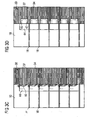
- the contacting device, the textile Material 30 and the conductor 32 at least in some areas coated on both sides with an insulator 50.
- an insulator 50 Through the Additional coating can be used to counter the contacts the penetration of dirt and moisture are protected, on the other hand, a better mechanical hold between the textile material 30 and the contacting device become.
- the mechanical hold is additionally improves that the insulator 50, which on the top and Underside is present through the recess 20 and connects here.
- an insulator 50 can also be used be provided.
- the Contacting device in each case on an edge or side area of the textile material 30 arranged.
- the contacting device in a central region of the to arrange textile material 30. This is the insulation the conductor is removed at the points to be contacted and that cuts non-conductive textile material, so that the movable section 16 of contacts 12 through the textile Material can pass through.
- the Contacts 12 and all recesses 20, 42, 44 rotated by 90 °.
- the stripped conductor 32 can laterally with the Contacting device can be connected and not frontally, as in the illustrated embodiments.
Landscapes
- Engineering & Computer Science (AREA)
- Textile Engineering (AREA)
- Metallurgy (AREA)
- Manufacturing & Machinery (AREA)
- Microelectronics & Electronic Packaging (AREA)
- Switch Cases, Indication, And Locking (AREA)
- Coupling Device And Connection With Printed Circuit (AREA)
- Multi-Conductor Connections (AREA)
Abstract
Description
- ein Substratmaterial;
- zumindest einen Kontakt bzw. Kontaktpad bzw. metallischen Pad, welcher an bzw. auf dem Substratmaterial ausgebildet ist, zum elektrischen Verbinden des Leiters mit der Kontaktiereinrichtung;
- der Kontakt einen beweglichen bzw. klappbaren bzw. umklappbaren Abschnitt und einen unbeweglichen bzw. festgelegten bzw. festen Abschnitt umfaßt, und
- der bewegliche Abschnitt derart ausgebildet ist, daß er beim Vorgang des elektrischen Verbindens dem unbeweglichen Abschnitt flächenseitig im wesentlichen gegenüberliegend angeordnet werden kann.
- Bereitstellen eines textilen Materials, in welchem zumindest ein flexibler, draht- und/oder fadenartiger elektrischer Leiter angeordnet ist;
- Anordnen einer Kontaktiereinrichtung an einer Flächenseite des textilen Materials an der zu verbindenden Stelle des Leiters;
- Anordnen bzw. Umklappen des beweglichen Abschnitts der Kontaktiereinrichtung flächenseitig im wesentlichen gegenüberliegend zu dem unbeweglichen Abschnitt der Kontaktiereinrichtung;
- elektrisches Verbinden des Leiters mit der Kontaktierungseinrichtung.
- Fig. 1
- eine Draufsicht auf eine Kontaktiereinrichtung während des Herstellungsprozesses einer erfindungsgemäßen Kontaktiereinrichtung;
- Fig. 2A
- eine Kontaktiereinrichtung gemäß einer ersten bevorzugten Ausführungsform der vorliegenden Erfindung;
- Figs. 2B bis 2D
- den Verbindungsvorgang zwischen der in Fig. 2A gezeigten Kontaktiereinrichtung und in einem textilen Material angeordneten elektrischen Leitern,
- Fig. 3A
- eine Kontaktiereinrichtung gemäß einer zweiten bevorzugten Ausführungsform der vorliegenden Erfindung;
- Fig. 3B bis 3D
- den Verbindungsvorgang der in Fig. 3A gezeigten Kontaktiereinrichtung;
- Fig. 4
- eine Schnittansicht, welche einem Schnitt entsprechend Linie A-A von Fig. 2D entspricht, wobei die Kontaktiereinrichtung und das textile Gewebe zumindest bereichsweise ummantelt ist; und
- Fig. 5
- eine Kontaktiereinrichtung gemäß dem Stand der Technik.
- 1
- Faser
- 2
- Pad
- 3
- Gegenstück
- 4
- Leiterplatte
- 10
- Substratmaterial
- 12
- Kontakt
- 14
- unbeweglicher Abschnitt
- 16
- beweglicher Abschnitt
- 18
- Leiterbahn
- 20
- Ausnehmung
- 30
- textiles Material
- 32
- Leiter
- 34
- Draht
- 40
- Schnitt
- 42
- Ausnehmung
- 44
- Ausnehmung
- 50
- Isolator
Claims (10)
- Kontaktiereinrichtung zum elektrischen Verbinden eines elektrischen Leiters (32), insbesondere eines draht- und/oder fadenartigen elektrischen Leiters (32), welcher in einem textilen Material (30) angeordnet ist, mit einem elektronischen Bauelement, umfassend:ein Substratmaterial (10);zumindest einen Kontakt (12), welcher an dem Substratmaterial (10) ausgebildet ist, zum elektrischen Verbinden des Leiters (32) mit der Kontaktiereinrichtung; wobeider Kontakt (12) einen beweglichen Abschnitt (16) und einen unbeweglichen Abschnitt (14) umfaßt, undder bewegliche Abschnitt (16) derart ausgebildet ist, daß er beim Vorgang des elektrischen Verbindens dem unbeweglichen Abschnitt (14) flächenseitig im wesentlichen gegenüberliegend angeordnet werden kann.
- Kontaktiereinrichtung gemäß Anspruch 1, wobei in dem von dem beweglichen Abschnitt (16) und/oder dem unbeweglichen Abschnitt (14) des Kontakts (12) bedeckten Bereich des Substratmaterials (10) eine Ausnehmung (20; 42) in dem Substratmaterial (10) vorgesehen ist.
- Kontaktiereinrichtung gemäß einem der vorangehenden Ansprüche, wobei der bewegliche Abschnitt (16) und der unbewegliche Abschnitt (14) miteinander verbunden sind.
- Kontaktiereinrichtung gemäß Anspruch 3, wobei der bewegliche Abschnitt (16) und der unbewegliche Abschnitt (14) einstückig ausgebildet sind.
- Kontaktiereinrichtung gemäß einem der vorangehenden Ansprüche, wobei an dem Substratmaterial (10) ferner zumindest eine Leiterbahn (18) vorgesehen ist, welche mit dem zumindest einen Kontakt (12) elektrisch verbunden ist.
- Elektronisches Bauelement, umfassend eine Kontaktiereinrichtung gemäß einem der vorangehenden Ansprüche.
- Verfahren zum elektrischen Verbinden eines elektrischen Leiters (32), insbesondere eines draht- und/oder fadenartigen elektrischen Leiters (32), welcher in einem textilen Material (30) angeordnet ist, mit einer Kontaktiereinrichtung gemäß einem der Ansprüche 1 bis 5, umfassend die Schritte:Bereitstellen eines textilen Materials (30), in welchem zumindest ein flexibler, draht- und/oder fadenartiger elektrischer Leiter (32) angeordnet ist;Anordnen einer Kontaktiereinrichtung an einer Flächenseite des textilen Materials (30) an der zu verbindenden Stelle des Leiters (32);Anordnen des beweglichen Abschnitts (16) der Kontaktiereinrichtung flächenseitig im wesentlichen gegenüberliegend zu dem unbeweglichen Abschnitt (14) der Kontaktiereinrichtung;elektrisches Verbinden des Leiters (32) mit der Kontaktierungseinrichtung.
- Verfahren gemäß Anspruch 7, wobei der Schritt des elektrischen Verbindens einen Schritt des zumindest teilweisen Erhitzens des Kontakts (12) umfaßt.
- Verfahren gemäß einem der Ansprüche 7 oder 8, welches ferner einen Schritt des thermischen Verschweißens und/oder Verklebens der Kontaktiereinrichtung und des textilen Materials (30) umfaßt.
- Verfahren gemäß einem der Ansprüche 7 bis 9, welches ferner einen Schritt des zumindest bereichsweisen Auftragens einer isolierenden Schicht auf die Kontaktiereinrichtung und das textile Material (30), welche miteinander verbundenen sind, umfaßt.
Applications Claiming Priority (2)
| Application Number | Priority Date | Filing Date | Title |
|---|---|---|---|
| DE10325884 | 2003-06-06 | ||
| DE10325884A DE10325884B4 (de) | 2003-06-06 | 2003-06-06 | Vorrichtung und Verfahren zum elektrischen Verbinden eines elektrischen Leiters mit einem elektronischen Bauelement |
Publications (2)
| Publication Number | Publication Date |
|---|---|
| EP1489698A2 true EP1489698A2 (de) | 2004-12-22 |
| EP1489698A3 EP1489698A3 (de) | 2006-12-20 |
Family
ID=33394808
Family Applications (1)
| Application Number | Title | Priority Date | Filing Date |
|---|---|---|---|
| EP04012942A Withdrawn EP1489698A3 (de) | 2003-06-06 | 2004-06-01 | Vorrichtung und Verfahren zum elektrischen Verbinden eines elektrischen Leiters mit einem elektronischen Bauelement |
Country Status (3)
| Country | Link |
|---|---|
| US (1) | US7179140B2 (de) |
| EP (1) | EP1489698A3 (de) |
| DE (1) | DE10325884B4 (de) |
Families Citing this family (6)
| Publication number | Priority date | Publication date | Assignee | Title |
|---|---|---|---|---|
| DE102005035754A1 (de) * | 2005-07-29 | 2007-02-08 | Amphenol-Tuchel-Electronics Gmbh | Verfahren zur Kontaktierung von partiell leitfähigen textilen Halbzeugen |
| DE202009005706U1 (de) | 2009-04-16 | 2009-07-30 | Herrmann, Dieter, Dipl.-Ing. | Verbindung und Kontaktierung von elektrisch leitfähigen Textilien |
| US8460006B2 (en) * | 2010-09-20 | 2013-06-11 | Tyco Electronics Corporation | Conductors held between a terminal body and a base connected together |
| DE102011109474A1 (de) * | 2011-08-04 | 2013-02-07 | Daimler Ag | Faserverbundbauteil mit elektrisch anschließbarem Vorbereitungselement |
| US9766171B2 (en) | 2014-03-17 | 2017-09-19 | Columbia Insurance Company | Devices, systems and method for flooring performance testing |
| WO2018231081A1 (pt) * | 2017-06-13 | 2018-12-20 | Flexitex - Fabrica De Tecidos Sa | Disposição de monitorização com ligações elétricas optimizadas |
Family Cites Families (3)
| Publication number | Priority date | Publication date | Assignee | Title |
|---|---|---|---|---|
| US3414666A (en) * | 1963-10-14 | 1968-12-03 | Electromechanical Devices Inc | Weaved electronic equipment |
| DE19839114A1 (de) * | 1998-08-27 | 2000-03-02 | Delphi Automotive Systems Gmbh | Elektrischer Anschluß für einen flachen elektrischen Leiter und ein Verbindungsverfahren |
| FR2842029A1 (fr) * | 2002-07-04 | 2004-01-09 | Valeo Electronique Sys Liaison | Fixation de conducteurs electriques sur des cartes electroniques |
-
2003
- 2003-06-06 DE DE10325884A patent/DE10325884B4/de not_active Expired - Fee Related
-
2004
- 2004-06-01 EP EP04012942A patent/EP1489698A3/de not_active Withdrawn
- 2004-06-04 US US10/861,316 patent/US7179140B2/en not_active Expired - Fee Related
Also Published As
| Publication number | Publication date |
|---|---|
| US7179140B2 (en) | 2007-02-20 |
| EP1489698A3 (de) | 2006-12-20 |
| US20040266244A1 (en) | 2004-12-30 |
| DE10325884B4 (de) | 2006-04-06 |
| DE10325884A1 (de) | 2005-01-05 |
Similar Documents
| Publication | Publication Date | Title |
|---|---|---|
| EP1489696B1 (de) | Verfahren zur Kontaktierung von leitfähigen Fasern | |
| EP1456911B1 (de) | Aufbau- und verbindungstechnik in textilen strukturen | |
| DE112016005794B4 (de) | Schaltungsanordnung und elektrischer Anschlusskasten | |
| DE69222356T2 (de) | Mit elektrischen Leitungen versehenes Substrat und dessen Herstellungsverfahren | |
| EP2728982B1 (de) | Leiterplattenbaugruppe für ein Steuergerät, Steuergerät für ein Kraftfahrzeug und Signalverarbeitungsanordnung | |
| WO2008116685A1 (de) | Thermosicherung | |
| DE4192038C2 (de) | Herstellungsverfahren für bedruckte Schaltungsplatinen, bei dem sowohl Wellenlöten als auch das Einpressen von Bauteilen ermöglicht wird | |
| DE102004001661A1 (de) | Verfahren zum elektrischen Verbinden eines elektrischen Leiters mit einem elektronischen Bauelement und Vorrichtung | |
| DE10144704A1 (de) | Verfahren zum Verbinden eines Bauelements mit einem Träger und Anschlussfläche zur Herstellung einer Verbindung zwischen einem Bauelement und einem Träger | |
| DE102010039187A1 (de) | Elektrische Verbindungsanordnung | |
| DE3883626T2 (de) | Vielfache Verbindungsvorrichtung. | |
| EP1489698A2 (de) | Vorrichtung und Verfahren zum elektrischen Verbinden eines elektrischen Leiters mit einem elektronischen Bauelement | |
| DE69532050T2 (de) | Eine mit integrierten Schaltungen beidseitig bestückte Leiterplatte | |
| EP2107642A2 (de) | Verbindungsanordnung und Verfahren zur Kontaktierung von leitfähigen textilen Halbzeugen | |
| EP0867932A2 (de) | Verfahren zur Herstellung von Bonddrahtverbindungen | |
| EP0980322B1 (de) | Sensorschaltung für kraftfahrzeuge | |
| DE68907135T2 (de) | Elektrische Verbindungsanordnung für Flachkabel. | |
| DE102016110847B4 (de) | Leitungsintegrierter Schalter und Verfahren zum Herstellen eines leitungsintegrierten Schalters | |
| DE102009016842B4 (de) | Leitungsgitter für Elektronikgehäuse und Herstellungsverfahren | |
| DE102008058025B4 (de) | Schaltungsträger | |
| DE68914214T2 (de) | Zusammenbau- und Packungsverfahren eines Sensorelementes. | |
| DE69303837T2 (de) | Gedruckter Schaltungsträger mit vorspringender Elektrode und Verbindungsverfahren | |
| DE102005011651B4 (de) | Elektronische Schaltungsanordnung | |
| DE10052517B4 (de) | Transpondermodul, Identifikationsträger und Verfahren zum Herstellen eines Transpondermoduls | |
| DE102023110343B3 (de) | Verfahren zur Herstellung einer mit einem Schaltungsträger bestückten SMD-Halbleiterbauelementbaugruppe, SMD-Halbleiterbauelementbaugruppe sowie Schaltungsträger |
Legal Events
| Date | Code | Title | Description |
|---|---|---|---|
| PUAI | Public reference made under article 153(3) epc to a published international application that has entered the european phase |
Free format text: ORIGINAL CODE: 0009012 |
|
| AK | Designated contracting states |
Kind code of ref document: A2 Designated state(s): AT BE BG CH CY CZ DE DK EE ES FI FR GB GR HU IE IT LI LU MC NL PL PT RO SE SI SK TR |
|
| AX | Request for extension of the european patent |
Extension state: AL HR LT LV MK |
|
| PUAL | Search report despatched |
Free format text: ORIGINAL CODE: 0009013 |
|
| AK | Designated contracting states |
Kind code of ref document: A3 Designated state(s): AT BE BG CH CY CZ DE DK EE ES FI FR GB GR HU IE IT LI LU MC NL PL PT RO SE SI SK TR |
|
| AX | Request for extension of the european patent |
Extension state: AL HR LT LV MK |
|
| AKX | Designation fees paid | ||
| STAA | Information on the status of an ep patent application or granted ep patent |
Free format text: STATUS: THE APPLICATION IS DEEMED TO BE WITHDRAWN |
|
| 18D | Application deemed to be withdrawn |
Effective date: 20070621 |
|
| REG | Reference to a national code |
Ref country code: DE Ref legal event code: 8566 |