EP1489671A2 - Method of making a top-emitting oled device having improved power distribution - Google Patents
Method of making a top-emitting oled device having improved power distribution Download PDFInfo
- Publication number
- EP1489671A2 EP1489671A2 EP04076631A EP04076631A EP1489671A2 EP 1489671 A2 EP1489671 A2 EP 1489671A2 EP 04076631 A EP04076631 A EP 04076631A EP 04076631 A EP04076631 A EP 04076631A EP 1489671 A2 EP1489671 A2 EP 1489671A2
- Authority
- EP
- European Patent Office
- Prior art keywords
- upper electrode
- organic
- busses
- lower electrodes
- medium structure
- Prior art date
- Legal status (The legal status is an assumption and is not a legal conclusion. Google has not performed a legal analysis and makes no representation as to the accuracy of the status listed.)
- Granted
Links
Images





Classifications
-
- H—ELECTRICITY
- H05—ELECTRIC TECHNIQUES NOT OTHERWISE PROVIDED FOR
- H05B—ELECTRIC HEATING; ELECTRIC LIGHT SOURCES NOT OTHERWISE PROVIDED FOR; CIRCUIT ARRANGEMENTS FOR ELECTRIC LIGHT SOURCES, IN GENERAL
- H05B33/00—Electroluminescent light sources
- H05B33/10—Apparatus or processes specially adapted to the manufacture of electroluminescent light sources
-
- H—ELECTRICITY
- H10—SEMICONDUCTOR DEVICES; ELECTRIC SOLID-STATE DEVICES NOT OTHERWISE PROVIDED FOR
- H10K—ORGANIC ELECTRIC SOLID-STATE DEVICES
- H10K59/00—Integrated devices, or assemblies of multiple devices, comprising at least one organic light-emitting element covered by group H10K50/00
- H10K59/80—Constructional details
- H10K59/805—Electrodes
- H10K59/8051—Anodes
- H10K59/80518—Reflective anodes, e.g. ITO combined with thick metallic layers
-
- H—ELECTRICITY
- H10—SEMICONDUCTOR DEVICES; ELECTRIC SOLID-STATE DEVICES NOT OTHERWISE PROVIDED FOR
- H10K—ORGANIC ELECTRIC SOLID-STATE DEVICES
- H10K50/00—Organic light-emitting devices
- H10K50/80—Constructional details
- H10K50/805—Electrodes
- H10K50/81—Anodes
- H10K50/818—Reflective anodes, e.g. ITO combined with thick metallic layers
-
- H—ELECTRICITY
- H10—SEMICONDUCTOR DEVICES; ELECTRIC SOLID-STATE DEVICES NOT OTHERWISE PROVIDED FOR
- H10K—ORGANIC ELECTRIC SOLID-STATE DEVICES
- H10K50/00—Organic light-emitting devices
- H10K50/80—Constructional details
- H10K50/805—Electrodes
- H10K50/82—Cathodes
- H10K50/824—Cathodes combined with auxiliary electrodes
-
- H—ELECTRICITY
- H10—SEMICONDUCTOR DEVICES; ELECTRIC SOLID-STATE DEVICES NOT OTHERWISE PROVIDED FOR
- H10K—ORGANIC ELECTRIC SOLID-STATE DEVICES
- H10K50/00—Organic light-emitting devices
- H10K50/80—Constructional details
- H10K50/805—Electrodes
- H10K50/82—Cathodes
- H10K50/828—Transparent cathodes, e.g. comprising thin metal layers
-
- H—ELECTRICITY
- H10—SEMICONDUCTOR DEVICES; ELECTRIC SOLID-STATE DEVICES NOT OTHERWISE PROVIDED FOR
- H10K—ORGANIC ELECTRIC SOLID-STATE DEVICES
- H10K59/00—Integrated devices, or assemblies of multiple devices, comprising at least one organic light-emitting element covered by group H10K50/00
- H10K59/80—Constructional details
- H10K59/805—Electrodes
- H10K59/8052—Cathodes
- H10K59/80522—Cathodes combined with auxiliary electrodes
-
- H—ELECTRICITY
- H10—SEMICONDUCTOR DEVICES; ELECTRIC SOLID-STATE DEVICES NOT OTHERWISE PROVIDED FOR
- H10K—ORGANIC ELECTRIC SOLID-STATE DEVICES
- H10K59/00—Integrated devices, or assemblies of multiple devices, comprising at least one organic light-emitting element covered by group H10K50/00
- H10K59/80—Constructional details
- H10K59/805—Electrodes
- H10K59/8052—Cathodes
- H10K59/80524—Transparent cathodes, e.g. comprising thin metal layers
-
- H—ELECTRICITY
- H10—SEMICONDUCTOR DEVICES; ELECTRIC SOLID-STATE DEVICES NOT OTHERWISE PROVIDED FOR
- H10K—ORGANIC ELECTRIC SOLID-STATE DEVICES
- H10K71/00—Manufacture or treatment specially adapted for the organic devices covered by this subclass
-
- H—ELECTRICITY
- H10—SEMICONDUCTOR DEVICES; ELECTRIC SOLID-STATE DEVICES NOT OTHERWISE PROVIDED FOR
- H10K—ORGANIC ELECTRIC SOLID-STATE DEVICES
- H10K2102/00—Constructional details relating to the organic devices covered by this subclass
- H10K2102/301—Details of OLEDs
- H10K2102/302—Details of OLEDs of OLED structures
- H10K2102/3023—Direction of light emission
- H10K2102/3026—Top emission
-
- H—ELECTRICITY
- H10—SEMICONDUCTOR DEVICES; ELECTRIC SOLID-STATE DEVICES NOT OTHERWISE PROVIDED FOR
- H10K—ORGANIC ELECTRIC SOLID-STATE DEVICES
- H10K59/00—Integrated devices, or assemblies of multiple devices, comprising at least one organic light-emitting element covered by group H10K50/00
- H10K59/10—OLED displays
- H10K59/12—Active-matrix OLED [AMOLED] displays
-
- H—ELECTRICITY
- H10—SEMICONDUCTOR DEVICES; ELECTRIC SOLID-STATE DEVICES NOT OTHERWISE PROVIDED FOR
- H10K—ORGANIC ELECTRIC SOLID-STATE DEVICES
- H10K59/00—Integrated devices, or assemblies of multiple devices, comprising at least one organic light-emitting element covered by group H10K50/00
- H10K59/10—OLED displays
- H10K59/17—Passive-matrix OLED displays
-
- H—ELECTRICITY
- H10—SEMICONDUCTOR DEVICES; ELECTRIC SOLID-STATE DEVICES NOT OTHERWISE PROVIDED FOR
- H10K—ORGANIC ELECTRIC SOLID-STATE DEVICES
- H10K59/00—Integrated devices, or assemblies of multiple devices, comprising at least one organic light-emitting element covered by group H10K50/00
- H10K59/80—Constructional details
- H10K59/84—Parallel electrical configurations of multiple OLEDs
-
- H—ELECTRICITY
- H10—SEMICONDUCTOR DEVICES; ELECTRIC SOLID-STATE DEVICES NOT OTHERWISE PROVIDED FOR
- H10K—ORGANIC ELECTRIC SOLID-STATE DEVICES
- H10K71/00—Manufacture or treatment specially adapted for the organic devices covered by this subclass
- H10K71/841—Applying alternating current [AC] during manufacturing or treatment
-
- Y—GENERAL TAGGING OF NEW TECHNOLOGICAL DEVELOPMENTS; GENERAL TAGGING OF CROSS-SECTIONAL TECHNOLOGIES SPANNING OVER SEVERAL SECTIONS OF THE IPC; TECHNICAL SUBJECTS COVERED BY FORMER USPC CROSS-REFERENCE ART COLLECTIONS [XRACs] AND DIGESTS
- Y10—TECHNICAL SUBJECTS COVERED BY FORMER USPC
- Y10S—TECHNICAL SUBJECTS COVERED BY FORMER USPC CROSS-REFERENCE ART COLLECTIONS [XRACs] AND DIGESTS
- Y10S438/00—Semiconductor device manufacturing: process
- Y10S438/94—Laser ablative material removal
Definitions
- the present invention relates to top-emitting organic light-emitting diode (OLED) devices and, more particularly, to a method of making a top-emitting OLED device having improved power distribution in a light transmissive upper electrode.
- OLED organic light-emitting diode
- OLED organic light-emitting diode
- EL organic electroluminescent
- OLED devices include active matrix image displays, passive matrix image displays, and area lighting devices such as, for example, selective desktop lighting. Irrespective of the particular OLED device configuration tailored to these broad fields of applications, all OLEDs function on the same general principles.
- An organic electroluminescent (EL) medium structure is sandwiched between two electrodes. At least one of the electrodes is light transmissive. These electrodes are commonly referred to as an anode and a cathode in analogy to the terminals of a conventional diode. When an electrical potential is applied between the electrodes so that the anode is connected to the positive terminal of a voltage source and the cathode is connected to the negative terminal, the OLED is said to be forward biased.
- EL organic electroluminescent
- Positive charge carriers are injected from the anode into the EL medium structure, and negative charge carriers (electrons) are injected from the cathode.
- Such charge carrier injection causes current flow from the electrodes through the EL medium structure. Recombination of holes and electrons within a zone of the EL medium structure results in emission of light from this zone that is, appropriately, called the light-emitting zone or interface. The emitted light is directed towards an observer, or towards an object to be illuminated, through the light transmissive electrode. If the light transmissive electrode is between the substrate and the light emissive elements of the OLED device, the device is called a bottom-emitting OLED device. Conversely, if the light transmissive electrode is not between the substrate and the light emissive elements, the device is referred to as a top-emitting OLED device.
- the organic EL medium structure can be formed of a stack of sublayers that can include small molecule layers and polymer layers. Such organic layers and sublayers are well known and understood by those skilled in the OLED art.
- the present invention is directed to a method of making a top-emitting OLED device.
- top-emitting OLED devices light is emitted through an upper electrode or top electrode which has to be sufficiently light transmissive, while the lower electrode(s) or bottom electrode(s) can be made of relatively thick and electrically conductive metal compositions which can be optically opaque.
- bus connections are provided over the substrate to provide power to circuitry in the integrated circuit.
- These busses are located directly on the substrate or on layers deposited on the substrate, for example on planarization layers.
- multiple levels of bus lines are located over the substrate and separated by insulating layers of material.
- OLED displays sold by the Eastman Kodak Company utilize multiple bus lines located on the substrate and on various planarization layers.
- these busses are not useful to provide power to the light transmissive upper electrode in an OLED device because conventional photolithography techniques destroy the organic layers and thin upper electrode necessary for a top-emitting OLED device.
- the drawings are necessarily of a schematic nature since layer thickness dimensions are frequently in the sub-micrometer ranges, while features representing lateral device dimensions can be in a range from 10 micrometer to several 100 micrometer. Accordingly, the drawings are scaled for ease of visualization rather than for dimensional accuracy.
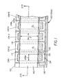
- FIG. 1 a schematic plan view of a top-emitting passive matrix OLED device 100 is shown which incorporates aspects of the present invention.
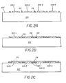
- FIGS. 2A-2E are schematic sectional views, taken along the section lines 2-2 in FIG. 1, and indicating a sequence of major process steps for making the OLED device 100.
- a plurality of laterally spaced lower electrodes 104-1, 104-2, 104-3, 104-4, 104-5 are formed on a substrate surface 103 of an electrically insulative substrate 102.
- Upper electrode busses 114, a bus connector 124, and a bus connector pad 126 can be formed at the same time on the substrate surface 103. Since the upper electrode busses 114 are single-level busses disposed in one and the same plane as the spaced lower electrodes, the busses 114 and the lower electrodes can be formed concurrently.
- the upper electrode busses 114 are formed so as to be laterally spaced from the lower electrodes 104-1 through 104-5. The result of this process step is depicted in FIG. 2A.
- the lower electrodes 104 can have a width dimension 104W in a range of 50-250 micrometer, and the upper electrode busses 114 can have a width dimension 114W in a range of 3-10 micrometer.
- Useful electrically insulative substrates 102 include glass substrates, quartz substrates, plastic substrates, ceramic substrates, and substrates having an electrically insulative surface layer provided over an otherwise electrically conductive substrate body.
- the lower electrodes 104-1 through 104-5, and the upper electrode busses 114, as well as the bus connector 124 and pad 126, are made of a metal, a metal alloy, or of a multilayer metal sandwich, and are formed at a thickness (not indicated in the drawings) selected to provide sufficiently high electrical conductivity, long-term physical and chemical stability, and adhesion to the substrate surface 103. Additionally, the selection of a metal has to be viewed in terms of a propensity to inject positive charge carriers (holes) into an organic electroluminescent organic electroluminescent (EL) medium structure. A metal having a work function ⁇ 4.0 eV is considered to have acceptable hole-injecting propensity.
- Hole-injecting propensity can be improved by providing a hole-injecting layer (not shown) over the lower electrodes.
- Particularly useful materials for forming a hole-injecting layer include conductive metal oxides such as, for example, indium-tin oxide (ITO), phthalocyanine compounds such as, for example, copper phthalocyanine, and plasma-deposited fluorocarbon materials (CFx).
- ITO indium-tin oxide
- phthalocyanine compounds such as, for example, copper phthalocyanine
- CFx plasma-deposited fluorocarbon materials
- particularly useful metals include silver, gold, platinum, iridium, tantalum, tungsten, molybdenum, nickel, and aluminum, or selected alloys, or sandwich structures of such metals.
- Various known methods can be chosen to provide the pattern of the lower electrodes, the upper electrode busses, the bus connector, and the bus connector pad.
- printing vapor deposition through a pattern mask
- vapor deposition of a pattern defined by a photoresist pattern in a so-called "lift-off'' process vapor deposition of a pattern defined by a photoresist pattern in a so-called "lift-off'' process
- patterning a uniformly deposited layer by selective etching via a photoresist etch mask are known methods.
- the thickness of the patterned metal features renders them optically opaque.
- Upper surfaces can be optically reflective, with a level of reflectivity determined by choice of metal or metals and by micro-topological aspects of the upper surface.
- electrical insulation 130 is formed between the lower electrodes 104 and the upper electrode busses 114 so that upper surfaces (not identified) of the busses are revealed.
- the electrical insulation can be an organic photoresist material, which has been patterned by a photolithographic process.
- the organic EL medium structure can be a multilayer structure which includes, in sequence, a hole-injecting layer, a hole-transporting layer, a light-emitting layer, an electron-transporting layer, and an electron-injecting layer.
- Such multilayer structures are well known in the art of designing and making OLED devices.
- the EL medium structure can include small molecule layers and polymer layers.
- top-emitting passive matrix OLED device 100 is designated to be a monochrome light-emitting device, one and the same organic EL medium structure is formed over all lower electrodes, electrical insulation, and upper electrode busses.
- the light-emitting layer of the multilayer structure is deposited selectively over selected lower electrodes. For example, a red light-emitting layer is formed over lower electrodes 104-1 and 104-4, and extends laterally over adjacent electrical insulation 130. A green light-emitting layer is formed over lower electrode 104-2, and a blue light-emitting layer is formed over lower electrode 104-3. These light-emitting layers overlap or abut over the insulation 130 or over the upper electrode busses 114. All other organic layers of the multilayer organic EL medium structure are commonly deposited over all lower electrodes, upper electrode busses, and electrical insulation.
- FIG. 2D depicts a step of selectively removing the organic EL medium structure from the upper electrode busses 114 and from portions of the electrical insulation 130, resulting in a width dimension 160W over the electrical insulation 130 upon removal of the EL medium.
- Selective removal of the organic EL medium structure occurs by selectively ablating the structure via radiation 150, which is selectively directed at zones or areas from which the EL medium structure is to be removed.
- Ablated material is indicated by arrows 160, which represent the directions of selective removal of the EL medium.
- this ablative process is carried out in a chamber (not shown) held at reduced pressure. It will be appreciated that the process of ablation includes resublimation of organic materials, which were originally deposited by a sublimation process.
- Selectively ablating portions of the organic EL medium structure can be accomplished by providing the radiation 150 in the form of a linear array of laser light beams directed towards the upper electrode busses, and by providing relative motion between the laser light beams and the substrate 102.
- Selectively ablating portions of the organic EL medium structure can also be achieved by providing a source of uniform radiation directed towards the organic EL medium structure, and by providing a mask between the source and the structure, with the mask having openings which are oriented with respect to the upper electrode busses 114.
- the radiation 150 is defined by openings in a mask.
- selectively ablating portions of the organic EL medium structure can be achieved by directing one or more laser light beams 150 towards the structure in registration with the upper electrode busses 114.
- the light transmissive upper electrode 140 can be formed of a thin metal film or of a layer of relatively transparent and electrically conductive metal oxides, or a combination of these materials.
- An electron-injecting interfacial layer for example a lithium fluoride (LiF) interfacial layer, may be formed as an uppermost layer of the EL medium structure, followed by a layer of aluminum (A1).
- layers of these materials comprise the light transmissive upper electrode 140, as described, for example in US-A-5,677,572.
- Other useful upper electrode material sets include, but are not limited to, those disclosed in Us-A-5,059,861 and US-A-5,059,862.
- transparent includes materials which pass sufficient light to permit the OLED device to operate effectively as a top-emitter.
- alternative thin films of transparent electrode material useful for the present invention include indium tin oxide (ITO) in combination with an electron-injecting layer or alloys of a low-work function material with other metals or alloys, for example, Li/Ag, LiF/Al/Ag, and alloys of magnesium with other metals (such as MgAg, MgAl, MgSn, MgIn, or MgZn, with or without an additional layer of Ag or any other highly conductive metals or alloys).
- ITO indium tin oxide
- LiF/Al/Ag LiF/Al/Ag
- magnesium such as MgAg, MgAl, MgSn, MgIn, or MgZn
- Optically transparent cathodes have been described in more detail in US-A-4,885,211; US-A-5,247,190; JP 3,234,963; US-A-5,703,436; US-A-5,608,287; US-A-5,837,391, US-A-5,677,572; US-A-5,776,622; US-A-5,776,623; US-A-5,714,838; US-A-5,969,474; US-A-5,739,545; US-A-5,981,306; US-A-6,137,223; US-A-6,140,763, US-A-6,172,459; EP 1 076 368; and US-A-6,278,236 and US-A-6,284,393.
- the electrical contact between the light transmissive common upper electrode 140 and each one of the metallic upper electrode busses 114 provides for improved power distribution within the upper electrode, thereby permitting the use of substantially light transmissive materials in forming the upper electrode. Stated differently, undesirable voltage drops along or across a light transmissive upper electrode can be substantially reduced or avoided by providing multiple electrical connections between such electrode and metallic, electrically conductive upper electrode busses 114.
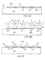
- FIGS. 3A-3C are schematic sectional views of an abbreviated sequence of process steps for making a modified top-emitting passive matrix OLED device 100 m, which differs from the device of FIG. 1 and FIGS. 2A-2E in that optically opaque electrical insulation 132 replaces the electrical insulation 130. Also, as shown in FIG. 3A, the insulation 132 extends initially over each of the upper electrode busses 114.
- the organic EL medium structure (“EL”) has been formed over the lower electrodes 104 and over an upper surface (not identified) of the electrical insulation 132.
- An intensity level of radiation 152 may be different from an intensity level of radiation 150 to meet the requirement of selectively removing a portion of the optically opaque electrical insulation 132, and to provide remaining insulation 133.
- the OLED illuminator device 200 is formed over a substrate surface 203 of a substrate 202. Electrical insulation 230, and common light transmissive upper electrode 240 correspond to electrical insulation 130, and to upper electrode 140, respectively, of the passive matrix OLED device 100 described above.
- one or more luminescent dopants are incorporated in a light-emitting layer or in a light-emitting zone of the EL medium structure, the dopant(s) selected to provide emission of white light from the device 200.
- the EL medium structure is shown in dotted outline in FIG. 4.
- a light-emitting portion px is defined here as the overlap area between a lower electrode 204 and the light transmissive upper electrode 240. It will be appreciated that light emission is provided concurrently by the EL medium structure formed over all lower electrodes since all lower electrodes are electrically connected in parallel.
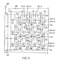
- FIG. 5 a non-limiting example is depicted of a partial view of a circuit diagram having a two-dimensional array of repeating units.
- This array is referred to as an active matrix array, and is useful for independently addressing and for driving pixels or subpixels of an OLED device.
- all of the following elements are included in each repeating unit, or are associated with each unit:
- the X-direction data driving circuit 380 receives data
- FIG. 5 Also identified in FIG. 5 are some anodes (lower electrodes of the present invention) of the diodes, namely 304-13 (lower electrode associated with a pixel 1 ;3), 304-23 (lower electrode associated with a pixel 2;3), and 304-33 (lower electrode associated with a pixel 3;3).
- Respectively corresponding connector contact pads 306-13, 306-23, and 306-33 constitute the electrical connections to associated anodes (lower electrodes of the present invention).
- the Y-direction scan driving circuit 390 sequentially provides a scan signal to each of the Y-direction scan lines Y1, Y2, Y3, ..., Ym at a voltage level sufficient to cause all TFTs for switching (TSs) along a scan line to be actuated into an "on" state.
- data are provided at the X-direction data lines X1, X2, X3, ..., Xn at data signal levels corresponding to data or image information to be displayed at the location of pixels or subpixels along an "actuated" scan line.
- FIGS. 7A-7F are schematic sectional views, taken along the section lines 7-7 of FIG. 6, and showing a non-limiting sequence of major process steps for making the top-emitting active matrix OLED display device of FIG. 6, in accordance with aspects of the present invention.
- Various alternative methods of patterning features, and alternative sequences of deposition, are known to those skilled in the art of photolithographic patterning and metal deposition. Such alternative methods and sequences can be used in the practice of the invention.
- bus lines and bus connections in conventional integrated circuits is well known.
- multiple levels of bus lines are disposed over a substrate surface and over electrically insulative layers formed over the substrate. Electrical connections between bus lines formed at multiple levels occurs through openings or vias created at particular locations in the insulative layer or layers.
- the connectors 305-12, 305-22 can be sized to provide sufficient electrical contact to respective connector contact pads 306-12, 306-22. Partial views of lower electrodes 304-13, 304-23, and 304-32 are also indicated in FIG. 6.
- Upper electrode busses 314 are depicted as extending laterally along or across an entire OLED device and are shown disposed in spaces between laterally spaced lower electrodes. Alternatively, a plurality of laterally spaced bus vias can replace the continuous upper electrode busses 314. Each one of the upper electrode busses 314 is in electrical contact with the common light transmissive upper electrode 340 to provide improved uniformity of current distribution or of power distribution in this common upper electrode.
- the first organic planarizing layer PLN1 can be an optically opaque photoresist layer which is formed, for example, by spin-coating a photoresist solution.
- the layer PLN1 is patterned by well known photolithography processes to create openings or trenches (not identified) in alignment with, and extending in depth to, the connector contact pads 306.
- Connectors 305-12 and 305-22 are then formed within these openings or trenches.
- the connectors can be formed of an elemental metal, a metal alloy, or of a sandwich structure of two or more metals such as, for example, a sandwich structure of molybdenum-aluminum-molybdenum.
- the connectors 305-12, 305-22 are in electrical contact with corresponding connector contact pads, such as the contact pad 306-12 identified in FIG. 7A.
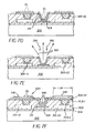
- FIG. 7C shows the process sequence upon deposition and patterning of lower electrodes 304-12, 304-22 over the connectors 305-12 and 305-22, respectively, and an upper electrode bus 314.
- the lower electrodes are in electrical contact with corresponding connectors 305-12, and 305-22
- the upper electrode bus 314 is in electrical contact with the connector 324.
- the active matrix OLED display device 300 usually includes multiple levels of bus lines.
- the uppermost level of bus lines, namely the upper electrode busses 314, are shown here in detail. These upper electrode busses 314 can be deposited and patterned concurrently with forming the lower electrodes 304.
- an organic EL medium structure has been deposited over the upper surfaces of the planarizing layer PLN1, the lower electrodes, and the upper electrode bus 314. If a top-emi7ting active matrix OLED display device is designated to be a multicolor device or a full-color device, neighbor EL medium structures providing different colors of light emission can abut or overlap within the lateral dimensions defined by the upper electrode busses 314.
- FIG. 7E shows a step of selectively removing the organic EL medium structure from the upper electrode busses 314. Selective removal occurs by selectively ablating the EL medium structure via radiation 356 which is selectively directed at the upper electrode busses. Ablated material is indicated by arrows 366 which represent the directions of selective removal of the EL medium.
- FIG. 7F depicts the completed top-emitting active matrix OLED display device 300 upon forming a common light transmissive upper electrode 340 over the organic EL medium structure and over the upper electrode busses 314.
- the common upper electrode 340 is in electrical contact with the upper electrode busses 314, thereby providing improved uniformity of current distribution or of power distribution in the common upper electrode.
- a light-emitting portion of a pixel or a subpixel px is indicated in FIG. 7F.
- a width dimension 304W of the lower electrodes can be in a range of 50-250 micrometer, while a width dimension 314W of upper electrode busses (or of bus vias) can be in a range of 3-10 micrometer.
- the process sequence of forming lower electrodes and upper electrode busses, depositing an organic EL medium structure over all features of a partial device, selectively removing the EL medium from the upper electrode busses, and forming a common light transmissive upper electrode in electrical contact with the busses permits a simplified method of making different classes of top-emitting OLED devices which have improved power distribution.
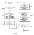
- FIG. 8 is a process flow chart showing a sequence of major process steps in obtaining a top-emitting OLED device, in accordance with aspects of the present invention.
- Step 520 includes providing a substrate having an electrically insulative substrate surface.
- Step 530 includes forming concurrently lower electrodes and upper electrode busses on the insulative substrate surface.
- Step 540 includes depositing an organic EL medium structure uniformly over the lower electrodes, the upper electrode busses, and other device features.
- Step 550 includes selectively removing the organic EL medium from the upper electrode busses.
- Step 560 includes depositing a common light transmissive upper electrode over the organic EL medium structure and over the upper electrode busses for obtaining a top-emitting OLED device, as indicated at 570.
- the process ends at 580.
- FIG. 9 depicts emission of white light 276W from an operative top-emitting OLED illuminator device 200, previously described with reference to FIG. 4.
- the organic EL medium structure commonly includes several sublayers which are formed, in sequence, starting with layer deposition over the lower electrodes and upper electrode busses, and over areas disposed between such elements on a surface.
- HIL Hole-Injecting Layer
- the hole-injecting material can serve to improve the film formation property of subsequent organic layers and to facilitate injection of holes into a hole-transporting layer.
- Suitable materials for use in the hole-injecting layer include, but are not limited to, porphyrinic compounds as described in US-A-4,720,432, plasma-deposited fluorocarbon polymers as described in US-A-6,208,075, and some aromatic amines, for example, m-MTDATA (4,4',4"-tris[(3-methylphenyl)phenylamino]-triphenylamine).
- Alternative hole-injecting materials reportedly useful in organic EL devices are described in EP 0 891 121 A1 and EP 1 029 909 A1.
- HTL Hole-Transporting Layer
- the hole-transporting layer contains at least one hole-transporting compound such as an aromatic tertiary amine, where the latter is understood to be a compound containing at least one trivalent nitrogen atom that is bonded only to carbon atoms, at least one of which is a member of an aromatic ring.
- the aromatic tertiary amine can be an arylamine, such as a monoarylamine, diarylamine, triarylamine, or a polymeric arylamine. Exemplary monomeric triarylamines are illustrated by Klupfel and others US-A-3,180,730.
- Other suitable triarylamines substituted with one or more vinyl radicals and/or comprising at least one active hydrogen containing group are disclosed by Brantley and others US-A-3,567,450 and US-A-3,658,520.
- a more preferred class of aromatic tertiary amines are those which include at least two aromatic tertiary amine moieties as described in US-A-4,720,432 and US-A-5,061,569.
- the hole-transporting layer can be formed of a single or a mixture of aromatic tertiary amine compounds.
- Illustrative of useful aromatic tertiary amines are the following:
- Another class of useful hole-transporting materials includes polycyclic aromatic compounds as described in EP 1 009 041. Tertiary aromatic amines with more than two amine groups may be used including oligomeric materials.
- polymeric hole-transporting materials can be used such as poly(N-vinylcarbazole) (PVK), polythiophenes, polypyrrole, polyaniline, and copolymers such as poly(3,4-ethylenedioxythiophene)/poly(4-styrenesulfonate) also called PEDOT/PSS.
- the dopant is usually chosen from highly fluorescent dyes, but phosphorescent compounds, for example, transition metal complexes as described in WO 98/55561, WO 00/18851, WO 00/57676, and WO 00/70655 are also useful. Dopants are typically coated as 0.01 to 10 % by weight into the host material. Polymeric materials such as polyfluorenes and polyvinylarylenes, for example, poly(p-phenylenevinylene), PPV, can also be used as the host material. In this case, small molecule dopants can be molecularly dispersed into the polymeric host, or the dopant could be added by copolymerizing a minor constituent into the host polymer.
- bandgap potential is defined as the energy difference between the highest occupied molecular orbital and the lowest unoccupied molecular orbital of the molecule.
- band gap of the dopant is smaller than that of the host material.
- phosphorescent emitters it is also important that the host triplet energy level of the host be high enough to enable energy transfer from host to dopant.
- Host and emitting molecules known to be of use include, but are not limited to, those disclosed in US-A-4,768,292; US-A-5,141,671; US-A-5,150,006; US-A-5,151,629; US-A-5,405,709; US-A-5,484,922; US-A-5,593,788; US-A-5,645,948; US-A-5,683,823; US-A-5,755,999; US-A-5,928,802; US-A-5,935,720; US-A-5,935,721; and US-A-6,020,078.
- ETL Electron-Transporting Layer
- Preferred thin film-forming materials for use in forming an electron-transporting layer of the organic EL medium structure of this invention are metal chelated oxinoid compounds, including chelates of oxine itself (also commonly referred to as 8-quinolinol or 8-hydroxyquinoline). Such compounds help to inject and transport electrons, exhibit high levels of performance, and are readily fabricated in the form of thin films. Exemplary oxinoid compounds were listed previously.
- White-emitting devices are described, for example, in EP 1 187 235, EP 1 182 244, US-A-5,683,823, US-A-5,503,910, US-A-5,405,709, and US-A-5,283,182.
- the organic materials mentioned above are suitably deposited through a vapor-phase method such as sublimation, but can be deposited from a fluid, for example, from a solvent with an optional binder to improve film formation. If the material is a polymer, solvent deposition is useful but other methods can be used, such as sputtering or thermal transfer from a donor sheet.
- the material to be deposited by sublimation can be vaporized from a sublimator "boat" often comprised of a tantalum material, for example, as described in US-A-6,237,529, or can be first coated onto a donor sheet and then sublimed in closer proximity to the substrate.
- the method of making OLED devices in accordance with this invention can employ various well known optical effects in order to enhance device performance if desired. This includes optimizing layer thicknesses to yield maximum light transmission, providing dielectric mirror structures, replacing reflective electrodes with light-absorbing electrodes, providing anti glare or anti-reflection coatings over the display, providing a polarizing medium over the display, or providing colored, neutral density, or color conversion filters over the display. Filters, polarizers, and anti-glare or anti-reflection coatings may be specifically provided over the cover or over an electrode protection layer beneath the cover.
- Another method of selectively removing organic EL material includes using an optical mask having openings which are aligned with respect to the upper electrode busses, and directing a flood exposure of laser light or light from another light source through the openings onto the device surface, so that organic EL material is ablated at the same time from all upper electrode busses.
- a further method of selectively removing organic EL material includes using one or more lasers configured to independently ablate organic EL material from upper electrode busses, and from other areas peripheral to light-emitting areas of an OLED device.
Landscapes
- Physics & Mathematics (AREA)
- Optics & Photonics (AREA)
- Engineering & Computer Science (AREA)
- Manufacturing & Machinery (AREA)
- Electroluminescent Light Sources (AREA)
- Devices For Indicating Variable Information By Combining Individual Elements (AREA)
Abstract
Description
- FIG. 1 is a schematic plan view of a top-emitting passive matrix OLED device having laterally spaced lower electrodes, and upper electrode busses in electrical contact with a light transmissive upper electrode;
- FIGS. 2A-2E show schematic sectional views of major process steps for making the OLED device of FIG. 1, in accordance with aspects of the present invention, in which
- FIG. 2A depicts providing laterally spaced lower electrodes and forming upper electrode busses;
- FIG. 2B shows electrical insulation formed between the lower electrodes and the upper electrode busses so that upper surfaces of the busses are revealed;
- FIG. 2C shows schematically in dotted outline an organic EL medium structure deposited over the lower electrodes, the insulation, and the upper electrode busses;
- FIG. 2D depicts schematically a step of selectively removing the organic EL medium structure from the upper electrode busses and from portions of the insulation; and
- FIG. 2E depicts the device of FIG. 1 upon forming a light transmissive upper electrode over the EL medium structure and in electrical contact with each of the upper electrode busses;
- FIGS. 3A-3C are schematic sectional views of major process steps for making a modified OLED device in which the electrical insulation is optically opaque, wherein
- FIG. 3A depicts the opaque electrical insulation extending initially over the upper electrode busses, and the organic EL medium structure deposited over the lower electrodes and over the electrical insulation;
- FIG. 3B shows schematically a step of selectively removing the organic EL medium structure and portions of the optically opaque electrical insulation so that surfaces of the upper electrode busses are revealed; and
- FIG. 3C depicts a modified top-emitting passive matrix OLED device upon forming a light transmissive upper electrode over the organic EL medium structure and in electrical contact with each of the upper electrode busses;
- FIG. 4 is a schematic plan view of a top-emitting OLED illuminator device having laterally spaced lower electrodes electrically connected in parallel, and upper electrode busses in electrical contact with a light transmissive upper electrode;
- FIG. 5 depicts a partial view of an example of a circuit diagram having a two-dimensional array of repeating units, and identifying some upper electrode busses shown as triple connections, lower electrodes, lower electrode contacts, and organic EL medium structures which are shown in the form of diodes;
- FIG. 6 is a schematic plan view of a portion of a top-emitting active matrix OLED display device in which individually addressable and optically opaque lower electrodes are connected to corresponding repeating units of the diagram of FIG. 5 and having a common light transmissive upper electrode in electrical contact with upper electrode busses;
- FIGS. 7A-7F show schematic sectional views of major process steps for making the top-emitting active matrix OLED display device of FIG. 6, in accordance with aspects of the present invention, in which
- FIG. 7A indicates lower electrode connectors connected to corresponding repeating circuit elements, a connector to an upper electrode bus, and a first organic planarizing layer in which the lower electrode connectors are formed;
- FIG. 7B shows a bus trench formed in the first organic planarizing layer for revealing the connector to an upper electrode bus, and showing lower electrode connectors containing a second organic planarizing layer;
- FIG. 7C depicts the process upon deposition of lower electrodes and upper electrode buss(es);
- FIG. 7D shows an organic electroluminescent (EL) medium structure formed over the lower electrodes, the upper electrode bus, and over portions of the first organic planarizing layer;
- FIG. 7E indicates schematically a step of selectively removing the EL medium structure over the upper electrode bus; and
- FIG. 7F depicts the device of FIG. 6 upon forming a light transmissive upper electrode over the EL medium structure and in electrical contact with each of the upper electrode busses;
- FIG. 8 is a process flow chart showing a sequence of major process steps in obtaining a top-emitting OLED device, in accordance with aspects of the present invention; and
- FIG. 9 depicts light emission from an operative top-emitting OLED illuminator device.
Claims (10)
- A method of making a top-emitting OLED device, comprising:a) providing over a substrate laterally spaced and optically opaque lower electrodes and upper electrode busses which are electrically insulated from the lower electrodes;b) depositing an organic EL medium structure over the lower electrodes and the upper electrode busses;c) selectively removing the organic EL medium structure over at least portions of the upper electrode busses to reveal at least upper surfaces of the upper electrode busses; andd) depositing a light transmissive upper electrode over the organic EL medium structure so that such upper electrode is in electrical contact with at least upper surfaces of the upper electrode busses.
- The method of claim I wherein element a) includes providing the lower electrodes and concurrently forming the upper electrode busses.
- The method of claim 1 further including making a top-emitting passive matrix OLED device, a top-emitting active-matrix OLED device, or a polymer OLED device (either active- or passive-matrix).
- The method of claim 1 further including providing electrically insulating material between each one of the upper electrode busses and adjacent lower electrodes.
- The method of claim 1 wherein element c) includes removing the organic EL medium structure by selectively ablating such EL medium structure.
- The method of claim 5 further including:i) providing a linear array of laser light beams directed towards the upper electrode busses; andii) providing relative motion between the laser light beams and the substrate having the upper electrode busses formed thereover.
- The method of claim 5 further including:i) providing a source of uniform radiation directed towards the organic EL medium structure; andii) providing a mask between the source and the structure and having openings oriented with respect to the upper electrode busses.
- The method of claim 5 further including directing one or more laser light beams towards the organic EL medium structure in registration with the upper electrode busses.
- The method of claim 3 further including providing an electrical connection to each one of the lower electrodes in making a top-emitting passive matrix OLED device or in making a top-emitting active matrix OLED display device.
- The method of claim 3 further including providing a common electrical connection to all of the lower electrodes in making a top-emitting OLED device.
Applications Claiming Priority (2)
| Application Number | Priority Date | Filing Date | Title |
|---|---|---|---|
| US10/462,360 US6995035B2 (en) | 2003-06-16 | 2003-06-16 | Method of making a top-emitting OLED device having improved power distribution |
| US462360 | 2003-06-16 |
Publications (3)
| Publication Number | Publication Date |
|---|---|
| EP1489671A2 true EP1489671A2 (en) | 2004-12-22 |
| EP1489671A3 EP1489671A3 (en) | 2011-12-14 |
| EP1489671B1 EP1489671B1 (en) | 2013-07-24 |
Family
ID=33418117
Family Applications (1)
| Application Number | Title | Priority Date | Filing Date |
|---|---|---|---|
| EP04076631.3A Expired - Lifetime EP1489671B1 (en) | 2003-06-16 | 2004-06-03 | Method of making a top-emitting OLED device having improved power distribution |
Country Status (6)
| Country | Link |
|---|---|
| US (1) | US6995035B2 (en) |
| EP (1) | EP1489671B1 (en) |
| JP (1) | JP4959119B2 (en) |
| KR (1) | KR20040111048A (en) |
| CN (1) | CN1574412A (en) |
| TW (1) | TW200503578A (en) |
Cited By (5)
| Publication number | Priority date | Publication date | Assignee | Title |
|---|---|---|---|---|
| WO2008139940A1 (en) * | 2007-04-27 | 2008-11-20 | Canon Kabushiki Kaisha | Light emitting apparatus and method of manufacturing the same |
| EP2333859A1 (en) | 2009-12-03 | 2011-06-15 | Novaled AG | A method for forming an organic light emitting diode |
| WO2011084207A1 (en) * | 2010-01-06 | 2011-07-14 | General Electric Company | Architecture for organic electronic devices |
| WO2014020853A1 (en) * | 2012-08-02 | 2014-02-06 | Sony Corporation | Display unit, method of manufacturing the same, and method of manufacturing electronic apparatus |
| EP3333924A1 (en) * | 2016-12-07 | 2018-06-13 | Samsung Display Co., Ltd. | Organic light emitting diode display and method of manufacturing the same |
Families Citing this family (117)
| Publication number | Priority date | Publication date | Assignee | Title |
|---|---|---|---|---|
| US7086917B2 (en) * | 2002-08-12 | 2006-08-08 | National Research Council Of Canada | Photoresist mask/smoothing layer ensuring the field homogeneity and better step-coverage in OLED displays |
| KR100786071B1 (en) * | 2003-12-08 | 2007-12-18 | 엘지전자 주식회사 | Organic EL element and its manufacturing method |
| US7452572B1 (en) * | 2004-03-11 | 2008-11-18 | The North Carolina State University | Procedure for preparing redox-active polymers on surfaces |
| JP2005327674A (en) * | 2004-05-17 | 2005-11-24 | Sharp Corp | Organic electroluminescent display element, display device having the same, and manufacturing method thereof |
| TWI240593B (en) * | 2004-10-15 | 2005-09-21 | Ind Tech Res Inst | Top-emitting organic light emitting diode (OLED) |
| JP2006179646A (en) * | 2004-12-22 | 2006-07-06 | Matsushita Electric Ind Co Ltd | Method for manufacturing solid-state imaging device |
| JP5136734B2 (en) * | 2004-12-28 | 2013-02-06 | エルジー エレクトロニクス インコーポレイティド | Organic electroluminescent device and manufacturing method thereof |
| JP4837295B2 (en) * | 2005-03-02 | 2011-12-14 | 株式会社沖データ | Semiconductor device, LED device, LED head, and image forming apparatus |
| US7341886B2 (en) * | 2005-03-03 | 2008-03-11 | Eastman Kodak Company | Apparatus and method for forming vias |
| US7384816B2 (en) * | 2005-03-03 | 2008-06-10 | Eastman Kodak Company | Apparatus and method for forming vias |
| US20060232195A1 (en) * | 2005-04-14 | 2006-10-19 | Eastman Kodak Company | OLED device having improved light output |
| US20060250084A1 (en) * | 2005-05-04 | 2006-11-09 | Eastman Kodak Company | OLED device with improved light output |
| KR101315086B1 (en) * | 2005-06-30 | 2013-10-08 | 코닌클리케 필립스 엔.브이. | Organic electronic device and method for manufacture thereof |
| JP4449857B2 (en) * | 2005-08-17 | 2010-04-14 | ソニー株式会社 | Manufacturing method of display device |
| US8062756B2 (en) * | 2005-08-26 | 2011-11-22 | The Regents oft the University of California | Stepwise growth of oligomeric redox-active molecules on a surface without the use of protecting groups |
| US7642109B2 (en) * | 2005-08-29 | 2010-01-05 | Eastman Kodak Company | Electrical connection in OLED devices |
| JP2007103098A (en) * | 2005-09-30 | 2007-04-19 | Seiko Epson Corp | Organic EL device manufacturing method, organic EL device, and electronic apparatus |
| US20070077349A1 (en) * | 2005-09-30 | 2007-04-05 | Eastman Kodak Company | Patterning OLED device electrodes and optical material |
| US7612496B2 (en) * | 2005-12-19 | 2009-11-03 | Eastman Kodak Company | OLED device having improved power distribution |
| JP4747868B2 (en) * | 2006-02-10 | 2011-08-17 | セイコーエプソン株式会社 | Manufacturing method of electro-optical device |
| US7638356B2 (en) * | 2006-07-11 | 2009-12-29 | The Trustees Of Princeton University | Controlled growth of larger heterojunction interface area for organic photosensitive devices |
| JP4438782B2 (en) | 2006-08-23 | 2010-03-24 | ソニー株式会社 | Display device manufacturing method and display device |
| US7985609B2 (en) * | 2006-11-17 | 2011-07-26 | Canon Kabushiki Kaisha | Light-emitting apparatus and production method thereof |
| US20080218068A1 (en) * | 2007-03-05 | 2008-09-11 | Cok Ronald S | Patterned inorganic led device |
| US7919352B2 (en) * | 2007-04-10 | 2011-04-05 | Global Oled Technology Llc | Electrical connection in OLED devices |
| JP4340982B2 (en) * | 2007-05-18 | 2009-10-07 | ソニー株式会社 | Manufacturing method of display device |
| WO2009007899A1 (en) * | 2007-07-11 | 2009-01-15 | Koninklijke Philips Electronics N.V. | Organic functional device and manufacturing method therefore |
| US7833074B2 (en) * | 2007-09-04 | 2010-11-16 | Global Oled Technology Llc | Method of making a top-emitting OLED device having improved power distribution |
| JP4600786B2 (en) * | 2007-12-18 | 2010-12-15 | ソニー株式会社 | Display device and manufacturing method thereof |
| US8692455B2 (en) | 2007-12-18 | 2014-04-08 | Sony Corporation | Display device and method for production thereof |
| JP5320755B2 (en) * | 2008-01-30 | 2013-10-23 | 住友化学株式会社 | ORGANIC ELECTROLUMINESCENCE ELEMENT AND ITS MANUFACTURING METHOD, SURFACE LIGHT SOURCE, LIGHTING DEVICE, AND DISPLAY DEVICE |
| JPWO2009133680A1 (en) * | 2008-04-28 | 2011-08-25 | パナソニック株式会社 | Display device and manufacturing method thereof |
| US20090278454A1 (en) * | 2008-05-12 | 2009-11-12 | Fedorovskaya Elena A | Oled display encapsulated with a filter |
| KR20100001642A (en) | 2008-06-27 | 2010-01-06 | 삼성전자주식회사 | Transparent display apparatus |
| US20100080929A1 (en) * | 2008-09-30 | 2010-04-01 | General Electric Company | System and method for applying a conformal barrier coating |
| US8033885B2 (en) * | 2008-09-30 | 2011-10-11 | General Electric Company | System and method for applying a conformal barrier coating with pretreating |
| WO2010046833A1 (en) * | 2008-10-21 | 2010-04-29 | Koninklijke Philips Electronics N.V. | Transparent oled device |
| JP5157825B2 (en) * | 2008-10-29 | 2013-03-06 | ソニー株式会社 | Manufacturing method of organic EL display |
| JP2011040277A (en) | 2009-08-11 | 2011-02-24 | Sony Corp | Display and its manufacturing method |
| JP5676175B2 (en) * | 2009-08-24 | 2015-02-25 | 三星ディスプレイ株式會社Samsung Display Co.,Ltd. | Thin film deposition apparatus and organic light emitting display device manufacturing method using the same |
| JP5328726B2 (en) * | 2009-08-25 | 2013-10-30 | 三星ディスプレイ株式會社 | Thin film deposition apparatus and organic light emitting display device manufacturing method using the same |
| JP5677785B2 (en) * | 2009-08-27 | 2015-02-25 | 三星ディスプレイ株式會社Samsung Display Co.,Ltd. | Thin film deposition apparatus and organic light emitting display device manufacturing method using the same |
| JP5611718B2 (en) * | 2009-08-27 | 2014-10-22 | 三星ディスプレイ株式會社Samsung Display Co.,Ltd. | Thin film deposition apparatus and organic light emitting display device manufacturing method using the same |
| US8876975B2 (en) | 2009-10-19 | 2014-11-04 | Samsung Display Co., Ltd. | Thin film deposition apparatus |
| KR101742114B1 (en) * | 2009-12-03 | 2017-05-31 | 노발레드 게엠베하 | A method for forming an electrical interconnection in an organic opto-electronic device, a method for producing an organic opto-electronic device, and an organic light emitting device |
| KR101084184B1 (en) | 2010-01-11 | 2011-11-17 | 삼성모바일디스플레이주식회사 | Thin film deposition apparatus |
| KR101174875B1 (en) | 2010-01-14 | 2012-08-17 | 삼성디스플레이 주식회사 | Apparatus for thin layer deposition, method for manufacturing of organic light emitting display apparatus using the same, and organic light emitting display apparatus manufactured by the method |
| KR101193186B1 (en) | 2010-02-01 | 2012-10-19 | 삼성디스플레이 주식회사 | Apparatus for thin layer deposition, method for manufacturing of organic light emitting display apparatus using the same, and organic light emitting display apparatus manufactured by the method |
| KR101156441B1 (en) * | 2010-03-11 | 2012-06-18 | 삼성모바일디스플레이주식회사 | Apparatus for thin layer deposition |
| KR101202348B1 (en) | 2010-04-06 | 2012-11-16 | 삼성디스플레이 주식회사 | Apparatus for thin layer deposition and method for manufacturing of organic light emitting display apparatus using the same |
| US8894458B2 (en) | 2010-04-28 | 2014-11-25 | Samsung Display Co., Ltd. | Thin film deposition apparatus, method of manufacturing organic light-emitting display device by using the apparatus, and organic light-emitting display device manufactured by using the method |
| KR101223723B1 (en) | 2010-07-07 | 2013-01-18 | 삼성디스플레이 주식회사 | Apparatus for thin layer deposition, method for manufacturing of organic light emitting display apparatus using the same, and organic light emitting display apparatus manufactured by the method |
| TWI425858B (en) | 2010-08-13 | 2014-02-01 | Au Optronics Corp | Organic light-emitting device, lighting device, and liquid crystal display |
| KR101678056B1 (en) | 2010-09-16 | 2016-11-22 | 삼성디스플레이 주식회사 | Apparatus for thin layer deposition, method for manufacturing of organic light emitting display apparatus using the same, and organic light emitting display apparatus manufactured by the method |
| TWI434598B (en) * | 2010-10-11 | 2014-04-11 | Au Optronics Corp | Organic light emitting diode module |
| KR101723506B1 (en) | 2010-10-22 | 2017-04-19 | 삼성디스플레이 주식회사 | Apparatus for organic layer deposition and method for manufacturing of organic light emitting display apparatus using the same |
| KR101738531B1 (en) | 2010-10-22 | 2017-05-23 | 삼성디스플레이 주식회사 | Method for manufacturing of organic light emitting display apparatus, and organic light emitting display apparatus manufactured by the method |
| KR20120045865A (en) | 2010-11-01 | 2012-05-09 | 삼성모바일디스플레이주식회사 | Apparatus for organic layer deposition |
| KR20120065789A (en) | 2010-12-13 | 2012-06-21 | 삼성모바일디스플레이주식회사 | Apparatus for organic layer deposition |
| KR101760897B1 (en) | 2011-01-12 | 2017-07-25 | 삼성디스플레이 주식회사 | Deposition source and apparatus for organic layer deposition having the same |
| US8432095B2 (en) * | 2011-05-11 | 2013-04-30 | Universal Display Corporation | Process for fabricating metal bus lines for OLED lighting panels |
| US8564192B2 (en) | 2011-05-11 | 2013-10-22 | Universal Display Corporation | Process for fabricating OLED lighting panels |
| KR101923174B1 (en) | 2011-05-11 | 2018-11-29 | 삼성디스플레이 주식회사 | ESC, apparatus for thin layer deposition therewith, and method for manufacturing of organic light emitting display apparatus using the same |
| KR101840654B1 (en) | 2011-05-25 | 2018-03-22 | 삼성디스플레이 주식회사 | Apparatus for organic layer deposition and method for manufacturing of organic light emitting display apparatus using the same |
| KR101852517B1 (en) | 2011-05-25 | 2018-04-27 | 삼성디스플레이 주식회사 | Apparatus for organic layer deposition and method for manufacturing of organic light emitting display apparatus using the same |
| KR101857249B1 (en) | 2011-05-27 | 2018-05-14 | 삼성디스플레이 주식회사 | Patterning slit sheet assembly, apparatus for organic layer deposition, method for manufacturing organic light emitting display apparatus and organic light emitting display apparatus |
| KR101826068B1 (en) | 2011-07-04 | 2018-02-07 | 삼성디스플레이 주식회사 | Apparatus for thin layer deposition |
| KR20130004830A (en) | 2011-07-04 | 2013-01-14 | 삼성디스플레이 주식회사 | Apparatus for thin layer deposition and method for manufacturing of organic light emitting display apparatus using the same |
| US9847372B2 (en) * | 2011-12-01 | 2017-12-19 | Micron Technology, Inc. | Solid state transducer devices with separately controlled regions, and associated systems and methods |
| KR20130069037A (en) | 2011-12-16 | 2013-06-26 | 삼성디스플레이 주식회사 | Apparatus for thin layer deposition, method for manufacturing of organic light emitting display apparatus using the same, and organic light emitting display apparatus |
| TWI461104B (en) * | 2011-12-20 | 2014-11-11 | 友達光電股份有限公司 | Organic electroluminescent element |
| JP5758314B2 (en) * | 2012-01-17 | 2015-08-05 | 株式会社東芝 | Organic electroluminescence device and lighting device |
| KR102013315B1 (en) | 2012-07-10 | 2019-08-23 | 삼성디스플레이 주식회사 | Method for manufacturing of organic light emitting display apparatus and organic light emitting display apparatus manufactured by the method |
| US9496524B2 (en) | 2012-07-10 | 2016-11-15 | Samsung Display Co., Ltd. | Organic layer deposition apparatus, method of manufacturing organic light-emitting display apparatus using the same, and organic light-emitting display apparatus manufactured using the method |
| KR101959974B1 (en) | 2012-07-10 | 2019-07-16 | 삼성디스플레이 주식회사 | Apparatus for organic layer deposition, method for manufacturing of organic light emitting display apparatus using the same, and organic light emitting display apparatus manufactured by the method |
| US9461277B2 (en) | 2012-07-10 | 2016-10-04 | Samsung Display Co., Ltd. | Organic light emitting display apparatus |
| KR101632298B1 (en) | 2012-07-16 | 2016-06-22 | 삼성디스플레이 주식회사 | Flat panel display device and manufacturing method thereof |
| KR102013318B1 (en) | 2012-09-20 | 2019-08-23 | 삼성디스플레이 주식회사 | Apparatus for thin layer deposition, method for manufacturing of organic light emitting display apparatus using the same, and organic light emitting display apparatus |
| KR20140050994A (en) | 2012-10-22 | 2014-04-30 | 삼성디스플레이 주식회사 | Organic light emitting display apparatus and method for manufacturing the same |
| WO2014080478A1 (en) * | 2012-11-21 | 2014-05-30 | パイオニア株式会社 | Light emitting device and method for producing light emitting device |
| KR102006878B1 (en) | 2012-12-27 | 2019-08-05 | 삼성디스플레이 주식회사 | Multi-function apparatus for testing and etching substrate and substrate processing apparatus |
| KR102079252B1 (en) * | 2013-05-21 | 2020-04-08 | 삼성디스플레이 주식회사 | Organinc light emitting display device and manufacturing method for the same |
| KR102079251B1 (en) | 2013-05-21 | 2020-04-08 | 삼성디스플레이 주식회사 | Organic light emitting display apparatus and method for manufacturing the same |
| US9450039B2 (en) | 2013-05-31 | 2016-09-20 | Samsung Display Co., Ltd. | Organic light emitting display apparatus and method of manufacturing the same |
| US9362345B2 (en) * | 2013-05-31 | 2016-06-07 | Samsung Display Co., Ltd. | Organic light emitting display apparatus and method of manufacturing the same |
| KR102108361B1 (en) | 2013-06-24 | 2020-05-11 | 삼성디스플레이 주식회사 | Apparatus for monitoring deposition rate, apparatus for organic layer deposition using the same, method for monitoring deposition rate, and method for manufacturing of organic light emitting display apparatus using the same |
| JP5804162B2 (en) | 2013-08-30 | 2015-11-04 | 大日本印刷株式会社 | Top emission type organic electroluminescence display device manufacturing method and top emission type organic electroluminescence display device forming lid |
| JP5790857B2 (en) | 2013-09-02 | 2015-10-07 | 大日本印刷株式会社 | Top emission type organic electroluminescence display device and manufacturing method thereof |
| JP5787015B2 (en) | 2013-09-02 | 2015-09-30 | 大日本印刷株式会社 | Top emission type organic electroluminescence display device and manufacturing method thereof |
| US9117785B2 (en) | 2013-11-22 | 2015-08-25 | Samsung Display Co., Ltd. | Display device and method of manufacturing the same |
| KR102162797B1 (en) | 2013-12-23 | 2020-10-08 | 삼성디스플레이 주식회사 | Method for manufacturing of organic light emitting display apparatus |
| JP2015125808A (en) | 2013-12-25 | 2015-07-06 | 三星ディスプレイ株式會社Samsung Display Co.,Ltd. | Display device |
| KR20150102180A (en) | 2014-02-27 | 2015-09-07 | 삼성디스플레이 주식회사 | Laser beam irradiation apparatus and manufacturing method of organic light emitting display apparatus using the same |
| JP2015207484A (en) | 2014-04-22 | 2015-11-19 | 三星ディスプレイ株式會社Samsung Display Co.,Ltd. | Display device, and manufacturing method of display device |
| KR102315824B1 (en) * | 2014-06-27 | 2021-10-20 | 엘지디스플레이 주식회사 | Organic light emitting display device and method of fabricating the same |
| KR102246294B1 (en) | 2014-08-04 | 2021-04-30 | 삼성디스플레이 주식회사 | organic light emitting display apparatus and manufacturing method thereof |
| KR102283459B1 (en) | 2015-01-02 | 2021-07-30 | 삼성디스플레이 주식회사 | Organic light-emitting display apparatus and manufacturing the same |
| KR102369301B1 (en) | 2015-02-13 | 2022-03-03 | 삼성디스플레이 주식회사 | Organic light emitting display apparatus and the fabrication method thereof |
| JP2016181332A (en) | 2015-03-23 | 2016-10-13 | 三星ディスプレイ株式會社Samsung Display Co.,Ltd. | Display device and manufacturing method of display device |
| CA3002752A1 (en) | 2015-10-26 | 2017-05-04 | Oti Lumionics Inc. | Method for patterning a coating on a surface and device including a patterned coating |
| KR102802931B1 (en) | 2016-12-02 | 2025-05-08 | 오티아이 루미오닉스 인크. | Device including a conductive coating disposed over emissive regions and method therefor |
| KR102563713B1 (en) | 2017-04-26 | 2023-08-07 | 오티아이 루미오닉스 인크. | Methods of patterning the coating of a surface and apparatus comprising the patterned coating |
| CN110832660B (en) | 2017-05-17 | 2023-07-28 | Oti照明公司 | Method of selectively depositing a conductive coating on a patterned coating and an apparatus comprising the conductive coating |
| US11751415B2 (en) | 2018-02-02 | 2023-09-05 | Oti Lumionics Inc. | Materials for forming a nucleation-inhibiting coating and devices incorporating same |
| US11489136B2 (en) | 2018-05-07 | 2022-11-01 | Oti Lumionics Inc. | Method for providing an auxiliary electrode and device including an auxiliary electrode |
| US12041842B2 (en) | 2018-07-02 | 2024-07-16 | Jdi Design And Development G.K. | Display panel patterning device |
| JP2020008741A (en) * | 2018-07-09 | 2020-01-16 | 株式会社Joled | Apparatus and method for manufacturing display panel |
| JP2022508040A (en) | 2018-11-23 | 2022-01-19 | オーティーアイ ルミオニクス インコーポレーテッド | Optoelectronic device containing light transmission region |
| KR20250160226A (en) | 2019-03-07 | 2025-11-11 | 오티아이 루미오닉스 인크. | Materials for forming a nucleation-inhibiting coating and devices incorporating same |
| JP7576337B2 (en) | 2019-05-08 | 2024-11-01 | オーティーアイ ルミオニクス インコーポレーテッド | Materials for forming nucleation-inhibiting coatings and devices incorporating same - Patents.com |
| US11832473B2 (en) | 2019-06-26 | 2023-11-28 | Oti Lumionics Inc. | Optoelectronic device including light transmissive regions, with light diffraction characteristics |
| KR20240134240A (en) | 2019-06-26 | 2024-09-06 | 오티아이 루미오닉스 인크. | Optoelectronic device including light transmissive regions with light diffraction characteristics |
| KR102818817B1 (en) | 2019-08-09 | 2025-06-11 | 오티아이 루미오닉스 인크. | Optoelectronic device including auxiliary electrode and partition |
| CN114631191B (en) * | 2019-10-10 | 2026-02-24 | 应用材料公司 | Method and apparatus for organic light emitting diode display structure |
| CN115552643B (en) | 2019-12-24 | 2025-08-19 | Oti照明公司 | Light emitting device including cover layer and method of manufacturing the same |
| US11985841B2 (en) | 2020-12-07 | 2024-05-14 | Oti Lumionics Inc. | Patterning a conductive deposited layer using a nucleation inhibiting coating and an underlying metallic coating |
| JP2022133759A (en) | 2021-03-02 | 2022-09-14 | 株式会社ジャパンディスプレイ | Display device |
Family Cites Families (22)
| Publication number | Priority date | Publication date | Assignee | Title |
|---|---|---|---|---|
| US43046A (en) * | 1864-06-07 | Improvement in roasting and desulphurizing ores and minerals | ||
| US158835A (en) * | 1875-01-19 | Improvement in mortising-tools | ||
| US11783A (en) * | 1854-10-10 | Railroad-chair machinery | ||
| JP3556990B2 (en) * | 1995-02-13 | 2004-08-25 | 出光興産株式会社 | Fine patterning method of organic electroluminescence device and device obtained therefrom |
| JP4124379B2 (en) * | 1995-08-08 | 2008-07-23 | パイオニア株式会社 | Organic electroluminescence device |
| US6433355B1 (en) * | 1996-06-05 | 2002-08-13 | International Business Machines Corporation | Non-degenerate wide bandgap semiconductors as injection layers and/or contact electrodes for organic electroluminescent devices |
| KR100282393B1 (en) * | 1998-06-17 | 2001-02-15 | 구자홍 | method for fabricating Organic Electroluminescent display Device |
| JP2000331783A (en) * | 1999-05-21 | 2000-11-30 | Tohoku Pioneer Corp | Organic EL display panel and manufacturing method thereof |
| US6444400B1 (en) * | 1999-08-23 | 2002-09-03 | Agfa-Gevaert | Method of making an electroconductive pattern on a support |
| US6294398B1 (en) * | 1999-11-23 | 2001-09-25 | The Trustees Of Princeton University | Method for patterning devices |
| JP2003517182A (en) * | 1999-12-17 | 2003-05-20 | オスラム オプト セミコンダクターズ ゲゼルシャフト ミット ベシュレンクテル ハフツング | Organic LED device encapsulation |
| JP4434411B2 (en) * | 2000-02-16 | 2010-03-17 | 出光興産株式会社 | Active drive type organic EL light emitting device and manufacturing method thereof |
| US6608449B2 (en) | 2000-05-08 | 2003-08-19 | Semiconductor Energy Laboratory Co., Ltd. | Luminescent apparatus and method of manufacturing the same |
| JP2002110345A (en) * | 2000-09-29 | 2002-04-12 | Toshiba Corp | Mask and method for manufacturing organic EL display element using the same |
| JP2002164167A (en) * | 2000-11-27 | 2002-06-07 | Denso Corp | Manufacturing method of organic EL device |
| US6763167B2 (en) * | 2000-12-20 | 2004-07-13 | Polaroid Corporation | Integral organic light emitting diode fiber optic printhead |
| US20020110673A1 (en) * | 2001-02-14 | 2002-08-15 | Ramin Heydarpour | Multilayered electrode/substrate structures and display devices incorporating the same |
| TWI257496B (en) | 2001-04-20 | 2006-07-01 | Toshiba Corp | Display device and method of manufacturing the same |
| JP2002318556A (en) * | 2001-04-20 | 2002-10-31 | Toshiba Corp | Active matrix type flat display device and manufacturing method thereof |
| US6569706B2 (en) * | 2001-09-19 | 2003-05-27 | Osram Opto Semiconductors Gmbh | Fabrication of organic light emitting diode using selective printing of conducting polymer layers |
| JP4058930B2 (en) * | 2001-10-09 | 2008-03-12 | セイコーエプソン株式会社 | ORGANIC ELECTROLUMINESCENT DEVICE, ITS MANUFACTURING METHOD, AND ELECTRONIC DEVICE |
| EP1343206B1 (en) * | 2002-03-07 | 2016-10-26 | Semiconductor Energy Laboratory Co., Ltd. | Light emitting apparatus, electronic apparatus, illuminating device and method of fabricating the light emitting apparatus |
-
2003
- 2003-06-16 US US10/462,360 patent/US6995035B2/en not_active Expired - Lifetime
-
2004
- 2004-05-03 TW TW093112427A patent/TW200503578A/en unknown
- 2004-06-03 EP EP04076631.3A patent/EP1489671B1/en not_active Expired - Lifetime
- 2004-06-15 KR KR1020040043882A patent/KR20040111048A/en not_active Withdrawn
- 2004-06-16 JP JP2004178541A patent/JP4959119B2/en not_active Expired - Lifetime
- 2004-06-16 CN CNA2004100495157A patent/CN1574412A/en active Pending
Cited By (11)
| Publication number | Priority date | Publication date | Assignee | Title |
|---|---|---|---|---|
| WO2008139940A1 (en) * | 2007-04-27 | 2008-11-20 | Canon Kabushiki Kaisha | Light emitting apparatus and method of manufacturing the same |
| EP2333859A1 (en) | 2009-12-03 | 2011-06-15 | Novaled AG | A method for forming an organic light emitting diode |
| WO2011084207A1 (en) * | 2010-01-06 | 2011-07-14 | General Electric Company | Architecture for organic electronic devices |
| WO2014020853A1 (en) * | 2012-08-02 | 2014-02-06 | Sony Corporation | Display unit, method of manufacturing the same, and method of manufacturing electronic apparatus |
| CN110233163A (en) * | 2012-08-02 | 2019-09-13 | 索尼公司 | Display device, its manufacturing method and the method for manufacturing electronic equipment |
| US11088355B2 (en) | 2012-08-02 | 2021-08-10 | Sony Corporation | Display unit with prevented current leakage, method of manufacturing the same, and method of manufacturing electronic apparatus |
| CN110233163B (en) * | 2012-08-02 | 2023-05-26 | 索尼公司 | Display device, its manufacturing method, and method of manufacturing electronic equipment |
| EP3333924A1 (en) * | 2016-12-07 | 2018-06-13 | Samsung Display Co., Ltd. | Organic light emitting diode display and method of manufacturing the same |
| CN108172597A (en) * | 2016-12-07 | 2018-06-15 | 三星显示有限公司 | Organic light emitting diode display and its manufacturing method |
| US10446613B2 (en) | 2016-12-07 | 2019-10-15 | Samsung Display Co., Ltd. | Method of manufacturing an organic light emitting diode display having an auxiliary member in contact with an upper surface of an auxiliary electrode |
| CN108172597B (en) * | 2016-12-07 | 2023-09-12 | 三星显示有限公司 | Organic light-emitting diode display and manufacturing method thereof |
Also Published As
| Publication number | Publication date |
|---|---|
| US20040253756A1 (en) | 2004-12-16 |
| KR20040111048A (en) | 2004-12-31 |
| CN1574412A (en) | 2005-02-02 |
| JP2005011810A (en) | 2005-01-13 |
| EP1489671A3 (en) | 2011-12-14 |
| US6995035B2 (en) | 2006-02-07 |
| EP1489671B1 (en) | 2013-07-24 |
| TW200503578A (en) | 2005-01-16 |
| JP4959119B2 (en) | 2012-06-20 |
Similar Documents
| Publication | Publication Date | Title |
|---|---|---|
| EP1489671B1 (en) | Method of making a top-emitting OLED device having improved power distribution | |
| US7166006B2 (en) | Method of manufacturing-OLED devices by deposition on curved substrates | |
| US6919681B2 (en) | Color OLED display with improved power efficiency | |
| US7250722B2 (en) | OLED device | |
| CN100483728C (en) | Organic electroluminescent device of electroluminescent unit with lamina | |
| EP1463117B1 (en) | Oled display with photosensor | |
| US6693296B1 (en) | OLED apparatus including a series of OLED devices | |
| US6771028B1 (en) | Drive circuitry for four-color organic light-emitting device | |
| US6670772B1 (en) | Organic light emitting diode display with surface plasmon outcoupling | |
| US7038373B2 (en) | Organic light emitting diode display | |
| KR101266369B1 (en) | Flat panel oled device having deformable substrate | |
| EP1403908B1 (en) | Oled lamp | |
| KR101182183B1 (en) | Flat panel oled device having deformable substrate | |
| US20060006792A1 (en) | Flat panel light emitting devices with two sided | |
| EP1385219A2 (en) | OLED displays with fiber-optic faceplates | |
| US6961032B2 (en) | Reducing the effects of shorts in pixels of an active matrix organic electroluminescent device | |
| US20040069985A1 (en) | Oled display with circular polarizer | |
| US7304428B2 (en) | Multilayered cathode structures having silver for OLED devices | |
| US20050170551A1 (en) | Manufacture of flat panel light emitting devices |
Legal Events
| Date | Code | Title | Description |
|---|---|---|---|
| PUAI | Public reference made under article 153(3) epc to a published international application that has entered the european phase |
Free format text: ORIGINAL CODE: 0009012 |
|
| AK | Designated contracting states |
Kind code of ref document: A2 Designated state(s): AT BE BG CH CY CZ DE DK EE ES FI FR GB GR HU IE IT LI LU MC NL PL PT RO SE SI SK TR |
|
| AX | Request for extension of the european patent |
Extension state: AL HR LT LV MK |
|
| RAP1 | Party data changed (applicant data changed or rights of an application transferred) |
Owner name: GLOBAL OLED TECHNOLOGY LLC |
|
| RAP1 | Party data changed (applicant data changed or rights of an application transferred) |
Owner name: GLOBAL OLED TECHNOLOGY LLC |
|
| PUAL | Search report despatched |
Free format text: ORIGINAL CODE: 0009013 |
|
| RIC1 | Information provided on ipc code assigned before grant |
Ipc: H01L 51/52 20060101AFI20111031BHEP Ipc: H01L 27/32 20060101ALI20111031BHEP Ipc: H01L 51/56 20060101ALN20111031BHEP |
|
| AK | Designated contracting states |
Kind code of ref document: A3 Designated state(s): AT BE BG CH CY CZ DE DK EE ES FI FR GB GR HU IE IT LI LU MC NL PL PT RO SE SI SK TR |
|
| AX | Request for extension of the european patent |
Extension state: AL HR LT LV MK |
|
| RIC1 | Information provided on ipc code assigned before grant |
Ipc: H01L 27/32 20060101ALI20111116BHEP Ipc: H01L 51/52 20060101AFI20111116BHEP Ipc: H01L 51/56 20060101ALN20111116BHEP |
|
| 17P | Request for examination filed |
Effective date: 20111205 |
|
| 17Q | First examination report despatched |
Effective date: 20120413 |
|
| AKX | Designation fees paid |
Designated state(s): DE FR GB NL |
|
| REG | Reference to a national code |
Ref country code: DE Ref legal event code: R079 Ref document number: 602004042803 Country of ref document: DE Free format text: PREVIOUS MAIN CLASS: H01L0051200000 Ipc: H01L0051520000 |
|
| GRAP | Despatch of communication of intention to grant a patent |
Free format text: ORIGINAL CODE: EPIDOSNIGR1 |
|
| RIC1 | Information provided on ipc code assigned before grant |
Ipc: H01L 51/56 20060101ALI20121129BHEP Ipc: H01L 27/32 20060101ALI20121129BHEP Ipc: H01L 51/52 20060101AFI20121129BHEP |
|
| GRAS | Grant fee paid |
Free format text: ORIGINAL CODE: EPIDOSNIGR3 |
|
| GRAA | (expected) grant |
Free format text: ORIGINAL CODE: 0009210 |
|
| AK | Designated contracting states |
Kind code of ref document: B1 Designated state(s): DE FR GB NL |
|
| REG | Reference to a national code |
Ref country code: GB Ref legal event code: FG4D |
|
| REG | Reference to a national code |
Ref country code: DE Ref legal event code: R096 Ref document number: 602004042803 Country of ref document: DE Effective date: 20130919 |
|
| REG | Reference to a national code |
Ref country code: NL Ref legal event code: VDEP Effective date: 20130724 |
|
| PG25 | Lapsed in a contracting state [announced via postgrant information from national office to epo] |
Ref country code: NL Free format text: LAPSE BECAUSE OF FAILURE TO SUBMIT A TRANSLATION OF THE DESCRIPTION OR TO PAY THE FEE WITHIN THE PRESCRIBED TIME-LIMIT Effective date: 20130724 |
|
| PLBE | No opposition filed within time limit |
Free format text: ORIGINAL CODE: 0009261 |
|
| STAA | Information on the status of an ep patent application or granted ep patent |
Free format text: STATUS: NO OPPOSITION FILED WITHIN TIME LIMIT |
|
| 26N | No opposition filed |
Effective date: 20140425 |
|
| REG | Reference to a national code |
Ref country code: DE Ref legal event code: R097 Ref document number: 602004042803 Country of ref document: DE Effective date: 20140425 |
|
| REG | Reference to a national code |
Ref country code: FR Ref legal event code: PLFP Year of fee payment: 13 |
|
| REG | Reference to a national code |
Ref country code: FR Ref legal event code: PLFP Year of fee payment: 14 |
|
| REG | Reference to a national code |
Ref country code: FR Ref legal event code: PLFP Year of fee payment: 15 |
|
| REG | Reference to a national code |
Ref country code: DE Ref legal event code: R079 Ref document number: 602004042803 Country of ref document: DE Free format text: PREVIOUS MAIN CLASS: H01L0051520000 Ipc: H10K0050800000 |
|
| PGFP | Annual fee paid to national office [announced via postgrant information from national office to epo] |
Ref country code: FR Payment date: 20230622 Year of fee payment: 20 Ref country code: DE Payment date: 20220914 Year of fee payment: 20 |
|
| PGFP | Annual fee paid to national office [announced via postgrant information from national office to epo] |
Ref country code: GB Payment date: 20230620 Year of fee payment: 20 |
|
| REG | Reference to a national code |
Ref country code: DE Ref legal event code: R071 Ref document number: 602004042803 Country of ref document: DE |
|
| REG | Reference to a national code |
Ref country code: GB Ref legal event code: PE20 Expiry date: 20240602 |
|
| PG25 | Lapsed in a contracting state [announced via postgrant information from national office to epo] |
Ref country code: GB Free format text: LAPSE BECAUSE OF EXPIRATION OF PROTECTION Effective date: 20240602 |
|
| PG25 | Lapsed in a contracting state [announced via postgrant information from national office to epo] |
Ref country code: GB Free format text: LAPSE BECAUSE OF EXPIRATION OF PROTECTION Effective date: 20240602 |