EP1489379A2 - Piezoelectric device, method of manufacturing it and electronic equipment comprising such a device - Google Patents
Piezoelectric device, method of manufacturing it and electronic equipment comprising such a device Download PDFInfo
- Publication number
- EP1489379A2 EP1489379A2 EP20040014053 EP04014053A EP1489379A2 EP 1489379 A2 EP1489379 A2 EP 1489379A2 EP 20040014053 EP20040014053 EP 20040014053 EP 04014053 A EP04014053 A EP 04014053A EP 1489379 A2 EP1489379 A2 EP 1489379A2
- Authority
- EP
- European Patent Office
- Prior art keywords
- support substrate
- resonator element
- lead wire
- lead wires
- piezoelectric device
- Prior art date
- Legal status (The legal status is an assumption and is not a legal conclusion. Google has not performed a legal analysis and makes no representation as to the accuracy of the status listed.)
- Granted
Links
Images


Classifications
-
- G—PHYSICS
- G01—MEASURING; TESTING
- G01C—MEASURING DISTANCES, LEVELS OR BEARINGS; SURVEYING; NAVIGATION; GYROSCOPIC INSTRUMENTS; PHOTOGRAMMETRY OR VIDEOGRAMMETRY
- G01C19/00—Gyroscopes; Turn-sensitive devices using vibrating masses; Turn-sensitive devices without moving masses; Measuring angular rate using gyroscopic effects
- G01C19/56—Turn-sensitive devices using vibrating masses, e.g. vibratory angular rate sensors based on Coriolis forces
-
- H—ELECTRICITY
- H10—SEMICONDUCTOR DEVICES; ELECTRIC SOLID-STATE DEVICES NOT OTHERWISE PROVIDED FOR
- H10N—ELECTRIC SOLID-STATE DEVICES NOT OTHERWISE PROVIDED FOR
- H10N30/00—Piezoelectric or electrostrictive devices
- H10N30/80—Constructional details
-
- Y—GENERAL TAGGING OF NEW TECHNOLOGICAL DEVELOPMENTS; GENERAL TAGGING OF CROSS-SECTIONAL TECHNOLOGIES SPANNING OVER SEVERAL SECTIONS OF THE IPC; TECHNICAL SUBJECTS COVERED BY FORMER USPC CROSS-REFERENCE ART COLLECTIONS [XRACs] AND DIGESTS
- Y10—TECHNICAL SUBJECTS COVERED BY FORMER USPC
- Y10T—TECHNICAL SUBJECTS COVERED BY FORMER US CLASSIFICATION
- Y10T29/00—Metal working
- Y10T29/42—Piezoelectric device making
-
- Y—GENERAL TAGGING OF NEW TECHNOLOGICAL DEVELOPMENTS; GENERAL TAGGING OF CROSS-SECTIONAL TECHNOLOGIES SPANNING OVER SEVERAL SECTIONS OF THE IPC; TECHNICAL SUBJECTS COVERED BY FORMER USPC CROSS-REFERENCE ART COLLECTIONS [XRACs] AND DIGESTS
- Y10—TECHNICAL SUBJECTS COVERED BY FORMER USPC
- Y10T—TECHNICAL SUBJECTS COVERED BY FORMER US CLASSIFICATION
- Y10T29/00—Metal working
- Y10T29/43—Electric condenser making
- Y10T29/435—Solid dielectric type
-
- Y—GENERAL TAGGING OF NEW TECHNOLOGICAL DEVELOPMENTS; GENERAL TAGGING OF CROSS-SECTIONAL TECHNOLOGIES SPANNING OVER SEVERAL SECTIONS OF THE IPC; TECHNICAL SUBJECTS COVERED BY FORMER USPC CROSS-REFERENCE ART COLLECTIONS [XRACs] AND DIGESTS
- Y10—TECHNICAL SUBJECTS COVERED BY FORMER USPC
- Y10T—TECHNICAL SUBJECTS COVERED BY FORMER US CLASSIFICATION
- Y10T29/00—Metal working
- Y10T29/49—Method of mechanical manufacture
- Y10T29/49002—Electrical device making
- Y10T29/49005—Acoustic transducer
-
- Y—GENERAL TAGGING OF NEW TECHNOLOGICAL DEVELOPMENTS; GENERAL TAGGING OF CROSS-SECTIONAL TECHNOLOGIES SPANNING OVER SEVERAL SECTIONS OF THE IPC; TECHNICAL SUBJECTS COVERED BY FORMER USPC CROSS-REFERENCE ART COLLECTIONS [XRACs] AND DIGESTS
- Y10—TECHNICAL SUBJECTS COVERED BY FORMER USPC
- Y10T—TECHNICAL SUBJECTS COVERED BY FORMER US CLASSIFICATION
- Y10T29/00—Metal working
- Y10T29/49—Method of mechanical manufacture
- Y10T29/49002—Electrical device making
- Y10T29/49117—Conductor or circuit manufacturing
- Y10T29/49169—Assembling electrical component directly to terminal or elongated conductor
-
- Y—GENERAL TAGGING OF NEW TECHNOLOGICAL DEVELOPMENTS; GENERAL TAGGING OF CROSS-SECTIONAL TECHNOLOGIES SPANNING OVER SEVERAL SECTIONS OF THE IPC; TECHNICAL SUBJECTS COVERED BY FORMER USPC CROSS-REFERENCE ART COLLECTIONS [XRACs] AND DIGESTS
- Y10—TECHNICAL SUBJECTS COVERED BY FORMER USPC
- Y10T—TECHNICAL SUBJECTS COVERED BY FORMER US CLASSIFICATION
- Y10T29/00—Metal working
- Y10T29/49—Method of mechanical manufacture
- Y10T29/49002—Electrical device making
- Y10T29/49117—Conductor or circuit manufacturing
- Y10T29/49174—Assembling terminal to elongated conductor
Definitions
- This invention relates to a piezoelectric device using a resonator element such as quartz, a manufacturing method of a piezoelectric device, and electronic equipment on which a piezoelectric device is mounted.
- FIG. 11 A configuration of a conventional piezoelectric device is shown in FIG. 11 and described below.
- a piezoelectric resonator element 110 is connected to and held by the other ends of the lead wires 112A and 112B, respectively.
- the support substrate 113 is configured such that the lead wires 112A and 112B are affixed to a surface which is remote from the surface that faces the package 114.
- Au splash a splash of deposited gold particles
- Another object of this invention is to prevent Au splash from depositing on the lead wires, by receiving the Au splash on the support substrate provided on an upper surface of the lead wires, thereby preventing a short circuit between the lead wires.
- the lead wire is affixed to a lower surface of the support substrate, that is, a surface opposite to the package, it is possible to make the lead wire to adhere closely to the base substrate, thus dispensing with lead forming processing. Namely, it is possible to enhance ease of processing and to provide a piezoelectric device of low cost.
- receiving an Au splash on the support substrate located on the upper surface of the lead wire is made possible, so that a short circuit between lead wires may be prevented by keeping the Au splash from deposing on the lead wire.
- a gyro sensor using a quartz resonator element will be used and described as an example.
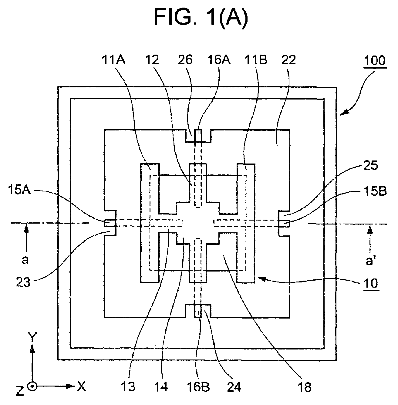
- FIG. 1 is a diagram illustrating a configuration of a gyro sensor as an example of a piezoelectric device.
- FIG. 1 (A) is a plan view
- FIG. 1 (B) is a front view showing a section along a - a'.
- a gyro sensor 100 is mounted thereon and used.
- the gyro sensor 100 comprises a gyro resonator element 10, which is a piezoelectric resonator element; lead wires 15A, 15B, 16A and 16B which are a support mechanism to support the resonator element 10; a support substrate 22; a package 20 made of, e.g., ceramic, accommodating the resonator element 10 supported by way of the lead wires and the support substrate 22 therein; and a cover 19 for the package 20.
- FIG. 2 shows a motion of a drive arm.
- FIG. 3 shows a relationship between the motion of the drive arm and the Coriolis force.
- FIG. 4 indicates the motion of a detecting arm.
- the resonator element 10 used in the gyro sensor 100 includes a first drive arm 11 A and a second drive arm 11B which constitute a drive unit, a detection arm 12 which is a detection unit, an arm support part 13, and a support plate 14 which is a support part.
- the first and the second drive arm 11A and 11B are members in a plate shape having a prescribed length which respectively extend in an illustrated direction Y, that is, mutually in parallel.
- X, Y and Z in the following text refer to axes of a Cartesian coordinate system as defined in the Figures.
- the first and the second drive arm 11A and 11B are influenced, during vibration along the direction X, by the Coriolis force corresponding to the magnitude of the rotary angular velocity of a rotation around an axis that extends in direction Z, which is one variation of the posture of the object.
- the drive arm 11A vibrates according to a bending motion with its center as a fulcrum; to be more specific, the drive arm 11A is alternately deformed to a convex shape and a concave shape while vibrating, namely, the opposite longitudinal ends of the drive arm are displaced along the X axis relative to the longitudinal center of the drive arm 11 A.
- the drive arm 11B vibrates correspondingly such that its shape becomes axisymmetrical to that of the drive arm 11A.
- FIG. 3 shows the relationship between the deformation of the drive arm and the Coriolis force.
- the first drive arm 11A deforms from the shape illustrated by a broken line to the shape illustrated by a solid line
- the second drive arm 11B also deforms from the shape illustrated by a broken line to the shape illustrated by a solid line, they are subjected to the Coriolis force along the arrows 19A and 19B, respectively, in response to a clockwise rotation in the plane of the drawing.
- the Coriolis force acts in directions opposite to the arrows 19A and 19B in response to the same clockwise rotation.
- the detection arm 12 is, like the first drive arm 11A and the second drive arm 11B, a plate member having a prescribed length extending along the Y direction. Namely, the first drive arm 11A, the second drive arm 11B, and the detection arm 12 are mutually parallel. To detect the Coriolis force acting on the first and the second drive arm 11A and 11B, the detection arm 12 responds to the Coriolis force conveyed from the first and the second drive arm 11A and 11B through the arm support 13 and vibrates corresponding to the magnitude of the Coriolis force.
- the detection arm 12 performs a bending motion of deforming into shape substantially like the letter S and the reverse of the letter S, like the bending motion of the first and the second drive arm 11A and 11B shown in FIG. 3(A) - 3(C).
- the magnitude of the Coriolis force is known, whereby the magnitude of the rotary angular velocity applied to the object is discerned.
- one end of the arm support part 13 is connected to the center of the first drive arm 11A, the other end is connected to the center of the second drive arm 11B, and the center of the arm support part 13 is connected to the detection arm 12 such that it corresponds to the center of the detection arm 12.
- the support plate 14 is a plate shape member having a prescribed area including the connection point of the arm support part 13 and the detection arm 12.
- the lead wires 15A and 15B extending in the X direction and the lead wires 16A and 16B extending in the Y direction are band or stripe like members having the same or a different shape.
- a first end portion of each of the lead wires 15A, 15B, 16A and 16B is, as shown in FIG. 1 (B), connected to one side (the lower side in the figure) of the support plate 14 of the resonator element 10, and the respective second end portions are connected to the package 20.
- the lead wires 15A, 15B, 16A and 16B are affixed by a support substrate 22 provided such that those second end portions are sandwiched between the support substrate 22 and the package 20.
- the lead wires 15A, 15B, 16A and 16B are formed such that the gyro resonator element 10 may not be in touch with the support substrate 22 and the package 20.
- both end portions of each of the lead wires 15A and 15B are connected by a connecting portion which is inclined so as to extend in the Z direction as well as in the X direction in a way that the distance between the first end portions of the two lead wires in the X direction is smaller than that between the second end portions, and the first end portions are positioned on a first plane (plane of resonator element 10) while the second end portions are positioned on a second plane (bottom surface 21 of the package 20) spaced apart in the Z direction from the first plane.
- the support substrate 22 comprises, for example, as shown in the enlarged sectional view in FIG. 5, a stainless steel plate 30 having an insulating layer 31 of a polyimide resin or the like formed on the surface side thereof that faces the bottom surface 21 of the package 20.
- the lead wires 15A, 15B, 16A and 16B are affixed to the insulating layer 31 and sandwiched between the latter and the bottom surface 21.
- a central opening part 18 (FIG. 1(A)) is formed in the support substrate 22 to allow the connecting portions of the lead wires to pass through. Further, cut-outs 23, 24, 25, 26 are provided at the outer peripheral portions of the support substrate 22 in the vicinity of the outermost end of the second end portion of each of the lead wires.
- the cut-outs 23, 24, 25, and 26 may have a semicircular shape, a substantially rectangular shape with rounded corners or the like, or any other shape as long as they does not hinder connecting the second end portion of a respective lead wire to the package 20.
- the lead wires are affixed to a lower surface of the support substrate 22, that is, the surface that faces the package 20, it is possible to affix the lead wires to the package 20 without subjecting the lead wires to the lead forming as defined above.
- the Au splash is prevented from depositing on the lead wires, thus making it possible to prevent a short circuits between lead wires.
- FIG. 7 presents a diagram showing connections of both end portions of the lead wire 15A as being representative for all lead wires 15A, 15B, 16A, 16B.
- the lead wires affixed to the support substrate 22 are formed into a prescribed shape at the cut-out of the support substrate 22.
- connection among the lead wires and the gyro resonator element 10 are made.
- the lead wires, one end portion of which being supported on the package 20, have the gyro resonator element 10 placed on the other end portions, and after coating a conductive bond 33, they are dried and connected to support electrodes 27 of the gyro resonator element 10.
- the formed lead wires are affixed to the package 20.
- Au bumps 32 are placed on the package 20, and the lead wires are placed on the Au bumps 32, respectively.
- a heating tool 29 or the like is inserted into each cut-out (23-26), and the lead wires, the Au bumps 32, and the package are affixed by applying pressure while heating them.
- the processing sequence may well be the reverse, so that after first connecting the lead wires to the package, the gyro resonator element may be affixed to the lead wires.
- heating efficiency may be enhanced. Also, stable affixing work can be performed.
- FIG. 6(A) is a plan view and FIG. 6(B) is a front sectional view along line a-a' in FIG. 6(A) of a gyro sensor as an example of the piezo-electric device according to the second embodiment.
- the gyro sensor configuration in this embodiment is the same as that described above for the first embodiment. Also, the configuration of the resonator element is the same as that in the first embodiment.
- the lead wires 40A and 40B extending in the X direction and 41A and 41B extending in the Y direction correspond to the lead wires 15A, 15B, 16A and 16B, respectively, of the first embodiment. They are band or stripe like members having either the same shape or different shapes. A first end portion of each of these lead wires is, as shown in FIG. 6(B), connected to one side of the support plate 14, and the second end portions are connected to the package 46.
- the lead wires 40A, 40B, 41A and 41B are affixed by a support substrate 42 provided so as to hold the lead wires on the package 46.
- the lead wires 40A, 40B, 41A and 41B are formed such that the gyro resonator element 10 may not be in touch with the package 46 but be positioned on a concave part 45 provided in the bottom surface 48 of the package 46.
- both end portions of each of the lead wires 40A and 40B are connected by a connecting portion which is inclined so as to extend in the Z direction as well as in the X direction in a way that the distance between the first end portions of the two lead wires in the X direction is smaller than that between the second end portions and the first end portions are positioned on a first plane (plane of resonator element 10) while the second end portions are positioned on a second plane (bottom surface 48 of the package 46) spaced apart in the Z direction from the first plane.
- the support substrate 41 comprises, for example, a stainless steel plate having an insulating layer of a polyimide resin or the like formed on the surface side that faces the bottom surface 48 of the package 46.
- the lead wires 40A, 40B, 41A and 41B are affixed to the insulating layer and sandwiched between the latter and the bottom surface 48 of the package 46.
- a central opening 43 (FIG. 6(A)) is formed in the support substrate 42 for forming the lead wires.
- cut-outs 23, 24, 25, and 26 are provided in the same way as has been described for the first embodiment. The description regarding the first embodiment of possible shapes for the these cut-outs applies to this second embodiment in the same way.
- the lead wires are affixed to a lower surface of the support substrate 42, namely, the surface that faces the package 46, it is possible to closely adhere the lead wires to the package 46 without subjecting the lead wires to lead forming.
- FIG. 9 An alternative is shown in a front sectional view of FIG. 9.
- This alternative configuration uses a shape without bending the lead wires (one lead wire 35 being shown as representative of four lead wires corresponding to those mentioned above), namely, a first end portion of the lead wires is affixed to the gyro resonator element 10 and the second end portion of the lead wires is affixed to the surface side of the support substrate 36 that faces the package 37 and extends at the same level as the gyro resonator element 10 such that the lead wires are plane.
- FIG. 10 is a front sectional view showing a configuration of a piezoelectric oscillator of this invention.
- the piezoelectric oscillator 50 comprises a piezoelectric resonator element 60, a plurality of lead wires 55A and 55B (in this example, two wires of 55A and 55B will be described) which are a support mechanism to hold the piezoelectric resonator element 60, a package 58, for example, a ceramic package for the piezoelectric resonator element 60 to be placed in through the lead wires 55A and 55B, a support substrate 56 to support the lead wires 55A and 55B, a circuit element 57 having a function to oscillate the piezoelectric resonator element 60, and a cover 59 for housing members such as the piezoelectric resonator element 60 in the package 58.
- lead wires 55A and 55B in this example, two wires of 55A and 55B will be described
- the lead wires 55A and 55B are affixed by a support substrate 56 provided in a positional relationship of holding the lead wires 55A and 55B onto the package 58.
- the lead wires 55A and 55B are formed such that the piezoelectric resonator element 60 may not be in touch with the package 58 or the circuit element 57 and the like but be positioned inside the package 58.
- the lead wires 55A and 55B are shaped in the same way as has been described in detail for the lead wires 15A and 15B in the context of the first embodiment.
- the lead wires are affixed to the lower surface of the support substrate 56, namely, the surface facing the package 58, it is possible to adhere the lead wires closely to the package 58 without subjecting the lead wires to lead forming.
- the piezo-electric resonator element or the piezoelectric oscillator of this invention may be used in, for example, electronic equipment such as mobile phones, video cameras, digital cameras, and personal computers, for a control reference signal, a reference signal of clock function, or a sensor and the like.
Landscapes
- Physics & Mathematics (AREA)
- Engineering & Computer Science (AREA)
- General Physics & Mathematics (AREA)
- Radar, Positioning & Navigation (AREA)
- Remote Sensing (AREA)
- Gyroscopes (AREA)
- Piezo-Electric Or Mechanical Vibrators, Or Delay Or Filter Circuits (AREA)
Abstract
Description
- This invention relates to a piezoelectric device using a resonator element such as quartz, a manufacturing method of a piezoelectric device, and electronic equipment on which a piezoelectric device is mounted.
- A configuration of a conventional piezoelectric device is shown in FIG. 11 and described below.
- In the configuration of the conventional piezoelectric device, to a
package 114, which is a substrate member,lead wires support substrate 113 are connected, and apiezoelectric resonator element 110 is connected to and held by the other ends of thelead wires support substrate 113 is configured such that thelead wires package 114. - According to the above-mentioned configuration, so as to secure close adhesion of the lead wires with the
package 114 at a junction thereof, it was necessary to have them bent in accordance with the thickness of the support substrate present in between the lead wires and the package (hereinafter referred to as "lead forming"). - Because of the lead wires being exposed on an upper surface, for example, due to a splash of deposited gold particles (hereinafter referred to as "Au splash") which occurs when tuning a vibration frequency of the resonator element, there was a problem of generating a short circuit between the lead wires.
- It is an object of the invention to enable the lead wires to adhere closely to the substrate without said so-called "lead forming" by affixing the lead wires to a lower surface of the support substrate, that is, a surface facing the package, and thus to dispense with lead forming processing. Another object of this invention is to prevent Au splash from depositing on the lead wires, by receiving the Au splash on the support substrate provided on an upper surface of the lead wires, thereby preventing a short circuit between the lead wires.
- These objects are achieved by a piezoelectric device as claimed in
claim 1 and a method of manufacturing it as claimed inclaim 10. Preferred embodiments of this invention are subject-matter of the dependent claims. - According to the piezoelectric resonator element of this invention, since the lead wire is affixed to a lower surface of the support substrate, that is, a surface opposite to the package, it is possible to make the lead wire to adhere closely to the base substrate, thus dispensing with lead forming processing. Namely, it is possible to enhance ease of processing and to provide a piezoelectric device of low cost.
- Also, receiving an Au splash on the support substrate located on the upper surface of the lead wire is made possible, so that a short circuit between lead wires may be prevented by keeping the Au splash from deposing on the lead wire.
- Preferred embodiments of this invention and the achieved advantages will be described in detail below with reference to the drawings, in which:
- FIG. 1
- is an explanatory diagram showing a configuration of a gyro sensor as an example of a piezoelectric device, FIG. 1(A) being a plan view, and FIG. 1(B) being a front view showing a section along the line a-a' in Fig. 1(A);
- FIG. 2(A) to (C)
- are diagrams showing a motion of a drive arm;
- FIG. 3
- is a diagram showing a relationship between the motion of the drive arm and the Coriolis force;
- FIG. 4(A)
- to (C) are diagrams showing a motion of a detection arm;
- FIG. 5
- is a sectional view of a structure of a
support substrate 22; - FIG. 6
- is an explanatory diagram showing a configuration of the gyro sensor as an example of the piezoelectric device, FIG. 6(A) being a plan view, and FIG. 6(B) being a front view showing a section along the line a-a' in Fig. 6a;
- FIG. 7(A)
- and (B) show diagrams illustrating connection methods of both ends of a lead wire;
- FIG. 8
- shows a diagram illustrating application examples of a cut-out of the support substrate;
- FIG. 9
- is a front sectional view showing an application example of this invention;
- FIG. 10
- is a front sectional view showing a configuration of the piezoelectric device of this invention; and
- FIG. 11
- is a diagram showing a configuration of a conventional piezoelectric device.
- In this embodiment, a gyro sensor using a quartz resonator element will be used and described as an example.
- Gyro Sensor Configuration
- FIG. 1 is a diagram illustrating a configuration of a gyro sensor as an example of a piezoelectric device. FIG. 1 (A) is a plan view, and FIG. 1 (B) is a front view showing a section along a - a'.
- According to FIG. 1, to detect a posture of an object such as an electronic equipment and a vehicle, a
gyro sensor 100 is mounted thereon and used. Thegyro sensor 100 comprises agyro resonator element 10, which is a piezoelectric resonator element;lead wires resonator element 10; asupport substrate 22; apackage 20 made of, e.g., ceramic, accommodating theresonator element 10 supported by way of the lead wires and thesupport substrate 22 therein; and acover 19 for thepackage 20. - Referring to FIG. 1(A) and FIG. 1 (B), a first embodiment will be described below using FIG. 2, FIG. 3, and FIG. 4. FIG. 2 shows a motion of a drive arm. FIG. 3 shows a relationship between the motion of the drive arm and the Coriolis force. FIG. 4 indicates the motion of a detecting arm.
- To operate in three modes known as drive mode, detection mode, and spurious mode, the
resonator element 10 used in thegyro sensor 100 includes afirst drive arm 11 A and asecond drive arm 11B which constitute a drive unit, adetection arm 12 which is a detection unit, anarm support part 13, and asupport plate 14 which is a support part. - As shown in FIG. 1(A), the first and the
second drive arm second drive arm - The
drive arm 11A, as shown in FIG. 2(A)-2(C), vibrates according to a bending motion with its center as a fulcrum; to be more specific, thedrive arm 11A is alternately deformed to a convex shape and a concave shape while vibrating, namely, the opposite longitudinal ends of the drive arm are displaced along the X axis relative to the longitudinal center of thedrive arm 11 A. Thedrive arm 11B vibrates correspondingly such that its shape becomes axisymmetrical to that of thedrive arm 11A. - FIG. 3 shows the relationship between the deformation of the drive arm and the Coriolis force. As shown in FIG. 3, while the
first drive arm 11A deforms from the shape illustrated by a broken line to the shape illustrated by a solid line and thesecond drive arm 11B also deforms from the shape illustrated by a broken line to the shape illustrated by a solid line, they are subjected to the Coriolis force along thearrows first drive arm 11A deforms from the shape illustrated by a solid line to the shape illustrated by a broken line and thesecond drive arm 11B also deforms from the shape illustrated by a solid line to the shape illustrated by a broken line, the Coriolis force acts in directions opposite to thearrows - The
detection arm 12 is, like thefirst drive arm 11A and thesecond drive arm 11B, a plate member having a prescribed length extending along the Y direction. Namely, thefirst drive arm 11A, thesecond drive arm 11B, and thedetection arm 12 are mutually parallel. To detect the Coriolis force acting on the first and thesecond drive arm detection arm 12 responds to the Coriolis force conveyed from the first and thesecond drive arm arm support 13 and vibrates corresponding to the magnitude of the Coriolis force. - The
detection arm 12, as shown in FIG. 4(A)-4(C), performs a bending motion of deforming into shape substantially like the letter S and the reverse of the letter S, like the bending motion of the first and thesecond drive arm detection arm 12, the magnitude of the Coriolis force is known, whereby the magnitude of the rotary angular velocity applied to the object is discerned. - Returning to FIG. 1(A), one end of the
arm support part 13 is connected to the center of thefirst drive arm 11A, the other end is connected to the center of thesecond drive arm 11B, and the center of thearm support part 13 is connected to thedetection arm 12 such that it corresponds to the center of thedetection arm 12. Thesupport plate 14 is a plate shape member having a prescribed area including the connection point of thearm support part 13 and thedetection arm 12. - The
lead wires lead wires lead wires support plate 14 of theresonator element 10, and the respective second end portions are connected to thepackage 20. Thelead wires support substrate 22 provided such that those second end portions are sandwiched between thesupport substrate 22 and thepackage 20. - The
lead wires gyro resonator element 10 may not be in touch with thesupport substrate 22 and thepackage 20. To this end, both end portions of each of thelead wires bottom surface 21 of the package 20) spaced apart in the Z direction from the first plane. The same applies to thelead wires - The
support substrate 22 comprises, for example, as shown in the enlarged sectional view in FIG. 5, astainless steel plate 30 having an insulatinglayer 31 of a polyimide resin or the like formed on the surface side thereof that faces thebottom surface 21 of thepackage 20. Thelead wires layer 31 and sandwiched between the latter and thebottom surface 21. A central opening part 18 (FIG. 1(A)) is formed in thesupport substrate 22 to allow the connecting portions of the lead wires to pass through. Further, cut-outs support substrate 22 in the vicinity of the outermost end of the second end portion of each of the lead wires. - As shown in FIG. 8, as regards the shape of the cut-
outs package 20. - As mentioned above, according to the
gyro sensor 100 of the first embodiment, since the lead wires are affixed to a lower surface of thesupport substrate 22, that is, the surface that faces thepackage 20, it is possible to affix the lead wires to thepackage 20 without subjecting the lead wires to the lead forming as defined above. - Further, by receiving the Au splash on the support substrate which is on an upper surface of the lead wires, the Au splash is prevented from depositing on the lead wires, thus making it possible to prevent a short circuits between lead wires.
- Referring to FIG. 7, an example of the manufacturing method of a gyro sensor of this invention will be described. FIG. 7 presents a diagram showing connections of both end portions of the
lead wire 15A as being representative for alllead wires - First, though not illustrated, the lead wires affixed to the
support substrate 22 are formed into a prescribed shape at the cut-out of thesupport substrate 22. - Next, as shown in FIG. 7(A), connection among the lead wires and the
gyro resonator element 10 are made. The lead wires, one end portion of which being supported on thepackage 20, have thegyro resonator element 10 placed on the other end portions, and after coating aconductive bond 33, they are dried and connected to supportelectrodes 27 of thegyro resonator element 10. - Subsequently, as shown in FIG. 7(B), the formed lead wires are affixed to the
package 20. To be specific, for example, Au bumps 32 are placed on thepackage 20, and the lead wires are placed on the Au bumps 32, respectively. At this point, aheating tool 29 or the like is inserted into each cut-out (23-26), and the lead wires, the Au bumps 32, and the package are affixed by applying pressure while heating them. - Although it has been described above that after first connecting the gyro resonator element to the lead wires, the lead wires are affixed to the package, the processing sequence may well be the reverse, so that after first connecting the lead wires to the package, the gyro resonator element may be affixed to the lead wires.
- According to this method, since it is possible to put the heating tool in direct touch with the lead wires, heating efficiency may be enhanced. Also, stable affixing work can be performed.
- A second embodiment will be described using FIG. 6(A) and FIG. 6(B). FIG. 6(A) is a plan view and FIG. 6(B) is a front sectional view along line a-a' in FIG. 6(A) of a gyro sensor as an example of the piezo-electric device according to the second embodiment.
- The gyro sensor configuration in this embodiment is the same as that described above for the first embodiment. Also, the configuration of the resonator element is the same as that in the first embodiment.
- The
lead wires lead wires support plate 14, and the second end portions are connected to thepackage 46. Thelead wires support substrate 42 provided so as to hold the lead wires on thepackage 46. - The
lead wires gyro resonator element 10 may not be in touch with thepackage 46 but be positioned on aconcave part 45 provided in thebottom surface 48 of thepackage 46. To this end, both end portions of each of thelead wires bottom surface 48 of the package 46) spaced apart in the Z direction from the first plane. The same applies to thelead wires - The support substrate 41 comprises, for example, a stainless steel plate having an insulating layer of a polyimide resin or the like formed on the surface side that faces the
bottom surface 48 of thepackage 46. Thelead wires bottom surface 48 of thepackage 46. A central opening 43 (FIG. 6(A)) is formed in thesupport substrate 42 for forming the lead wires. Furthermore, cut-outs - As mentioned above, according to the gyro sensor of this second embodiment, since the lead wires are affixed to a lower surface of the
support substrate 42, namely, the surface that faces thepackage 46, it is possible to closely adhere the lead wires to thepackage 46 without subjecting the lead wires to lead forming. - An alternative is shown in a front sectional view of FIG. 9. This alternative configuration uses a shape without bending the lead wires (one
lead wire 35 being shown as representative of four lead wires corresponding to those mentioned above), namely, a first end portion of the lead wires is affixed to thegyro resonator element 10 and the second end portion of the lead wires is affixed to the surface side of thesupport substrate 36 that faces thepackage 37 and extends at the same level as thegyro resonator element 10 such that the lead wires are plane. - According to such configuration, it is possible to adhere the lead wires closely to the
package 37 without subjecting thelead wire 35 to lead forming at connecting sections with the package. Also at the connecting sections with the resonator element lead forming of the lead wires becomes unnecessary, thus making it possible to improve ease of processing lead wires. - FIG. 10 is a front sectional view showing a configuration of a piezoelectric oscillator of this invention.
- According to FIG. 10, the
piezoelectric oscillator 50 comprises apiezoelectric resonator element 60, a plurality oflead wires piezoelectric resonator element 60, apackage 58, for example, a ceramic package for thepiezoelectric resonator element 60 to be placed in through thelead wires support substrate 56 to support thelead wires circuit element 57 having a function to oscillate thepiezoelectric resonator element 60, and acover 59 for housing members such as thepiezoelectric resonator element 60 in thepackage 58. - The
lead wires support substrate 56 provided in a positional relationship of holding thelead wires package 58. - The
lead wires piezoelectric resonator element 60 may not be in touch with thepackage 58 or thecircuit element 57 and the like but be positioned inside thepackage 58. To be more specific, thelead wires lead wires - According to the piezoelectric oscillator of the above-mentioned configuration, since the lead wires are affixed to the lower surface of the
support substrate 56, namely, the surface facing thepackage 58, it is possible to adhere the lead wires closely to thepackage 58 without subjecting the lead wires to lead forming. - The piezo-electric resonator element or the piezoelectric oscillator of this invention may be used in, for example, electronic equipment such as mobile phones, video cameras, digital cameras, and personal computers, for a control reference signal, a reference signal of clock function, or a sensor and the like.
- According to this invention, by using a low-cost piezoelectric device and a piezoelectric oscillator, it is possible to provide low-cost electronic equipment.
Claims (11)
- A piezoelectric device comprising:a piezoelectric resonator element (10);a lead wire (15A, 15B, 16A, 16B) holding the piezoelectric resonator element (10), one end portion of the lead wire being connected to the piezoelectric resonator element (10); anda support substrate (22) supporting the lead wire (15A, 15B, 16A, 16B), wherein the other end portion of the lead wire (15A, 15B, 16A, 16B) is affixed to a surface of the support substrate (22) that faces away from the resonator element (10).
- The piezoelectric device according to claim 1, wherein the lead wire (15A, 15B, 16A, 16B; 40A, 40B, 41A, 41 B) comprises a connecting portion that connects said two end portions, said connecting portion being inclined with respect to the end portions such that said two end portions are positioned in two different planes spaced apart from each other in a direction (Z) substantially perpendicular to these planes, and the end portions are displaced relative to each other in a direction (X; Y) parallel to said planes.
- The piezoelectric device according to claim 1 or claim 2, wherein the support substrate (22) and the piezoelectric resonator element (10) are disposed with a gap therebetween.
- (FIG. 1(B) The piezoelectric device according to claim 1, 2 or 3, wherein the resonator element (10) and the support substrate (22) are on the same side of the lead wire (15A, 15B, 16A, 16B).
- The piezoelectric device according to any one of claim 1 to 4, wherein the support substrate (22) has a cut-out (23-26) in registration with part of said other end portion of the lead wire (15A, 15B, 16A, 16B) affixed to the support substrate (22).
- The piezoelectric device according to claim 2 or any of claims 3 to 5 as dependent on claim 2, wherein the support substrate (22) has a central opening (18) through which said connecting portion of the lead wire (15A, 15B, 16A, 16B) penetrates the support substrate (22).
- The piezoelectric device according to any one of claims 1 to 6, wherein the support substrate (22) comprises a conductive thin plate (30) and an insulating layer (31), and the lead wire (15A, 15B, 16A, 16B) is affixed to the insulating layer.
- The piezoelectric device according to any one of claims 1 to 7, wherein the resonator element (10) is a resonator element for a gyro sensor adapted to detect a rotary angular velocity.
- The piezoelectric device according to any one of claims 1 to 8, further having a circuit element (57) having a function of oscillating the resonator element (60).
- A method of manufacturing a piezoelectric device as defined in claim 6, comprising:connecting the resonator element (10) to one end of the lead wire (15A, 15B, 16A, 16B; 40A, 40B, 41A, 41B); andjoining the other end of the lead wire (15A, 15B, 16A, 16B; 40A, 40B, 41A, 41B) to the support substrate (22; 42) with the lead wire (15A, 15B, 16A, 16B; 40A, 40B, 41A, 41 B) penetrating the support substrate (22; 42) through the central opening (18; 43) thereof.
- Electronic equipment having a piezoelectric device according to any one of claims 1 to 9.
Applications Claiming Priority (2)
| Application Number | Priority Date | Filing Date | Title |
|---|---|---|---|
| JP2003175020A JP3966237B2 (en) | 2003-06-19 | 2003-06-19 | Piezoelectric devices and electronic devices equipped with piezoelectric devices |
| JP2003175020 | 2003-06-19 |
Publications (3)
| Publication Number | Publication Date |
|---|---|
| EP1489379A2 true EP1489379A2 (en) | 2004-12-22 |
| EP1489379A3 EP1489379A3 (en) | 2005-08-31 |
| EP1489379B1 EP1489379B1 (en) | 2016-04-13 |
Family
ID=33410986
Family Applications (1)
| Application Number | Title | Priority Date | Filing Date |
|---|---|---|---|
| EP04014053.5A Expired - Lifetime EP1489379B1 (en) | 2003-06-19 | 2004-06-16 | Piezoelectric device, method of manufacturing it and electronic equipment comprising such a device |
Country Status (5)
| Country | Link |
|---|---|
| US (2) | US7091651B2 (en) |
| EP (1) | EP1489379B1 (en) |
| JP (1) | JP3966237B2 (en) |
| KR (1) | KR100631255B1 (en) |
| CN (1) | CN100401017C (en) |
Cited By (2)
| Publication number | Priority date | Publication date | Assignee | Title |
|---|---|---|---|---|
| US7497117B2 (en) | 2005-08-30 | 2009-03-03 | Denso Corporation | Angular velocity mount arrangement |
| EP2181778A4 (en) * | 2007-11-27 | 2013-05-29 | Panasonic Corp | PIEZOELECTRIC DEVICE, ELECTRONIC DEVICE USING THE SAME, AND AUTOMOBILE |
Families Citing this family (25)
| Publication number | Priority date | Publication date | Assignee | Title |
|---|---|---|---|---|
| EP1556876A1 (en) * | 2002-10-29 | 2005-07-27 | Matsushita Electric Industrial Co., Ltd. | Switching apparatus, electric field applying method and switching system |
| JP4497345B2 (en) * | 2003-02-12 | 2010-07-07 | 株式会社村田製作所 | Support structure for vibrator and method for manufacturing the support structure |
| KR100618342B1 (en) * | 2004-07-29 | 2006-09-04 | 삼성전자주식회사 | Small structure and its manufacturing method |
| DE102005008511B4 (en) | 2005-02-24 | 2019-09-12 | Tdk Corporation | MEMS microphone |
| DE102005008514B4 (en) * | 2005-02-24 | 2019-05-16 | Tdk Corporation | Microphone membrane and microphone with the microphone membrane |
| JP2006308543A (en) * | 2005-03-31 | 2006-11-09 | Fujitsu Media Device Kk | Angular velocity sensor |
| DE102005050398A1 (en) * | 2005-10-20 | 2007-04-26 | Epcos Ag | Cavity housing for a mechanically sensitive electronic device and method of manufacture |
| DE102005053765B4 (en) * | 2005-11-10 | 2016-04-14 | Epcos Ag | MEMS package and method of manufacture |
| JP5243746B2 (en) * | 2007-08-07 | 2013-07-24 | ルネサスエレクトロニクス株式会社 | Magnetic storage device manufacturing method and magnetic storage device |
| EP2356743A1 (en) | 2008-11-07 | 2011-08-17 | Greenray Industries, Inc. | Crystal oscillator with reduced acceleration sensitivity |
| JP2010190706A (en) * | 2009-02-18 | 2010-09-02 | Panasonic Corp | Inertial force sensor |
| JP5487672B2 (en) * | 2009-03-27 | 2014-05-07 | パナソニック株式会社 | Physical quantity sensor |
| JP5257440B2 (en) * | 2010-12-08 | 2013-08-07 | セイコーエプソン株式会社 | Piezoelectric device |
| KR101630759B1 (en) * | 2010-12-14 | 2016-06-16 | 삼성전자주식회사 | Cell and channel of ultrasonic transducer, and ultrasonic transducer including the sames |
| JP5845672B2 (en) * | 2011-07-13 | 2016-01-20 | セイコーエプソン株式会社 | Sensor devices and electronics |
| KR101761819B1 (en) * | 2011-08-24 | 2017-07-26 | 삼성전자주식회사 | Ultrasonic transducer and method of manufacturing the sames |
| JP2013201638A (en) * | 2012-03-26 | 2013-10-03 | Seiko Epson Corp | Vibration device |
| JP6119108B2 (en) * | 2012-04-10 | 2017-04-26 | セイコーエプソン株式会社 | Electronic device, electronic apparatus, base substrate manufacturing method, and electronic device manufacturing method |
| US20130264913A1 (en) * | 2012-04-10 | 2013-10-10 | Seiko Epson Corporation | Vibrator element, vibration device and electronic apparatus |
| CN104079249B (en) * | 2013-03-27 | 2018-05-04 | 精工爱普生株式会社 | Electronic device, electronic equipment, moving body, the manufacture method of electronic device |
| DE102013106353B4 (en) * | 2013-06-18 | 2018-06-28 | Tdk Corporation | Method for applying a structured coating to a component |
| JP2014157162A (en) * | 2014-04-25 | 2014-08-28 | Panasonic Corp | Inertial force sensor |
| JP6680079B2 (en) * | 2016-05-25 | 2020-04-15 | セイコーエプソン株式会社 | Electronic device, manufacturing method of electronic device, physical quantity sensor, electronic device and moving body |
| CN110999323A (en) * | 2017-06-12 | 2020-04-10 | 晶致材料科技私人有限公司 | Economical high-efficiency high-bending-rigidity connector and piezoelectric actuator made of same |
| US11987494B2 (en) | 2020-11-24 | 2024-05-21 | Taiwan Semiconductor Manufacturing Company, Ltd. | Wire-bond damper for shock absorption |
Citations (6)
| Publication number | Priority date | Publication date | Assignee | Title |
|---|---|---|---|---|
| EP0553718A1 (en) | 1992-01-28 | 1993-08-04 | Murata Manufacturing Co., Ltd. | Supporting structure for a vibrator |
| DE19800333A1 (en) | 1997-01-07 | 1998-07-16 | Alps Electric Co Ltd | Vibrator carrier arrangement |
| EP0881465A2 (en) | 1997-05-28 | 1998-12-02 | Murata Manufacturing Co., Ltd. | Vibrating gyroscope |
| JP2001091259A (en) | 1999-09-20 | 2001-04-06 | Tokin Ceramics Corp | Piezoelectric vibration gyro |
| JP2001296128A (en) | 2000-04-12 | 2001-10-26 | Tokin Ceramics Corp | Piezoelectric vibrating gyro |
| JP2001304870A (en) | 2000-04-21 | 2001-10-31 | Tokin Corp | Piezoelectric vibration gyro |
Family Cites Families (23)
| Publication number | Priority date | Publication date | Assignee | Title |
|---|---|---|---|---|
| US4217684A (en) * | 1979-04-16 | 1980-08-19 | General Electric Company | Fabrication of front surface matched ultrasonic transducer array |
| JPS5923613A (en) * | 1982-07-29 | 1984-02-07 | Murata Mfg Co Ltd | Piezoelectric resonator |
| JPS62241415A (en) | 1986-04-14 | 1987-10-22 | Matsushita Electric Ind Co Ltd | piezoelectric vibrator |
| JPH02268489A (en) | 1989-04-11 | 1990-11-02 | Toyo Commun Equip Co Ltd | Printed board having sealed storing structure |
| JPH03224281A (en) * | 1990-01-30 | 1991-10-03 | Toyota Motor Corp | Manufacture of piezoelectric laminated body |
| JP3277501B2 (en) * | 1992-07-03 | 2002-04-22 | 東洋通信機株式会社 | Structure of piezoelectric resonator and method of manufacturing the same |
| JPH06132765A (en) | 1992-10-20 | 1994-05-13 | Nec Kansai Ltd | Ceramic package |
| US5612536A (en) * | 1994-02-07 | 1997-03-18 | Matsushita Electric Industrial Co., Ltd. | Thin film sensor element and method of manufacturing the same |
| US5696422A (en) * | 1996-03-01 | 1997-12-09 | Piezo Crystal Company | Crystal package |
| EP0802628B1 (en) * | 1996-04-16 | 2003-07-02 | Matsushita Electric Industrial Co., Ltd. | Piezoelectric resonator and method for fabricating the same |
| JPH11101645A (en) | 1997-09-26 | 1999-04-13 | Miyota Kk | Angular velocity sensor |
| WO1999037023A1 (en) * | 1998-01-16 | 1999-07-22 | Mitsubishi Denki Kabushiki Kaisha | Thin film pietoelectric element |
| US6349454B1 (en) * | 1999-07-29 | 2002-02-26 | Agere Systems Guardian Corp. | Method of making thin film resonator apparatus |
| DE10007577C1 (en) * | 2000-02-18 | 2001-09-13 | Infineon Technologies Ag | Piezo resonator |
| JP2002054929A (en) | 2000-08-11 | 2002-02-20 | Murata Mfg Co Ltd | Vibration gyro and electronic device using the same |
| JP2002181550A (en) * | 2000-10-02 | 2002-06-26 | Ngk Insulators Ltd | Angular-velocity measuring apparatus |
| JP2002257550A (en) | 2001-03-05 | 2002-09-11 | Nec Tokin Corp | Piezoelectric vibration gyro |
| JP3741041B2 (en) * | 2001-05-09 | 2006-02-01 | 株式会社村田製作所 | Vibrating gyro and electronic device using the same |
| JP2003156511A (en) * | 2001-09-04 | 2003-05-30 | Sumitomo Metal Ind Ltd | Microstructure with movable structure |
| JP4852216B2 (en) | 2002-01-30 | 2012-01-11 | セイコーエプソン株式会社 | Vibrating gyroscope |
| JP4222147B2 (en) * | 2002-10-23 | 2009-02-12 | セイコーエプソン株式会社 | Piezoelectric oscillator, mobile phone device using piezoelectric oscillator, and electronic device using piezoelectric oscillator |
| JP3826875B2 (en) * | 2002-10-29 | 2006-09-27 | セイコーエプソン株式会社 | Piezoelectric device and manufacturing method thereof |
| JP4497345B2 (en) * | 2003-02-12 | 2010-07-07 | 株式会社村田製作所 | Support structure for vibrator and method for manufacturing the support structure |
-
2003
- 2003-06-19 JP JP2003175020A patent/JP3966237B2/en not_active Expired - Lifetime
-
2004
- 2004-06-16 EP EP04014053.5A patent/EP1489379B1/en not_active Expired - Lifetime
- 2004-06-17 KR KR20040045081A patent/KR100631255B1/en not_active Expired - Fee Related
- 2004-06-21 CN CNB2004100481741A patent/CN100401017C/en not_active Expired - Lifetime
- 2004-06-21 US US10/873,034 patent/US7091651B2/en not_active Expired - Lifetime
-
2006
- 2006-08-11 US US11/503,578 patent/US7849572B2/en not_active Expired - Fee Related
Patent Citations (6)
| Publication number | Priority date | Publication date | Assignee | Title |
|---|---|---|---|---|
| EP0553718A1 (en) | 1992-01-28 | 1993-08-04 | Murata Manufacturing Co., Ltd. | Supporting structure for a vibrator |
| DE19800333A1 (en) | 1997-01-07 | 1998-07-16 | Alps Electric Co Ltd | Vibrator carrier arrangement |
| EP0881465A2 (en) | 1997-05-28 | 1998-12-02 | Murata Manufacturing Co., Ltd. | Vibrating gyroscope |
| JP2001091259A (en) | 1999-09-20 | 2001-04-06 | Tokin Ceramics Corp | Piezoelectric vibration gyro |
| JP2001296128A (en) | 2000-04-12 | 2001-10-26 | Tokin Ceramics Corp | Piezoelectric vibrating gyro |
| JP2001304870A (en) | 2000-04-21 | 2001-10-31 | Tokin Corp | Piezoelectric vibration gyro |
Cited By (3)
| Publication number | Priority date | Publication date | Assignee | Title |
|---|---|---|---|---|
| US7497117B2 (en) | 2005-08-30 | 2009-03-03 | Denso Corporation | Angular velocity mount arrangement |
| DE102006040564B4 (en) * | 2005-08-30 | 2011-06-30 | DENSO CORPORATION, Aichi-pref. | Mounting arrangement of an angular velocity sensor |
| EP2181778A4 (en) * | 2007-11-27 | 2013-05-29 | Panasonic Corp | PIEZOELECTRIC DEVICE, ELECTRONIC DEVICE USING THE SAME, AND AUTOMOBILE |
Also Published As
| Publication number | Publication date |
|---|---|
| US7849572B2 (en) | 2010-12-14 |
| KR100631255B1 (en) | 2006-10-02 |
| US7091651B2 (en) | 2006-08-15 |
| US20050040734A1 (en) | 2005-02-24 |
| CN100401017C (en) | 2008-07-09 |
| EP1489379B1 (en) | 2016-04-13 |
| KR20040111118A (en) | 2004-12-31 |
| EP1489379A3 (en) | 2005-08-31 |
| JP2005010034A (en) | 2005-01-13 |
| CN1573288A (en) | 2005-02-02 |
| JP3966237B2 (en) | 2007-08-29 |
| US20060272139A1 (en) | 2006-12-07 |
Similar Documents
| Publication | Publication Date | Title |
|---|---|---|
| EP1489379B1 (en) | Piezoelectric device, method of manufacturing it and electronic equipment comprising such a device | |
| US4836023A (en) | Vibrational angular rate sensor | |
| CN103278147B (en) | inertial force sensor | |
| EP2538175B1 (en) | Angular speed sensor and composite sensor for detecting angular speed and acceleration | |
| EP2363689B1 (en) | Motion sensor, and method of manufacturing motion sensor | |
| US7497117B2 (en) | Angular velocity mount arrangement | |
| JP3807404B2 (en) | Angular velocity sensor | |
| CN100356138C (en) | Vibrator support mechanism and vibrator assembly | |
| CN102118142A (en) | Vibrating element, vibrator, and electronic apparatus | |
| CN101821586A (en) | Composite sensor for angular velocity and acceleration detection | |
| JP2005292079A (en) | Piezoelectric device and piezoelectric oscillator | |
| JP4379478B2 (en) | Piezoelectric devices and electronic devices equipped with piezoelectric devices. | |
| JP4367488B2 (en) | Method for manufacturing piezoelectric device | |
| JP5277593B2 (en) | Angular velocity sensor | |
| JP5764898B2 (en) | Manufacturing method of sensor device | |
| EP1760429A2 (en) | Angular velocity sensor | |
| JP2005257637A (en) | Mounting structure of vibrator | |
| JP2006029799A (en) | Piezoelectric device and piezoelectric oscillator | |
| JP2004309443A (en) | Vibrator support structure | |
| JP2007093400A (en) | Bending vibration type piezoelectric vibrating piece, tuning fork type piezoelectric vibrator, and angular velocity detection sensor | |
| JP2012088137A (en) | Sensor module, sensor device, method for manufacturing sensor module, and electronic apparatus | |
| JP2012063242A (en) | Angular velocity sensor | |
| JP2008232889A (en) | Angular velocity sensor | |
| JP2005308608A (en) | Piezoelectric device, method for manufacturing piezoelectric device, and piezoelectric oscillator | |
| JP2010223764A (en) | Physical quantity detection device |
Legal Events
| Date | Code | Title | Description |
|---|---|---|---|
| PUAI | Public reference made under article 153(3) epc to a published international application that has entered the european phase |
Free format text: ORIGINAL CODE: 0009012 |
|
| AK | Designated contracting states |
Kind code of ref document: A2 Designated state(s): AT BE BG CH CY CZ DE DK EE ES FI FR GB GR HU IE IT LI LU MC NL PL PT RO SE SI SK TR |
|
| AX | Request for extension of the european patent |
Extension state: AL HR LT LV MK |
|
| PUAL | Search report despatched |
Free format text: ORIGINAL CODE: 0009013 |
|
| AK | Designated contracting states |
Kind code of ref document: A3 Designated state(s): AT BE BG CH CY CZ DE DK EE ES FI FR GB GR HU IE IT LI LU MC NL PL PT RO SE SI SK TR |
|
| AX | Request for extension of the european patent |
Extension state: AL HR LT LV MK |
|
| 17P | Request for examination filed |
Effective date: 20051020 |
|
| AKX | Designation fees paid |
Designated state(s): DE FR GB |
|
| 17Q | First examination report despatched |
Effective date: 20100222 |
|
| GRAP | Despatch of communication of intention to grant a patent |
Free format text: ORIGINAL CODE: EPIDOSNIGR1 |
|
| INTG | Intention to grant announced |
Effective date: 20151009 |
|
| RIN1 | Information on inventor provided before grant (corrected) |
Inventor name: KINOSHITA, YUSUKE |
|
| GRAS | Grant fee paid |
Free format text: ORIGINAL CODE: EPIDOSNIGR3 |
|
| GRAA | (expected) grant |
Free format text: ORIGINAL CODE: 0009210 |
|
| AK | Designated contracting states |
Kind code of ref document: B1 Designated state(s): DE FR GB |
|
| REG | Reference to a national code |
Ref country code: GB Ref legal event code: FG4D |
|
| REG | Reference to a national code |
Ref country code: DE Ref legal event code: R096 Ref document number: 602004049015 Country of ref document: DE |
|
| REG | Reference to a national code |
Ref country code: DE Ref legal event code: R097 Ref document number: 602004049015 Country of ref document: DE |
|
| PLBE | No opposition filed within time limit |
Free format text: ORIGINAL CODE: 0009261 |
|
| STAA | Information on the status of an ep patent application or granted ep patent |
Free format text: STATUS: NO OPPOSITION FILED WITHIN TIME LIMIT |
|
| 26N | No opposition filed |
Effective date: 20170116 |
|
| GBPC | Gb: european patent ceased through non-payment of renewal fee |
Effective date: 20160713 |
|
| REG | Reference to a national code |
Ref country code: FR Ref legal event code: ST Effective date: 20170228 |
|
| PG25 | Lapsed in a contracting state [announced via postgrant information from national office to epo] |
Ref country code: FR Free format text: LAPSE BECAUSE OF NON-PAYMENT OF DUE FEES Effective date: 20160630 |
|
| PG25 | Lapsed in a contracting state [announced via postgrant information from national office to epo] |
Ref country code: GB Free format text: LAPSE BECAUSE OF NON-PAYMENT OF DUE FEES Effective date: 20160713 |
|
| PGFP | Annual fee paid to national office [announced via postgrant information from national office to epo] |
Ref country code: DE Payment date: 20230502 Year of fee payment: 20 |
|
| REG | Reference to a national code |
Ref country code: DE Ref legal event code: R071 Ref document number: 602004049015 Country of ref document: DE |