JP2005292079A - Piezoelectric device and piezoelectric oscillator - Google Patents
Piezoelectric device and piezoelectric oscillator Download PDFInfo
- Publication number
- JP2005292079A JP2005292079A JP2004111075A JP2004111075A JP2005292079A JP 2005292079 A JP2005292079 A JP 2005292079A JP 2004111075 A JP2004111075 A JP 2004111075A JP 2004111075 A JP2004111075 A JP 2004111075A JP 2005292079 A JP2005292079 A JP 2005292079A
- Authority
- JP
- Japan
- Prior art keywords
- vibrating piece
- piezoelectric
- lead wires
- substrate
- lead wire
- Prior art date
- Legal status (The legal status is an assumption and is not a legal conclusion. Google has not performed a legal analysis and makes no representation as to the accuracy of the status listed.)
- Withdrawn
Links
- 239000000758 substrate Substances 0.000 claims abstract description 84
- WABPQHHGFIMREM-UHFFFAOYSA-N lead(0) Chemical compound [Pb] WABPQHHGFIMREM-UHFFFAOYSA-N 0.000 claims abstract description 56
- 238000005452 bending Methods 0.000 claims description 16
- 239000000463 material Substances 0.000 claims description 12
- 238000001514 detection method Methods 0.000 abstract description 20
- 230000035945 sensitivity Effects 0.000 abstract description 5
- 230000015572 biosynthetic process Effects 0.000 description 6
- PXHVJJICTQNCMI-UHFFFAOYSA-N Nickel Chemical compound [Ni] PXHVJJICTQNCMI-UHFFFAOYSA-N 0.000 description 4
- 239000000853 adhesive Substances 0.000 description 4
- 230000001070 adhesive effect Effects 0.000 description 4
- 239000013078 crystal Substances 0.000 description 3
- PCHJSUWPFVWCPO-UHFFFAOYSA-N gold Chemical compound [Au] PCHJSUWPFVWCPO-UHFFFAOYSA-N 0.000 description 3
- 229910052737 gold Inorganic materials 0.000 description 3
- 239000010931 gold Substances 0.000 description 3
- 230000004048 modification Effects 0.000 description 3
- 238000012986 modification Methods 0.000 description 3
- RYGMFSIKBFXOCR-UHFFFAOYSA-N Copper Chemical compound [Cu] RYGMFSIKBFXOCR-UHFFFAOYSA-N 0.000 description 2
- 239000000919 ceramic Substances 0.000 description 2
- 229910052802 copper Inorganic materials 0.000 description 2
- 239000010949 copper Substances 0.000 description 2
- 229910052759 nickel Inorganic materials 0.000 description 2
- 229920001721 polyimide Polymers 0.000 description 2
- 239000009719 polyimide resin Substances 0.000 description 2
- 230000008878 coupling Effects 0.000 description 1
- 238000010168 coupling process Methods 0.000 description 1
- 238000005859 coupling reaction Methods 0.000 description 1
- 238000010586 diagram Methods 0.000 description 1
- 230000000694 effects Effects 0.000 description 1
- 238000007747 plating Methods 0.000 description 1
- 230000000630 rising effect Effects 0.000 description 1
- 239000004065 semiconductor Substances 0.000 description 1
Images
Landscapes
- Gyroscopes (AREA)
- Oscillators With Electromechanical Resonators (AREA)
- Piezo-Electric Or Mechanical Vibrators, Or Delay Or Filter Circuits (AREA)
Abstract
【課題】 圧電振動片を支持するリード線の1つずつの強度が弱いため、圧電振動片に衝
撃などが印加されることにより、リード線が変形し、圧電振動片の保持姿勢が予期しない
状態に変化することがある。この、圧電振動片の保持姿勢の変化により、ジャイロ振動片
の検出感度が低下し所望の検出ができなくなるという課題を有していた。
【解決手段】 圧電振動片10と、前記圧電振動片を保持する複数のリード線20と、前
記複数のリード線の一方端近傍を支持する支持基板21と、前記複数のリード線のうちの
少なくとも2つ以上のリード線を連結する連結基板22と、を有し、前記リード線は、前
記圧電振動片を保持する部分と前記支持基板によって支持される部分以外の部分に、前記
圧電振動片と前記支持基板との接触を防止する間隙形成部28を形成し、前記間隙形成部
において前記連結基板により連結されていることを特徴とする。
【選択図】 図1
PROBLEM TO BE SOLVED: To prevent an unexpected holding posture of a piezoelectric vibrating piece due to deformation of the lead wire by applying an impact to the piezoelectric vibrating piece because the strength of each lead wire supporting the piezoelectric vibrating piece is weak May change. Due to this change in the holding posture of the piezoelectric vibrating piece, the detection sensitivity of the gyro vibrating piece is lowered and the desired detection cannot be performed.
A piezoelectric vibrating piece, a plurality of lead wires that hold the piezoelectric vibrating piece, a support substrate that supports the vicinity of one end of the plurality of lead wires, and at least one of the plurality of lead wires. A connecting substrate 22 for connecting two or more lead wires, and the lead wire is connected to the piezoelectric vibrating piece on a portion other than a portion for holding the piezoelectric vibrating piece and a portion supported by the support substrate. A gap forming portion for preventing contact with the support substrate is formed, and the gap forming portion is connected by the connecting substrate.
[Selection] Figure 1
Description
本発明は、ジャイロ振動片のような圧電振動片を有する圧電デバイス、及び当該圧電デ
バイスを備える圧電発振器に関する。
The present invention relates to a piezoelectric device having a piezoelectric vibrating piece such as a gyro vibrating piece and a piezoelectric oscillator including the piezoelectric device.
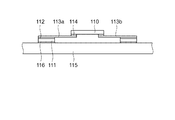
例えば、特許文献1に記載されたような従来の圧電デバイスでは、図13で示すように
、ジャイロ振動片等である圧電振動片110が、支持基板111に接合材112で固着さ
れたリード線113a、113bによって保持され導電性接着材114等で接続されてい
る。支持基板111は、パッケージ115に固着材116により固着されている。リード
線113a、113bは、2方向から圧電振動片110に接合している。
For example, in the conventional piezoelectric device described in Patent Document 1, as shown in FIG. 13, a
しかしながら、前述の背景技術に示した圧電デバイスでは、圧電振動片を支持するリー
ド線の1つずつの強度が弱いため、圧電振動片に衝撃などが印加されることによってリー
ド線が変形し、圧電振動片の保持姿勢が予期しない状態に変化することがある。この、圧
電振動片の保持姿勢の変化による特性への影響により、ジャイロ振動片の検出感度が低下
し所望の検出ができなくなるという課題を有していた。
However, in the piezoelectric device shown in the background art described above, since the strength of each lead wire supporting the piezoelectric vibrating piece is weak, the lead wire is deformed when an impact is applied to the piezoelectric vibrating piece, and the piezoelectric device is deformed. The holding posture of the vibrator element may change to an unexpected state. Due to the influence on the characteristics due to the change in the holding posture of the piezoelectric vibrating piece, there is a problem that the detection sensitivity of the gyro vibrating piece is lowered and desired detection cannot be performed.
かかる問題を解決するために、本発明の圧電デバイスは、圧電振動片と、前記圧電振動
片を保持する複数のリード線と、前記複数のリード線の一方端近傍を支持する支持基板と
、
前記複数のリード線のうちの少なくとも2つ以上のリード線を連結する連結基板と、を有
し、前記2つ以上のリード線は、前記圧電振動片を保持する部分と前記支持基板によって
支持される部分の両部分以外の部分に、前記圧電振動片と前記支持基板との接触を防止す
る間隙形成部が形成され、前記間隙形成部において前記連結基板により連結されているこ
とを特徴とする。
本発明の圧電デバイスによれば、複数のリード線が連結基板によって連結されているた
め、連結されたリード線の方が、一つずつのリード線より強度が向上し、圧電振動片に衝
撃などが印加されてもリード線の変形が起こりにくくなる。従って、圧電振動片の保持姿
勢の変化が起こりにくくなり、ジャイロ振動片の検出感度の低下を防止することができる
。
In order to solve such a problem, the piezoelectric device of the present invention includes a piezoelectric vibrating piece, a plurality of lead wires that hold the piezoelectric vibrating piece, a support substrate that supports the vicinity of one end of the plurality of lead wires,
A connection substrate that connects at least two of the plurality of lead wires, and the two or more lead wires are supported by a portion that holds the piezoelectric vibrating piece and the support substrate. A gap forming portion for preventing contact between the piezoelectric vibrating piece and the support substrate is formed in a portion other than both of the portions, and the gap forming portion is connected by the connecting substrate.
According to the piezoelectric device of the present invention, since the plurality of lead wires are connected by the connecting substrate, the strength of the connected lead wires is improved compared to one lead wire at a time. Even if is applied, deformation of the lead wire is less likely to occur. Therefore, the change in the holding posture of the piezoelectric vibrating piece is unlikely to occur, and a decrease in detection sensitivity of the gyro vibrating piece can be prevented.
また、前記間隙形成部は、前記リード線の一部を曲げて形成されていることとしてもよ
い。
Further, the gap forming portion may be formed by bending a part of the lead wire.
また、前記複数のリード線のうち前記圧電振動片と接続されていないリード線は、前記
圧電振動片に到達しない他方端を有することとしてもよい。
Moreover, the lead wire that is not connected to the piezoelectric vibrating piece among the plurality of lead wires may have the other end that does not reach the piezoelectric vibrating piece.
また、前記連結基板は、前記支持基板と同じ材質で形成されていることが望ましい。
このようにすれば、連結基板と支持基板との熱膨張係数が等しくなるため、例えば、冷
熱が繰り返し印加される、或いは、高温下に置かれるなどの熱変動による変形を防止する
ことが可能となる。
The connection board is preferably formed of the same material as the support board.
In this way, since the thermal expansion coefficients of the connection substrate and the support substrate are equal, for example, it is possible to prevent deformation due to thermal fluctuations such as repeated application of cold heat or placement at high temperatures. Become.
また、前記連結基板は、前記支持基板の一部を曲げて形成されていることとしてもよい
。
Further, the connection substrate may be formed by bending a part of the support substrate.
また、前記圧電振動片が、回転角速度を検出するためのジャイロセンサ用の振動片であ
ることとしてもよい。
Further, the piezoelectric vibrating piece may be a vibrating piece for a gyro sensor for detecting a rotational angular velocity.
また、前述の圧電デバイスと、少なくとも前記圧電デバイスを駆動するための機能を有
する回路素子と、を有することを特徴とする圧電発振器を提供することも可能となる。
It is also possible to provide a piezoelectric oscillator comprising the above-described piezoelectric device and at least a circuit element having a function for driving the piezoelectric device.
本発明に係る圧電デバイスの最良の形態について、以下に図面を用いて説明する。なお
、本発明は、後述の実施例に限定されるものではない。
(第一の実施形態)
The best mode of a piezoelectric device according to the present invention will be described below with reference to the drawings. In addition, this invention is not limited to the below-mentioned Example.
(First embodiment)
本発明に係る圧電デバイスの第一の実施形態として、ジャイロセンサ用水晶振動片(以
下、「ジャイロ振動片」という。)を用いたジャイロセンサについて、図面を用いて説明
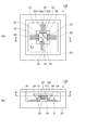
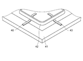
する。図1は、第一の実施形態のジャイロセンサを示す概略図である。図1(a)は、図
1(b)に示すB−B´から見たジャイロセンサの平面図である。図1(b)は、図1(
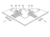
a)に示すジャイロセンサのA−A´断面図である。図2は、第一の実施形態の連結基板
とリード線とを示す図1(a)のP方向から見た斜視図である。
==ジャイロセンサの構成==
As a first embodiment of a piezoelectric device according to the present invention, a gyro sensor using a crystal vibrating piece for a gyro sensor (hereinafter referred to as “gyro vibrating piece”) will be described with reference to the drawings. FIG. 1 is a schematic view showing the gyro sensor of the first embodiment. Fig.1 (a) is a top view of the gyro sensor seen from BB 'shown in FIG.1 (b). FIG. 1 (b) shows FIG.
It is AA 'sectional drawing of the gyro sensor shown to a). FIG. 2 is a perspective view showing the connecting substrate and the lead wires of the first embodiment as seen from the P direction of FIG.
== Gyro sensor configuration ==
ジャイロセンサの構成について説明する。ジャイロセンサ100は、電子機器及び乗り
物のような物体の姿勢や位置を検出するために前記物体に搭載されて使用される。ジャイ
ロセンサ100は、水晶片であるジャイロ振動片10、直接または間接にジャイロ振動片
10を保持するための複数のリード線20、複数のリード線20を支持する支持基板21
、複数のリード線20を連結する連結基板22、当該素子を収納するためのパッケージ2
3、及びパッケージ23の蓋板24から構成される。
The configuration of the gyro sensor will be described. The
, A connecting
3 and a
セラミック等で形成されたパッケージ23の凹部底面25に、支持基板21が固着され
ている。支持基板21は、例えば、ポリイミド樹脂などで形成されている。支持基板21
の上面には、4方向から中心部26に向かって伸びる複数のリード線20が図示しない接
合材によって固着されている。複数のリード線20のうち一部のリード線20a(後述す
る接続用リード線20a)には、一方の端付近にジャイロ振動片10が導電接着剤或いは
金バンプなどの接合材27で接合されている。さらに、複数のリード線20は、立ち上が
り形状の間隙形成部28で支持基板21の一部を折り曲げて形成した連結基板22により
連結されている。
==リード線の説明==
The
A plurality of
== Description of lead wire ==
次に、複数のリード線20について説明する。
複数設けられたリード線20は、一例として厚み18μm、リード線幅30〜100μ
m、程度の銅薄板にニッケルメッキが施され形成されている。複数のリード線20は、パ
ッケージ23の凹部の4側面方向から、中心部26に向かって形成されている。複数のリ
ード線20のうち、4本がジャイロ振動片10を保持する接続用リード線20aであり、
他は、接続用リード線20aの補助用リード線20bである。複数のリード線20は、一
方の端近傍29を支持基板21上に固着されており、固着部の中途で上方に折り曲げられ
た間隙形成部28を有している。間隙形成部28は、ジャイロ振動片10と支持基板21
との間に隙間を設け、ジャイロ振動片10と支持基板21との接触を防止する。
Next, the plurality of
A plurality of
The copper thin plate of m or so is formed by nickel plating. The plurality of
The other is the
A gap is provided between the
接続用リード線20aには、さらに間隙形成部28の先のリード線端部近傍を折り曲げ
てジャイロ振動片10の受け部30が形成されている。補助用リード線20bは、間隙形
成部28の中途に一方の端部31を有している。従って、補助用リード線20bは、ジャ
イロ振動片10に接続されていない。
In the connecting
接続用リード線20a及び補助用リード線20bは、それぞれの間隙形成部28を支持
基板21の一部に形成された張り出し部を折り曲げて形成した連結基板22により連結さ
れている。連結基板22は、複数のリード線20を連結して接続用リード線20aの強度
を増加させる。
なお、連結基板22を形成するための支持基板21の張り出し部の折り曲げは、支持基
板21に固着された複数のリード線20の間隙形成部28を形成するための折り曲げと同
時に行うことができる。
The
Note that the bending of the protruding portion of the
==ジャイロ振動片の説明==
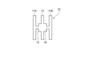
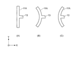
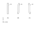
次に、ジャイロ振動片について、図面を用いて詳細に説明する。図3は、ジャイロ振動
片の平面形状の一例を示し、図1に示すジャイロ振動片10の概略の平面図である。図4
は、駆動アームの動作を示す。図5は、駆動アームの動作とコリオリ力との関係を示す。
図6は、検出アームの動作を示す。
== Description of gyro vibrating piece ==
Next, the gyro vibrating piece will be described in detail with reference to the drawings. FIG. 3 is a schematic plan view of the
Indicates the operation of the drive arm. FIG. 5 shows the relationship between the operation of the drive arm and the Coriolis force.
FIG. 6 shows the operation of the detection arm.
先ず、ジャイロ振動片の構成について説明する。
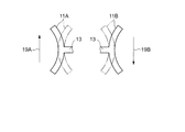
図3に示すように、ジャイロセンサ100に用いられるジャイロ振動片10は、従来知
られた駆動モード、検出モード、及びスプリアスモードという3つのモードで動作すべく
、駆動部を構成する第一の駆動腕部及び第二の駆動腕部である第一の駆動アーム11A及
び第二の駆動アーム11Bと、検出部である検出アーム12と、腕支持部であるアーム支
持部13と、支持部である支持板14とを有している。
First, the configuration of the gyro vibrating piece will be described.
As shown in FIG. 3, the
アーム支持部13は、一端が第1の駆動アーム11Aの中心に接続されており、他端が
第2の駆動アーム11Bの中心に接続されており、検出アーム12は、その中心がアーム
支持部13の中心と一致するように接続されている。支持板14は、アーム支持部13と
検出アーム12との接続点を含む所定の面積を有する板状部材である。
One end of the
次に、ジャイロ振動片の動作について説明する。
第1及び第2の駆動アーム11A、11Bは、図4(A)に示されるように、各々が図
示のY方向に延在する即ち相互に平行する、所定長を有する板状の部材である。第1及び
第2の駆動アーム11A、11Bは、図示のX方向に沿った振動中に、前記した物体の姿
勢の変動の一つである、図示のZ方向を回転軸として与えられる回転に応じて、当該回転
角速度の大きさに対応するコリオリ力を生成する。
Next, the operation of the gyro vibrating piece will be described.
As shown in FIG. 4A, the first and
駆動アーム11Aは、図4(A)〜(C)に示されるように、その中心を軸とする屈曲
動作により振動し、より詳細には、その端部に近い部位ほどX方向に沿って大きく変位す
るという凹凸型に変形することにより振動する。駆動アーム11Bは、駆動アーム11A
が変形する凹凸形状とは線対称な関係にある形状に屈曲動作により振動する。
As shown in FIGS. 4A to 4C, the drive arm 11 </ b> A vibrates due to a bending operation with its center as an axis, and more specifically, the portion closer to the end thereof becomes larger along the X direction. It vibrates by being deformed into an uneven shape that is displaced. The
Vibrates into a shape that is in a line-symmetric relationship with the concavo-convex shape that deforms by bending.
図5に示されるように、第1の駆動アーム11Aが点線で示された形状から実線で示さ
れた形状へ変化しており、第2の駆動アーム11Bも点線で示された形状から実線で示さ
れた形状へ変化しているとき、紙面内時計回り方向の回転が加えられると、コリオリ力は
、図5の矢印19A、19Bで示される方向に発生する。他方で、第1の駆動アーム11
Aが実線で示された形状から点線で示された形状へ変化し、第2の駆動アーム11Bが実
線で示された形状から点線で示された形状へ変化しているとき、紙面内時計回り方向の回
転が加えられると、コリオリ力は、図5の矢印19A、19Bとは反対方向に発生する。
As shown in FIG. 5, the
When A changes from the shape indicated by the solid line to the shape indicated by the dotted line, and the
検出アーム12は、第1の駆動アーム11A及び第2の駆動アーム11Bと同様に、図
示のY方向に沿って延在している、所定長を有する板部材である。即ち、第1の駆動アー
ム11A、第2の駆動アーム11B、及び検出アーム12は、相互に平行である。検出ア
ーム12は、第1及び第2の駆動アーム11A、11Bに働く前記コリオリ力を検出すべ
く、第1及び第2の駆動アーム11A、11Bからアーム支持部13を経て伝播される前
記コリオリ力に応答して、当該コリオリ力の大きさに対応する振動を行う。
Similar to the
検出アーム12は、図6(A)〜(C)に示されるように、図4(A)〜(C)で示し
た第1及び第2の駆動アーム11A、11Bの屈曲動作と同様に、概ねS字状及び逆S字
状に変形するという屈曲動作を行う。検出アーム12による前記屈曲動作回転により発生
する電気信号を検出することにより前記コリオリ力の大きさを知得し、これにより、前記
物品に加えられた回転角速度の大きさを認識する。
As shown in FIGS. 6 (A) to (C), the
上述の第一の実施形態によれば、ジャイロ振動片を保持し接続を行う接続用リード線と
、補助用リード線とが、連結基板によって連結されることによって、接続用リード線の強
度が増し、ジャイロ振動片に衝撃などが印加されても接続用リード線の変形が起こりにく
くなる。従って、ジャイロ振動片の保持姿勢の変化が起こりにくくなり、ジャイロ振動片
と、パッケージとの平行度が変化することから発生するジャイロ振動片の検出感度の低下
を防止することができる。
また、連結基板が、支持基板の一部である張り出し部を曲げて形成されていることから
、構成部品を増やすことなく連結することが可能となり、製品コストの増加を防ぐことが
可能となる。
(第二の実施形態)
According to the first embodiment described above, the connecting lead wire that holds and connects the gyro vibrating piece and the auxiliary lead wire are connected by the connecting substrate, thereby increasing the strength of the connecting lead wire. Even if an impact or the like is applied to the gyro vibrating piece, the connecting lead wire is hardly deformed. Therefore, the change in the holding posture of the gyro vibrating piece is less likely to occur, and it is possible to prevent the detection sensitivity of the gyro vibrating piece from being lowered due to the change in parallelism between the gyro vibrating piece and the package.
In addition, since the connecting substrate is formed by bending an overhanging portion that is a part of the support substrate, it is possible to connect without increasing the number of components, thereby preventing an increase in product cost.
(Second embodiment)
本発明に係る圧電デバイスの第二の実施形態として、圧電振動片としてジャイロ振動片
を用いたジャイロセンサについて、図面を用いて説明する。図7は、第二の実施形態のジ
ャイロセンサを示す概略図である。図7(a)は、図7(b)に示すB−B´から見たジ
ャイロセンサの平面図である。図7(b)は、図7(a)に示すジャイロセンサのA−A
´断面図である。図8は、第一の実施形態の連結基板とリード線とを示す図7(a)のP
方向から見た斜視図である。
As a second embodiment of the piezoelectric device according to the present invention, a gyro sensor using a gyro vibrating piece as a piezoelectric vibrating piece will be described with reference to the drawings. FIG. 7 is a schematic view showing the gyro sensor of the second embodiment. Fig.7 (a) is a top view of the gyro sensor seen from BB 'shown in FIG.7 (b). FIG. 7B shows an AA of the gyro sensor shown in FIG.
'Is a cross-sectional view. FIG. 8 shows the connecting substrate and the lead wires of the first embodiment.
It is the perspective view seen from the direction.
第二の実施形態におけるジャイロセンサ100の構成、及びジャイロ振動片10につい
ての説明は、先述した第一の実施形態と同様であるため省略し、第二の実施形態の特徴点
である複数のリード線40、及び連結基板42について説明する。
==リード線の説明==
The description of the configuration of the
== Description of lead wire ==
第二の実施形態の複数のリード線40について説明する。
複数のリード線40は、第一の実施形態と同様に、一例として厚み30μm、リード線
幅30〜100μm、程度の銅薄板にニッケルメッキが施されている。複数のリード線4
0は、パッケージ43の凹部の4側面方向から、中心部46に向かって形成されている。
詳細には、図7(a)に示す左右方向からそれぞれ3本、上下方向からそれぞれ1本が設
けられている。複数のリード線40は、一方の端近傍49を支持基板41上に固着されて
おり、固着部の中途で上方に折り曲げられた間隙形成部48を有している。なお、間隙形
成部48は、ジャイロ振動片10と支持基板41との間に隙間を設け、ジャイロ振動片1
0と支持基板41との接触を防止する。
The plurality of
As in the first embodiment, the plurality of
0 is formed from the four side surfaces of the concave portion of the
Specifically, three are provided from the left-right direction shown in FIG. 7A and one is provided from the vertical direction. The plurality of
The contact between 0 and the
それぞれのリード線40は、さらに間隙形成部48の先のリード線端部近傍を折り曲げ
てジャイロ振動片10の受け部50が形成されており、すべてのリード線が、ジャイロ振
動片10と接続される。この受け部50上に、ジャイロ振動片10が、金バンプ、或いは
導電性接着剤等の接合材47により固着、接続される。
さらに、それぞれのリード線40は、それぞれの間隙形成部48を連結基板42により
連結されている。
==連結基板の説明==
Each
Further, each
== Description of the connecting substrate ==
連結基板42は、それぞれのリード線40を連結してジャイロ振動片10を保持するリ
ード線40の強度を増加させる。連結基板42は、支持基板21と同じ材料で4辺を有す
るリング状に形成され、それぞれのリード線40の間隙形成部48のジャイロ振動片10
側(リード線の外側)で固着して連結する。なお、図示はしないが、連結基板42は、そ
れぞれのリード線40の間隙形成部48のパッケージ底面45側(リード線40の中心部
46に向く面)で固着して連結してもよい。
The
Secure and connect on the side (outside of the lead wire). Although not shown, the
なお、パッケージ43の上面は、蓋板44によって封止されている。
The upper surface of the
上述の第二の実施形態によれば、第一の実施形態の効果に加え、すべてのリード線を結
合することにより、ジャイロ振動片10を支持するリード線の強度を増すことが可能とな
る。
According to the second embodiment described above, in addition to the effects of the first embodiment, the strength of the lead wire that supports the
なお、図9に示すように圧電振動片を支持するためのリード線40が各方向から一つず
つ設けられる構成でも、すべてのリード線をリング状の連結基板42により一つに連結す
ることにより、ジャイロ振動片10を支持するリード線の強度を増すことが可能となる。
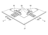
<連結基板の変形例>
Note that, as shown in FIG. 9, even in a configuration in which one
<Modified example of connection board>
連結基板の変形例を図10及び図11を用いて説明する。
図10に示すように、それぞれの方向(図10では矢印F、矢印Hで示し、F、Hに対
抗する方向を含む他の方向は省略している。)に設けられた接続用リード線20a及び補
助用リード線20bの間隙形成部28の内側に連結基板52が固着され、それぞれのリー
ド線が連結されている。連結基板52はそれぞれの方向ごと個別に設けられている。
なお、図には記載しないが、連結基板52による連結が、間隙形成部28のみでなく、
間隙形成部28からジャイロ振動片の受け部27にかかっていてもよい。
A modification of the connecting substrate will be described with reference to FIGS.
As shown in FIG. 10, the connecting
Although not shown in the figure, the connection by the
The
さらに、図11に示すように、それぞれの方向(図11では矢印F、矢印Hで示し、F、
Hに対抗する方向を含む他の方向は省略している。)に設けられた接続用リード線20a
及び補助用リード線20bの間隙形成部28の外側に連結基板52が固着され、それぞれ
のリード線が連結されている。連結基板52はそれぞれの方向ごと個別に設けられている
。
なお、図には記載しないが、連結基板52よる連結が、間隙形成部28のみでなく、間
隙形成部28から支持基板21上にかかっていてもよい。
Furthermore, as shown in FIG. 11, each direction (indicated by arrow F and arrow H in FIG.
Other directions including the direction against H are omitted. ) Connecting
And the connection board |
Although not shown in the drawing, the connection by the
なお、連結基板52の形状は、図10、図11に示す形状に限らず、間隙形成部を連結
することが可能な形状であればどのような形状であっても良い。
In addition, the shape of the connection board |
また、連結基板は、支持基板を形成する際に、連結基板の一部を連結基板とすることも
可能である。換言すれば、連結基板と支持基板を同一材質とすることが可能である。
(第三の実施形態)
In addition, when forming the support substrate, the connection substrate may be a part of the connection substrate. In other words, the connecting substrate and the supporting substrate can be made of the same material.
(Third embodiment)
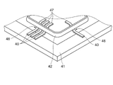
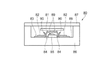
本発明の圧電振動片を用いた圧電発振器を、図を用いて説明する。図12は、本発明の
圧電振動器における概略の正面断面図である。
A piezoelectric oscillator using the piezoelectric vibrating piece of the present invention will be described with reference to the drawings. FIG. 12 is a schematic front cross-sectional view of the piezoelectric vibrator of the present invention.
本発明の圧電発振器80は、水晶片であるジャイロ振動片81、ジャイロ振動片81を
保持するための複数のリード線82、複数のリード線82を支持する支持基板83、複数
のリード線82を連結する連結基板84、少なくともジャイロ振動片81を駆動させる機
能を有する回路素子の一例としての半導体装置85、前述したそれぞれの構成部品を収納
するためのパッケージ86、及びパッケージ86の蓋板87から構成される。
The
詳述すると、セラミック等で形成されたパッケージ86の凹部底面88に、支持基板8
3が固着されている。支持基板83は、例えば、ポリイミド樹脂などで形成されている。
支持基板83の上面には、各方向から中心部に向かって伸びる複数のリード線82が図示
しない接合材によって固着されている。複数のリード線82のうち一部のリード線には一
方の端付近にジャイロ振動片81が導電接着剤或いは金バンプなどの接合材89で接合さ
れている。さらに、複数のリード線82は、立ち上がり形状の間隙形成部90で支持基板
83の一部を折り曲げて形成した連結基板84により連結されている。
More specifically, the support substrate 8 is formed on the concave bottom surface 88 of the
3 is fixed. The
A plurality of
本例によれば、ジャイロ振動片を保持し接続を行う接続用リード線と、補助用リード線
とが、連結基板によって連結されることによって、接続用リード線の強度が増し、ジャイ
ロ振動片に衝撃などが印加されても接続用リード線の変形が起こりにくくなる。従って、
ジャイロ振動片の保持姿勢の変化が起こりにくくなり、ジャイロ振動片と、パッケージと
の平行度が変化することから発生するジャイロ振動片の検出感度の低下を防止することが
できる圧電発振器を提供することが可能となる。
According to this example, the connecting lead wire that holds and connects the gyro vibrating piece and the auxiliary lead wire are connected by the connecting substrate, whereby the strength of the connecting lead wire is increased, and the gyro vibrating piece is connected to the gyro vibrating piece. Even when an impact or the like is applied, the connecting lead wire is less likely to be deformed. Therefore,
To provide a piezoelectric oscillator capable of preventing a change in the holding posture of a gyro vibrating piece and preventing a decrease in detection sensitivity of the gyro vibrating piece caused by a change in parallelism between the gyro vibrating piece and a package. Is possible.
10…ジャイロ振動片、11a…ジャイロ振動片の駆動アーム、
11b…ジャイロ振動片の駆動アーム、12…ジャイロ振動片の検出アーム、
13…ジャイロ振動片のアーム支持部、14…ジャイロ振動片の支持板、
20…複数のリード線、20a…接続用リード線、20b…補助用リード線、
21…支持基板、22…連結基板、23…パッケージ、24…蓋板、
25…パッケージの凹部底面、26…支持基板の中心部、27…接合材、
28…間隙形成部、29…リード線の一方端近傍、30…ジャイロ振動片の受け部、
31…補助用リード線の他方の端部、80…圧電発振器、100…ジャイロセンサ。
10: Gyro vibrating piece, 11a: Driving arm of the gyro vibrating piece,
11b: Gyro vibrating piece drive arm, 12: Gyro vibrating piece detection arm,
13 ... Arm support part of gyro vibrating piece, 14 ... Gyro vibrating plate support plate,
20 ... Plural lead wires, 20a ... Lead wire for connection, 20b ... Lead wire for auxiliary,
21 ... Support substrate, 22 ... Connection substrate, 23 ... Package, 24 ... Cover plate,
25 ... bottom of recess of package, 26 ... central part of support substrate, 27 ... bonding material,
28 ... Gap forming portion, 29 ... Near one end of the lead wire, 30 ... Gyro vibrating piece receiving portion,
31 ... The other end of the auxiliary lead wire, 80 ... Piezoelectric oscillator, 100 ... Gyro sensor.
Claims (7)
前記圧電振動片を保持する複数のリード線と、
前記複数のリード線の一方端近傍を支持する支持基板と、
前記複数のリード線のうちの少なくとも2つ以上のリード線を連結する連結基板と、を
有し、
前記2つ以上のリード線は、前記圧電振動片を保持する部分と前記支持基板によって支
持される部分の両部分以外の部分に、前記圧電振動片と前記支持基板との接触を防止する
間隙形成部が形成され、前記間隙形成部において前記連結基板により連結されていること
を特徴とする圧電デバイス。 A piezoelectric vibrating piece;
A plurality of lead wires for holding the piezoelectric vibrating piece;
A support substrate for supporting the vicinity of one end of the plurality of lead wires;
A connecting substrate for connecting at least two lead wires of the plurality of lead wires,
The two or more lead wires are formed with a gap for preventing contact between the piezoelectric vibrating piece and the support substrate in a portion other than both the portion holding the piezoelectric vibrating piece and the portion supported by the support substrate. The piezoelectric device is characterized in that a portion is formed and is connected by the connecting substrate in the gap forming portion.
前記間隙形成部は、前記リード線の一部を曲げて形成されていることを特徴とする圧電
デバイス。 The piezoelectric device according to claim 1,
The gap forming portion is formed by bending a part of the lead wire.
前記複数のリード線のうち前記圧電振動片と接続されていないリード線は、前記圧電振
動片に到達しない他方端を有することを特徴とする圧電デバイス。 The piezoelectric device according to claim 1,
The lead wire that is not connected to the piezoelectric vibrating piece among the plurality of lead wires has the other end that does not reach the piezoelectric vibrating piece.
前記連結基板は、前記支持基板と同じ材質で形成されていることを特徴とする圧電デバ
イス。 The piezoelectric device according to claim 1,
The piezoelectric device is characterized in that the connection substrate is formed of the same material as the support substrate.
前記連結基板は、前記支持基板の一部を曲げて形成されていることを特徴とする圧電デ
バイス。 The piezoelectric device according to claim 1,
The connecting substrate is formed by bending a part of the support substrate.
前記圧電振動片が、回転角速度を検出するためのジャイロセンサ用の振動片であること
を特徴とする圧電デバイス。 The piezoelectric device according to claim 1,
The piezoelectric device, wherein the piezoelectric vibrating piece is a vibrating piece for a gyro sensor for detecting a rotational angular velocity.
少なくとも前記圧電デバイスを駆動するための機能を有する回路素子と、
を有することを特徴とする圧電発振器。
A piezoelectric device according to claim 1;
A circuit element having a function for driving at least the piezoelectric device;
A piezoelectric oscillator comprising:
Priority Applications (1)
| Application Number | Priority Date | Filing Date | Title |
|---|---|---|---|
| JP2004111075A JP2005292079A (en) | 2004-04-05 | 2004-04-05 | Piezoelectric device and piezoelectric oscillator |
Applications Claiming Priority (1)
| Application Number | Priority Date | Filing Date | Title |
|---|---|---|---|
| JP2004111075A JP2005292079A (en) | 2004-04-05 | 2004-04-05 | Piezoelectric device and piezoelectric oscillator |
Publications (1)
| Publication Number | Publication Date |
|---|---|
| JP2005292079A true JP2005292079A (en) | 2005-10-20 |
Family
ID=35325155
Family Applications (1)
| Application Number | Title | Priority Date | Filing Date |
|---|---|---|---|
| JP2004111075A Withdrawn JP2005292079A (en) | 2004-04-05 | 2004-04-05 | Piezoelectric device and piezoelectric oscillator |
Country Status (1)
| Country | Link |
|---|---|
| JP (1) | JP2005292079A (en) |
Cited By (13)
| Publication number | Priority date | Publication date | Assignee | Title |
|---|---|---|---|---|
| JP2008076153A (en) * | 2006-09-20 | 2008-04-03 | Denso Corp | Mechanical quantity sensor |
| JP2010190706A (en) * | 2009-02-18 | 2010-09-02 | Panasonic Corp | Inertial force sensor |
| US7978016B2 (en) | 2008-08-19 | 2011-07-12 | Nihon Dempa Kogyo Co., Ltd | Crystal oscillator |
| EP2363689A2 (en) | 2010-03-01 | 2011-09-07 | Seiko Epson Corporation | Motion sensor, and method of manufacturing motion sensor |
| JP2012078103A (en) * | 2010-09-30 | 2012-04-19 | Seiko Epson Corp | Sensor module, sensor device, method for manufacturing sensor device, and electronic apparatus |
| US8501538B2 (en) | 2011-01-21 | 2013-08-06 | Seiko Epson Corporation | Method for connecting substrate and method for manufacturing semiconductor device |
| CN103363975A (en) * | 2012-03-29 | 2013-10-23 | 精工爱普生株式会社 | Vibration device and method for manufacturing vibration device |
| US8631701B2 (en) | 2010-09-30 | 2014-01-21 | Seiko Epson Corporation | Sensor device, motion sensor, and electronic device |
| US8749001B2 (en) | 2010-09-30 | 2014-06-10 | Seiko Epson Corporation | Electronic component, electronic device, and method of manufacturing the electronic component |
| JP2014222233A (en) * | 2014-06-24 | 2014-11-27 | セイコーエプソン株式会社 | Sensor device and motion sensor |
| US9088262B2 (en) | 2011-03-03 | 2015-07-21 | Seiko Epson Corporation | Vibrating device, method for manufacturing vibrating device, and electronic apparatus |
| US9568313B2 (en) | 2014-10-28 | 2017-02-14 | Seiko Epson Corporation | Electronic device, electronic apparatus, and moving object |
| JP2017078630A (en) * | 2015-10-20 | 2017-04-27 | セイコーエプソン株式会社 | Physical quantity detection device, electronic apparatus and movable body |
-
2004
- 2004-04-05 JP JP2004111075A patent/JP2005292079A/en not_active Withdrawn
Cited By (15)
| Publication number | Priority date | Publication date | Assignee | Title |
|---|---|---|---|---|
| JP2008076153A (en) * | 2006-09-20 | 2008-04-03 | Denso Corp | Mechanical quantity sensor |
| US7978016B2 (en) | 2008-08-19 | 2011-07-12 | Nihon Dempa Kogyo Co., Ltd | Crystal oscillator |
| US8857258B2 (en) | 2009-02-18 | 2014-10-14 | Panasonic Corporation | Inertial force sensor |
| JP2010190706A (en) * | 2009-02-18 | 2010-09-02 | Panasonic Corp | Inertial force sensor |
| EP2363689A2 (en) | 2010-03-01 | 2011-09-07 | Seiko Epson Corporation | Motion sensor, and method of manufacturing motion sensor |
| US8631701B2 (en) | 2010-09-30 | 2014-01-21 | Seiko Epson Corporation | Sensor device, motion sensor, and electronic device |
| US8749001B2 (en) | 2010-09-30 | 2014-06-10 | Seiko Epson Corporation | Electronic component, electronic device, and method of manufacturing the electronic component |
| JP2012078103A (en) * | 2010-09-30 | 2012-04-19 | Seiko Epson Corp | Sensor module, sensor device, method for manufacturing sensor device, and electronic apparatus |
| US8501538B2 (en) | 2011-01-21 | 2013-08-06 | Seiko Epson Corporation | Method for connecting substrate and method for manufacturing semiconductor device |
| US9088262B2 (en) | 2011-03-03 | 2015-07-21 | Seiko Epson Corporation | Vibrating device, method for manufacturing vibrating device, and electronic apparatus |
| CN103363975A (en) * | 2012-03-29 | 2013-10-23 | 精工爱普生株式会社 | Vibration device and method for manufacturing vibration device |
| JP2014222233A (en) * | 2014-06-24 | 2014-11-27 | セイコーエプソン株式会社 | Sensor device and motion sensor |
| US9568313B2 (en) | 2014-10-28 | 2017-02-14 | Seiko Epson Corporation | Electronic device, electronic apparatus, and moving object |
| US10302430B2 (en) | 2014-10-28 | 2019-05-28 | Seiko Epson Corporation | Electronic device, electronic apparatus, and moving object |
| JP2017078630A (en) * | 2015-10-20 | 2017-04-27 | セイコーエプソン株式会社 | Physical quantity detection device, electronic apparatus and movable body |
Similar Documents
| Publication | Publication Date | Title |
|---|---|---|
| JP3966237B2 (en) | Piezoelectric devices and electronic devices equipped with piezoelectric devices | |
| JP2005292079A (en) | Piezoelectric device and piezoelectric oscillator | |
| JP2006078248A (en) | Physical quantity sensor device | |
| JP6620243B2 (en) | Angular velocity sensor, sensor element and multi-axis angular velocity sensor | |
| US11885621B2 (en) | Sensor device | |
| JP2021067701A (en) | Angular velocity sensor and sensor element | |
| WO2019240175A1 (en) | Sensor element and angular velocity sensor | |
| JP4682671B2 (en) | Piezoelectric device | |
| JP4379478B2 (en) | Piezoelectric devices and electronic devices equipped with piezoelectric devices. | |
| JP2006029799A (en) | Piezoelectric device and piezoelectric oscillator | |
| JP2005345354A (en) | Piezoelectric device and piezoelectric oscillator | |
| CN103363967A (en) | Vibration device | |
| JP7089590B2 (en) | Sensor element and angular velocity sensor | |
| JP2006234463A (en) | Inertial sensor | |
| JP4367488B2 (en) | Method for manufacturing piezoelectric device | |
| JP2004138390A (en) | Oscillator support structure | |
| JP2008281586A (en) | Vibrator support mechanism and vibrator unit | |
| JP2009099822A (en) | Physical quantity detection device | |
| EP1895269A2 (en) | Vibration sensor | |
| JP2007316090A (en) | Inertial sensor | |
| JP2005308608A (en) | Piezoelectric device, method for manufacturing piezoelectric device, and piezoelectric oscillator | |
| JPWO2014002416A1 (en) | Strain sensor | |
| JP2010266320A (en) | Angular velocity sensor device and manufacturing method thereof | |
| JP2007316091A (en) | Inertial sensor | |
| US20080105051A1 (en) | Vibration sensor and method for manufacturing the same |
Legal Events
| Date | Code | Title | Description |
|---|---|---|---|
| A300 | Application deemed to be withdrawn because no request for examination was validly filed |
Free format text: JAPANESE INTERMEDIATE CODE: A300 Effective date: 20070605 |