EP1487060A2 - Technique for interconnecting multilayer circuit boards - Google Patents
Technique for interconnecting multilayer circuit boards Download PDFInfo
- Publication number
- EP1487060A2 EP1487060A2 EP04394034A EP04394034A EP1487060A2 EP 1487060 A2 EP1487060 A2 EP 1487060A2 EP 04394034 A EP04394034 A EP 04394034A EP 04394034 A EP04394034 A EP 04394034A EP 1487060 A2 EP1487060 A2 EP 1487060A2
- Authority
- EP
- European Patent Office
- Prior art keywords
- circuit board
- electrically conductive
- pins
- multilayer circuit
- conductive vias
- Prior art date
- Legal status (The legal status is an assumption and is not a legal conclusion. Google has not performed a legal analysis and makes no representation as to the accuracy of the status listed.)
- Withdrawn
Links
Images

Classifications
-
- H—ELECTRICITY
- H01—ELECTRIC ELEMENTS
- H01R—ELECTRICALLY-CONDUCTIVE CONNECTIONS; STRUCTURAL ASSOCIATIONS OF A PLURALITY OF MUTUALLY-INSULATED ELECTRICAL CONNECTING ELEMENTS; COUPLING DEVICES; CURRENT COLLECTORS
- H01R12/00—Structural associations of a plurality of mutually-insulated electrical connecting elements, specially adapted for printed circuits, e.g. printed circuit boards [PCB], flat or ribbon cables, or like generally planar structures, e.g. terminal strips, terminal blocks; Coupling devices specially adapted for printed circuits, flat or ribbon cables, or like generally planar structures; Terminals specially adapted for contact with, or insertion into, printed circuits, flat or ribbon cables, or like generally planar structures
- H01R12/50—Fixed connections
- H01R12/51—Fixed connections for rigid printed circuits or like structures
- H01R12/52—Fixed connections for rigid printed circuits or like structures connecting to other rigid printed circuits or like structures
- H01R12/523—Fixed connections for rigid printed circuits or like structures connecting to other rigid printed circuits or like structures by an interconnection through aligned holes in the boards or multilayer board
-
- H—ELECTRICITY
- H05—ELECTRIC TECHNIQUES NOT OTHERWISE PROVIDED FOR
- H05K—PRINTED CIRCUITS; CASINGS OR CONSTRUCTIONAL DETAILS OF ELECTRIC APPARATUS; MANUFACTURE OF ASSEMBLAGES OF ELECTRICAL COMPONENTS
- H05K1/00—Printed circuits
- H05K1/02—Details
- H05K1/14—Structural association of two or more printed circuits
-
- H—ELECTRICITY
- H05—ELECTRIC TECHNIQUES NOT OTHERWISE PROVIDED FOR
- H05K—PRINTED CIRCUITS; CASINGS OR CONSTRUCTIONAL DETAILS OF ELECTRIC APPARATUS; MANUFACTURE OF ASSEMBLAGES OF ELECTRICAL COMPONENTS
- H05K3/00—Apparatus or processes for manufacturing printed circuits
- H05K3/36—Assembling printed circuits with other printed circuits
- H05K3/368—Assembling printed circuits with other printed circuits parallel to each other
-
- H—ELECTRICITY
- H05—ELECTRIC TECHNIQUES NOT OTHERWISE PROVIDED FOR
- H05K—PRINTED CIRCUITS; CASINGS OR CONSTRUCTIONAL DETAILS OF ELECTRIC APPARATUS; MANUFACTURE OF ASSEMBLAGES OF ELECTRICAL COMPONENTS
- H05K3/00—Apparatus or processes for manufacturing printed circuits
- H05K3/46—Manufacturing multilayer circuits
-
- H—ELECTRICITY
- H01—ELECTRIC ELEMENTS
- H01R—ELECTRICALLY-CONDUCTIVE CONNECTIONS; STRUCTURAL ASSOCIATIONS OF A PLURALITY OF MUTUALLY-INSULATED ELECTRICAL CONNECTING ELEMENTS; COUPLING DEVICES; CURRENT COLLECTORS
- H01R12/00—Structural associations of a plurality of mutually-insulated electrical connecting elements, specially adapted for printed circuits, e.g. printed circuit boards [PCB], flat or ribbon cables, or like generally planar structures, e.g. terminal strips, terminal blocks; Coupling devices specially adapted for printed circuits, flat or ribbon cables, or like generally planar structures; Terminals specially adapted for contact with, or insertion into, printed circuits, flat or ribbon cables, or like generally planar structures
- H01R12/50—Fixed connections
- H01R12/51—Fixed connections for rigid printed circuits or like structures
- H01R12/55—Fixed connections for rigid printed circuits or like structures characterised by the terminals
- H01R12/57—Fixed connections for rigid printed circuits or like structures characterised by the terminals surface mounting terminals
-
- H—ELECTRICITY
- H01—ELECTRIC ELEMENTS
- H01R—ELECTRICALLY-CONDUCTIVE CONNECTIONS; STRUCTURAL ASSOCIATIONS OF A PLURALITY OF MUTUALLY-INSULATED ELECTRICAL CONNECTING ELEMENTS; COUPLING DEVICES; CURRENT COLLECTORS
- H01R13/00—Details of coupling devices of the kinds covered by groups H01R12/70 or H01R24/00 - H01R33/00
- H01R13/64—Means for preventing incorrect coupling
- H01R13/642—Means for preventing incorrect coupling by position or shape of contact members
-
- H—ELECTRICITY
- H01—ELECTRIC ELEMENTS
- H01R—ELECTRICALLY-CONDUCTIVE CONNECTIONS; STRUCTURAL ASSOCIATIONS OF A PLURALITY OF MUTUALLY-INSULATED ELECTRICAL CONNECTING ELEMENTS; COUPLING DEVICES; CURRENT COLLECTORS
- H01R13/00—Details of coupling devices of the kinds covered by groups H01R12/70 or H01R24/00 - H01R33/00
- H01R13/66—Structural association with built-in electrical component
- H01R13/665—Structural association with built-in electrical component with built-in electronic circuit
-
- H—ELECTRICITY
- H05—ELECTRIC TECHNIQUES NOT OTHERWISE PROVIDED FOR
- H05K—PRINTED CIRCUITS; CASINGS OR CONSTRUCTIONAL DETAILS OF ELECTRIC APPARATUS; MANUFACTURE OF ASSEMBLAGES OF ELECTRICAL COMPONENTS
- H05K2201/00—Indexing scheme relating to printed circuits covered by H05K1/00
- H05K2201/09—Shape and layout
- H05K2201/09209—Shape and layout details of conductors
- H05K2201/09372—Pads and lands
- H05K2201/09472—Recessed pad for surface mounting; Recessed electrode of component
-
- H—ELECTRICITY
- H05—ELECTRIC TECHNIQUES NOT OTHERWISE PROVIDED FOR
- H05K—PRINTED CIRCUITS; CASINGS OR CONSTRUCTIONAL DETAILS OF ELECTRIC APPARATUS; MANUFACTURE OF ASSEMBLAGES OF ELECTRICAL COMPONENTS
- H05K2201/00—Indexing scheme relating to printed circuits covered by H05K1/00
- H05K2201/09—Shape and layout
- H05K2201/09209—Shape and layout details of conductors
- H05K2201/095—Conductive through-holes or vias
- H05K2201/09536—Buried plated through-holes, i.e. plated through-holes formed in a core before lamination
-
- H—ELECTRICITY
- H05—ELECTRIC TECHNIQUES NOT OTHERWISE PROVIDED FOR
- H05K—PRINTED CIRCUITS; CASINGS OR CONSTRUCTIONAL DETAILS OF ELECTRIC APPARATUS; MANUFACTURE OF ASSEMBLAGES OF ELECTRICAL COMPONENTS
- H05K2201/00—Indexing scheme relating to printed circuits covered by H05K1/00
- H05K2201/10—Details of components or other objects attached to or integrated in a printed circuit board
- H05K2201/10613—Details of electrical connections of non-printed components, e.g. special leads
- H05K2201/10621—Components characterised by their electrical contacts
- H05K2201/10659—Different types of terminals for the same component, e.g. solder balls combined with leads
-
- H—ELECTRICITY
- H05—ELECTRIC TECHNIQUES NOT OTHERWISE PROVIDED FOR
- H05K—PRINTED CIRCUITS; CASINGS OR CONSTRUCTIONAL DETAILS OF ELECTRIC APPARATUS; MANUFACTURE OF ASSEMBLAGES OF ELECTRICAL COMPONENTS
- H05K2203/00—Indexing scheme relating to apparatus or processes for manufacturing printed circuits covered by H05K3/00
- H05K2203/06—Lamination
- H05K2203/061—Lamination of previously made multilayered subassemblies
-
- H—ELECTRICITY
- H05—ELECTRIC TECHNIQUES NOT OTHERWISE PROVIDED FOR
- H05K—PRINTED CIRCUITS; CASINGS OR CONSTRUCTIONAL DETAILS OF ELECTRIC APPARATUS; MANUFACTURE OF ASSEMBLAGES OF ELECTRICAL COMPONENTS
- H05K3/00—Apparatus or processes for manufacturing printed circuits
- H05K3/30—Assembling printed circuits with electric components, e.g. with resistors
- H05K3/32—Assembling printed circuits with electric components, e.g. with resistors electrically connecting electric components or wires to printed circuits
- H05K3/34—Assembling printed circuits with electric components, e.g. with resistors electrically connecting electric components or wires to printed circuits by soldering
- H05K3/341—Surface mounted components
- H05K3/3431—Leadless components
- H05K3/3436—Leadless components having an array of bottom contacts, e.g. pad grid array or ball grid array components
-
- H—ELECTRICITY
- H05—ELECTRIC TECHNIQUES NOT OTHERWISE PROVIDED FOR
- H05K—PRINTED CIRCUITS; CASINGS OR CONSTRUCTIONAL DETAILS OF ELECTRIC APPARATUS; MANUFACTURE OF ASSEMBLAGES OF ELECTRICAL COMPONENTS
- H05K3/00—Apparatus or processes for manufacturing printed circuits
- H05K3/30—Assembling printed circuits with electric components, e.g. with resistors
- H05K3/32—Assembling printed circuits with electric components, e.g. with resistors electrically connecting electric components or wires to printed circuits
- H05K3/34—Assembling printed circuits with electric components, e.g. with resistors electrically connecting electric components or wires to printed circuits by soldering
- H05K3/3447—Lead-in-hole components
-
- H—ELECTRICITY
- H05—ELECTRIC TECHNIQUES NOT OTHERWISE PROVIDED FOR
- H05K—PRINTED CIRCUITS; CASINGS OR CONSTRUCTIONAL DETAILS OF ELECTRIC APPARATUS; MANUFACTURE OF ASSEMBLAGES OF ELECTRICAL COMPONENTS
- H05K3/00—Apparatus or processes for manufacturing printed circuits
- H05K3/36—Assembling printed circuits with other printed circuits
- H05K3/361—Assembling flexible printed circuits with other printed circuits
- H05K3/365—Assembling flexible printed circuits with other printed circuits by abutting, i.e. without alloying process
-
- H—ELECTRICITY
- H05—ELECTRIC TECHNIQUES NOT OTHERWISE PROVIDED FOR
- H05K—PRINTED CIRCUITS; CASINGS OR CONSTRUCTIONAL DETAILS OF ELECTRIC APPARATUS; MANUFACTURE OF ASSEMBLAGES OF ELECTRICAL COMPONENTS
- H05K3/00—Apparatus or processes for manufacturing printed circuits
- H05K3/40—Forming printed elements for providing electric connections to or between printed circuits
- H05K3/42—Plated through-holes or plated via connections
- H05K3/429—Plated through-holes specially for multilayer circuits, e.g. having connections to inner circuit layers
-
- Y—GENERAL TAGGING OF NEW TECHNOLOGICAL DEVELOPMENTS; GENERAL TAGGING OF CROSS-SECTIONAL TECHNOLOGIES SPANNING OVER SEVERAL SECTIONS OF THE IPC; TECHNICAL SUBJECTS COVERED BY FORMER USPC CROSS-REFERENCE ART COLLECTIONS [XRACs] AND DIGESTS
- Y10—TECHNICAL SUBJECTS COVERED BY FORMER USPC
- Y10T—TECHNICAL SUBJECTS COVERED BY FORMER US CLASSIFICATION
- Y10T409/00—Gear cutting, milling, or planing
- Y10T409/30—Milling
- Y10T409/300056—Thread or helix generating
- Y10T409/300112—Process
-
- Y—GENERAL TAGGING OF NEW TECHNOLOGICAL DEVELOPMENTS; GENERAL TAGGING OF CROSS-SECTIONAL TECHNOLOGIES SPANNING OVER SEVERAL SECTIONS OF THE IPC; TECHNICAL SUBJECTS COVERED BY FORMER USPC CROSS-REFERENCE ART COLLECTIONS [XRACs] AND DIGESTS
- Y10—TECHNICAL SUBJECTS COVERED BY FORMER USPC
- Y10T—TECHNICAL SUBJECTS COVERED BY FORMER US CLASSIFICATION
- Y10T409/00—Gear cutting, milling, or planing
- Y10T409/30—Milling
- Y10T409/300056—Thread or helix generating
- Y10T409/300616—Work means to move work axially and means to interrelate work movement with cutter rotation
Definitions
- the present invention relates generally to connecting multiple circuit boards and, more particularly, to a technique for interconnecting two or more multilayer circuit boards having vias of varying depths.
- PCBs printed circuit boards
- multilayer PCBs may be either single or double-sided and may have multiple signal layers on the surface of and buried within the multilayer PCBs.
- these intrinsic parasitics can also have an adverse effect on the manufacturability of a PCB and thus the cost thereof. Because of their adverse affect on signal performance, these intrinsic parasitics can also limit the bandwidth of signals propagating along each electrically conductive via. These adverse affects only increase as the number of layers in a multilayer PCB increase.
- Kwong et al. disclose a technique for manufacturing and using a PCB wherein certain vias extend only through a subset of the layers of the PCB to create channels in the portions of the PCB where vias are absent. These channels then may be used to route a larger number of signal, power, ground and/or test traces between vias thereby reducing the number of layers necessary to provide a certain number of electrical connections.
- a circuit device for interconnecting first and second multilayer circuit boards is provided in accordance with one embodiment of the present invention.
- the first multilayer circuit board has a first plurality of electrically conductive vias of varying depths and the second multilayer circuit board has a second plurality of electrically conductive vias.
- the circuit device comprises a first plurality of pins located on a first side of the circuit device corresponding to the first plurality of electrically conductive vias of the first multilayer circuit board, each pin having a length compatible with a depth of a respective one of the first plurality of electrically conductive vias of the first multilayer circuit board.
- the circuit device further comprises a second plurality of pins located on a second side of the circuit device corresponding to the second plurality of electrically conductive vias of the second multilayer circuit board.
- a circuit module is provided in accordance with another embodiment of the present invention.
- the circuit module comprises a first multilayer circuit board having a first plurality of electrically conductive vias of varying depths and a second multilayer circuit board having a second plurality of electrically conductive vias.
- the circuit module further comprises a circuit device having a first side mounted to a surface of the first multilayer circuit board and a second side mounted to a surface of the second multilayer circuit board.
- the circuit device comprises a first plurality of pins located on the first side of the circuit device corresponding to the first plurality of electrically conductive vias of the first multilayer circuit board, each pin extending into and in electrical contact with a respective one of the first plurality of electrically conductive vias of the first multilayer circuit board and a second plurality of pins located on the second side of the circuit device corresponding to the second plurality of vias of the second multilayer circuit board, each pin extending into and in electrical contact with a respective one of the second plurality of electrically conductive vias of the second multilayer circuit board, wherein each of the first plurality of pins of the circuit device has a length compatible with a depth of a respective one of the first plurality of electrically conductive vias of the first multilayer circuit board.
- a method for implementing a circuit device to interconnect at least first and second multilayer circuit boards is provided in accordance with another embodiment of the present invention.
- the circuit device includes a first plurality of pins located on a first surface of the circuit device and a second plurality of pins located on a second surface of the circuit device, the first multilayer circuit board includes a first plurality of electrically conductive vias of varying depths and the second multilayer circuit board having a second plurality of electrically conductive vias.
- the method comprising the step of forming at least one pin of the first plurality of pins of the circuit device to have a length compatible with a depth of a respective one of the first plurality of electrically conductive vias of the first multilayer circuit board.
- the method further comprises the steps of joining the first surface of the circuit device to a surface of the first multilayer circuit board, each pin of the first plurality of pins extending into and being in electrical contact with a respective one of the first plurality of electrically conductive vias of the first multilayer circuit board and joining the second surface of the circuit device to a surface of the second multilayer circuit board, each pin of the second plurality of pins extending into and being in electrical contact with a respective one of the second plurality of electrically conductive vias of the second multilayer circuit board.
- Figures 1A-3 illustrate various exemplary techniques for interconnecting two or more PCBs using a double-sided pin device.
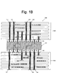
- Figures 1A and 1B illustrate an exemplary technique for implementing a double-sided through hole-based pin device, such as a pin grid array (PGA) package, to interconnect two PCBs, at least one of which incorporates vias of varying depths.
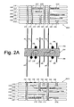
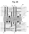
- Figures 2A and 2B illustrate an exemplary technique for implementing a double-sided hybrid pin device to interconnect two PCBs, at least one of which incorporates vias of varying depths.
- PGA pin grid array
- hybrid pin device typically refers to a circuit device that utilizes both through hole-based pins (e.g., PGA) and surface mount (SMT) pins (e.g., column grid array (CGA) or ball grid array (BGA)).
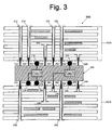
- Figure 3 illustrates a circuit module having two PCBs interconnected by a double-sided pin device having subsets of pins of uniform length.
- Figures 1A-3 illustrate exemplary embodiments wherein double-sided pin devices are used to join two PCBs, each having vias of varying depths to facilitate channel routing, in other embodiments, the techniques described herein may be used to join PCBs having vias of various depths for reasons other than, or in addition to, channel routing.
- pin may refer to any of a variety of conductive structures (e.g., "leads") used to provide an electrical connection between one or more electrical conduits of a PCB and an input/output of a pin device.
- Examples of pins may include, but are not limited to, straight pins, metal (e.g., gold) dendrites pins, balls, columns, etc.
- FIG. 1A an exemplary technique for interconnecting two PCBs, at least one of which having vias of varying depths, using a double-sided pin device is illustrated in accordance with at least one embodiment of the present invention.
- a cross-section view of a circuit module including a PCB 102A, a PCB 102B and a through hole-based pin device 150 is illustrated prior to assembly.
- the cross-section view is assumed to occur at a row of pins of the device 150 and the corresponding rows of the PCBs 102A and 102B.
- the PCB 102A comprises alternating dielectric layers 104A-104F and conductive layers 106A-106E.
- the PCB 102B comprises alternating dielectric layers 128A-128F and conductive layers 130A-130E.
- PCBs 102A and 102B are illustrated as having a certain number of layers, PCBs having any number of layers may be implemented, as appropriate, using the guidelines provided herein.
- one or more channel routing techniques may be implemented to determine an optimal channel routing scheme for one or both of the PCBs 102A and 102B.
- the channel routing technique described by Kwong et al. in U.S. Patent No. 6,388,890 preferably is used.
- channels for routing signal traces (also referred to as lines or runs) may be formed by utilizing vias that only partially penetrate the PCB. The portions of the unpenetrated layers beneath the via, i.e., the channels, may then be used to route signal traces.
- the exemplary PCB 102A having vias 112-122 and 126 and surface pad 124 at the illustrated row may be formed as a result of one or more channel routing process such as the one disclosed by Kwong et al., where vias 112, 114, 120 and 122 include through holes penetrating through the entirety of the PCB 102A and vias 116, 118 and 126 include blind vias (e.g., microvias) that penetrate only a subset of the layers of the PCB 102A.
- This exemplary configuration may provide for the formation of one or more channels at various layers of the PCB 102A, such as, for example, channels 108A-108E.
- the channels 108A-108E then may be utilized to run traces at the corresponding layers of the PCB 102A as described by, for example, Kwong et al.
- both of PCBs 102A and 102B implement channel routing. Accordingly, vias 132 and 138-146 and surface pads 134 and 136 may be arranged at the respective row of the PCB 102B so as to create channels 110A-110H at various layers of PCB 102B in a manner as described above. Vias and surface pads may be arranged in a similar manner at other rows. The channels 110A-110H then may be used to route traces in accordance with the desired operation of the resulting circuit device.
- vias of varying depths preferably includes the implementation of channels for routing signal traces
- the present invention may be applied to interconnect circuit boards having vias of varying depths for reasons other than channel routing without departing from the spirit or the scope of the present invention.
- the device 150 may include any of a variety of through hole-based circuit devices, such as a dual-inline package (DIP), a PGA package, chip scale package (CSP), through hole array connectors, and the like.
- the device 150 includes a plurality of pins located on the top surface 168 and a plurality of pins located on the bottom surface 188. Some or all of the pins may be electrically connected to one or more inputs and/or outputs of the circuitry of the device 150.
- the pins preferably are arranged on each respective surface in a grid (or "matrix") pattern.
- pins 152-166 corresponding to vias/surface pads 112-126, respectively
- pins 172-186 corresponding to vias/surface pads 132-146, respectively
- a circuit device having the arrangement of pins located on both the top surface and the bottom surface of the device is herein referred to as a double-sided pin device.
- Double-sided devices typically are constructed with pins of uniform length.
- PCBs implementing vias of varying lengths for channel routing or other purposes may necessitate the use of pins of various lengths.
- vias 112, 114, 120, 122, 132, 142 and 144 are, in this example, through holes, full-length pins may be used on the locations of the device 150 that correspond to these vias (i.e., are intended to provide an electrical connection with these vias).
- PCBs typically incorporate blind vias (e.g., vias 116, 118, 126, 138, 140 and 146) and/or surface pads (e.g., surface pads 124, 134 and 136) to form channels or for other reasons, full-length pins that are appropriate for through-holes may not be suitable for the blind vias/surface pads.
- blind vias e.g., vias 116, 118, 126, 138, 140 and 14
- surface pads e.g., surface pads 124, 134 and 13
- the pins of the device 150 may be formed at the time of manufacture or modified after manufacture to have lengths compatible with the corresponding vias/surface pads of the PCBs 102A and 102B.
- a pin preferably is compatible with the corresponding via when its length is sufficient to allow the pin to form a reliable mechanical attachment and electrical contact with the via when the device 150 is mounted on the surface of the PCB (e.g., by extending at least partially into the via) but not so long as to prevent other pins from forming reliable mechanical attachments and electrical contacts with their corresponding vias or surface pads.
- the "depth" of the surface pad may be represented as the distance between the outer (in this case top) surface of the device 150 and the corresponding surface pad.
- the device 150 may be manufactured as a general-purpose device having pins 152-166 and 172-186 of a uniform length suitable for PCBs having through holes only.
- portions of certain pins may be removed so that the modified pin has a length compatible with the depth of the corresponding via/surface pad.
- portions 156A, 158A, 164A, 166A, 174A, 176A, 178A, 180A and 186A may be trimmed from the pins 156, 158, 164, 166, 174, 176, 178, 180 and 186, respectively.
- the resulting pin configuration of the device 150 allows the pins 152-162, 166, 172 and 178-186 to extend substantially into and come into electrical contact with the corresponding via (vias 112-122, 126, 132 and 138-146, respectively) and allows the pins 164, 174 and 176 to come in electrical contact with the corresponding surface pad of the corresponding PCB.
- any of a variety of methods may be utilized to form the pins of the device 150 to the appropriate length. Such techniques may include, for example, trimming the pins to the desired length using a diamond saw or laser cutting device, grinding the pins down to their desired lengths, and the like. Alternatively, the pins may be formed at time of manufacture to have the appropriate length.
- the device 150 preferably is used to provide one or more electrical connections between the PCB 102A and the PCB 102B after assembly. Accordingly, the device 150 preferably includes logic to provide a connection between one or more pins of the top surface 168 and one or more pins of the bottom surface 188. For example, the device 150 may include logic 192 to provide a connection between the pins 156, 174 and 176 and logic 194 to provide a connection between the pins 164 and 180.
- This logic may include any combination of passive and active circuitry.
- the logic may include a simple conductive path to provide a signal conduit between a pin of the top surface and a pin of the bottom surface.
- the logic may include, for example, filtering circuitry to reduce noise in a signal transmitted between a pin of the top surface 168 and a pin of the bottom surface 188.
- the logic may include, for example, active circuitry related to the intended operation of the device such as, for example, digital signal processing (DSP) logic.
- DSP digital signal processing
- Figure 1B illustrates an exemplary assembly of the device 150 and PCBs 102A and 102B of Figure 1A to form a circuit module 190 in accordance with at least one embodiment of the present invention.
- the pins 152-162, 166 may be inserted into and brought into electrical contact with the corresponding vias 112-122, 126, respectively, of the PCB 102A and the pins 172, 178-186 may be inserted into and brought into electrical contact with the corresponding vias 132, 138-146, respectively, of the PCB 102B.
- pin 164 may be brought into electrical contact with surface pad 124 of PCB 102A and pins 174, 176 may be brought into electrical contact with surface pads 134, 136, respectively, of PCB 102B.
- Electrical and/or mechanical coupling between a pin and the corresponding via/surface pad may be accomplished using any of a variety of means known to those skilled in the art.
- the pins may be soldered to their corresponding via/surface pad using a solder reflow technique.
- the device 150 may be keyed to prevent an incorrect orientation during assembly.
- a pin location on one of the PCBs 102A, 102B and the corresponding pin of the device 150 may be keyed with a particular shape (e.g., a square) that differentiates them from the remainder of the pins/pads which share a different shape (e.g., circular).
- the device 150 may be keyed by using a certain pin pattern for the top outer surface that is incompatible with the PCB 102B or a pin pattern for the bottom outer surface that is incompatible with the PCB 102A.
- the device 150 may implement certain mechanical or structural features, such as a ridge or a notch, that prevent the device 150 from being incorrectly inserted into the PCB 102A/PCB 102B.
- the device 150 functions as a connector between the PCB 102A and the PCB 102B. Unlike simple mechanical connectors, however, the pin device 150 may implement passive or active logic to reduce or eliminate negative effects in signals transmitted between the PCB 102A and the PCB 102B. Further, the connection of a double-sided pin device to multiple PCBS may reduce the cost and complexity of the circuit device in many instances.
- FIG. 2A an exemplary technique for interconnecting two channel-routed PCBs using a double-sided hybrid pin device is illustrated in accordance with at least one embodiment of the present invention.
- a cross-section view of a circuit module including a PCB 202A, a PCB 202B and a hybrid device 250 is illustrated prior to assembly.
- the cross-section view is assumed to occur at a row of pins of the device 250 and the corresponding rows of the PCBs 202A and 202B.
- the PCB 202A comprises alternating dielectric layers 204A-204F and conductive layers 206A-206E.
- the PCB 202B (comprises alternating dielectric layers 228A-228F and conductive layers 230A-230E.
- PCBs 202A and 202B are illustrated as having a certain number of layers, PCBs having any number of layers may be implemented, as appropriate, using the guidelines provided herein.
- the PCBs 202A and 202B may incorporate channel routing using an arrangement of vias of varying depths, such as through holes, blind vias and/or surface pads.
- the PCB 202A uses through holes 212, 214, 220 and 222, blind vias 218 and 226, and surface pads 216 and 224 at the illustrated row to form channels 208A-208E for routing traces.
- the exemplary PCB 202B uses through holes 232, 242, blind vias 238, 240 and 246, and contact pads 234, 236 and 244 to form channels 210A-210H for routing traces in the PCB 202B.
- the device 250 in at least one embodiment, includes a double-sided pin device having pins located on the top surface 268 and the bottom surface 288.
- the exemplary device 250 includes both through hole-based pins (e.g., straight pins) and surface mount pins (e.g., balls or columns) to adapt the pins to the configuration of the PCBs 202A and 202B.
- the device 250 may incorporate pins 252, 254, 258, 260, 262 and 266 to provide electrical connections with vias 212, 214, 218, 220, 222 and 226, respectively, of the PCB 202A and pins 272, 278, 280, 282 and 286 to provide electrical connections with vias 232, 238, 240, 242 and 246, respectively, of the PCB 202B.
- each of the pins 252, 254, 258-262, 266, 272, 278-282 and 286 may be manufactured or trimmed to have a length compatible with the corresponding via.
- the device 250 instead may implement SMT-based pins (e.g., balls 256, 264, 274, 276 and 284).
- the double-sided pin device 250 preferably is used to provide one or more electrical connections between the PCB 202A and the PCB 202B after assembly. Accordingly, the device 250 may include logic to provide one or more connections between one or more pins of the top surface 268 and one or more pins of the bottom surface 288. For example, the device 250 may include logic 292 to provide a connection between the pins 256, 274 and 276 and logic 294 to provide a connection between the pins 264 and 280. This logic may include any combination of passive and active circuitry as noted above with reference to logic 192, 194 of device 150 ( Figure 1).
- Figure 2B illustrates an exemplary assembly of the device 250 and PCBs 202A and 202B of Figure 2A to form a circuit module 290 in accordance with at least one embodiment of the present invention.
- the pins 252, 254, 258, 260, 262 and 266 may be inserted into and brought into electrical contact with the corresponding vias 212, 214, 218, 220, 222 and 226, respectively, of the PCB 202A and the pins 272, 278, 280, 282 and 286 may be inserted into and brought into electrical contact with the corresponding vias 232, 238, 240, 242 and 246, respectively, of the PCB 202B.
- balls 256, 264 may be brought into electrical contact with surface pads 216, 224, respectively, of PCB 202A and balls 274, 276 and 284 may be brought into electrical contact with surface pads 234, 236 and 244, respectively, of PCB 202B.
- Electrical and/or mechanical coupling between a pin and the corresponding via/surface pad may be accomplished using any of a variety of means known to those skilled in the art.
- the device 250 may be keyed using a particular pin pattern or mechanical feature to prevent an incorrect orientation during assembly.
- the device 250 functions as a connector between the PCB 202A and the PCB 202B. Unlike simple mechanical connectors, however, the device 250 may implement passive or active logic to reduce or eliminate negative effects in signals transmitted between the PCB 202A and the PCB 202B. Further, the connection of a single device to multiple PCBS reduces the cost and complexity of the circuit module 290 in many instances.
- Figures 1A-2B illustrate exemplary embodiments wherein the pins may be formed or trimmed to individual lengths so that they extend a substantial distance into their respective vias of the PCBs
- a subset of the pins may be formed or trimmed to have a uniform length that allows a respective one of the subset of pins to extend sufficiently into the shortest via while permitting the other pins to establish a reliable mechanical bond and electrical contact with their respective vias/surface pads.
- Figure 3 depicts an exemplary circuit module 390 having two PCBs 202A, 202B (discussed above) interconnected by a double sided pin device 350 having subsets of pins of uniform length in accordance with at least one embodiment of the present invention.
- the pin device 350 includes a set of pins 352-366 on the top surface and a set of pins 372-386 on the bottom surface, where the pins 352-366 and 372-386 may be used to interconnect and provide one or more signal paths between the PCBs 202A, 202B using, for example, logic 392 and 394 (analogous to logic 292, 294, discussed above).
- pins 352, 354, 358-362, 366, 372, 378-382 and 386 are straight pins for connecting to vias 212, 214, 218-222, 226, 232, 238-242 and 246, respectively.
- Pins 356, 364, 374, 376 and 384 are balls for connecting to surface pads 216, 224, 234, 236 and 244, respectively.
- the reliability of the mechanical attachment between a via and a pin often is related to the extent to which the pin extends into the via, the benefits of using a subset of pins of a substantially uniform length may outweigh the additional mechanical bond afforded by pins that extend the length of their respective vias. For example, less effort typically is involved to form the pins 352, 354, 358-362, 366, 372, 378-382 and 386 to have a substantially uniform length than to form each of the pins to have a length customized to the depth of the respective via.
- those pins on a surface of the device 350 that are intended to connect to a via may be trimmed to a uniform length sufficient to allow the pin designated for the shortest via of the corresponding PCB to reliably establish a mechanical and electrical bond with the shortest via.
- the length of the pins preferably allows the other pins to extend at least partially into their respective vias and allows pins intended for surface pads to contact their respective surface pads.
- the pins 352, 354, 358-362 and 366 could be formed or trimmed to the uniform length shown, thereby allowing the pin 366 to establish a mechanical and electrical bond with the via 226 (i.e., the shortest via of PCB 202A) while allowing the pins 352-364 to form reliable mechanical and electrical bonds with their respective vias/surface pads.
- the pins 372, 378-382 and 386 may be trimmed in a similar manner to the uniform length shown to allow pins 372-386 to form a reliable mechanical and electrical contact with their respective vias/surface pads 232-246, respectively.
Landscapes
- Engineering & Computer Science (AREA)
- Microelectronics & Electronic Packaging (AREA)
- Manufacturing & Machinery (AREA)
- Combinations Of Printed Boards (AREA)
- Production Of Multi-Layered Print Wiring Board (AREA)
- Coupling Device And Connection With Printed Circuit (AREA)
- Details Of Connecting Devices For Male And Female Coupling (AREA)
- Multi-Conductor Connections (AREA)
Abstract
Description
Claims (16)
- A circuit device for interconnecting first and second multilayer circuit boards, the first multilayer circuit board having a first plurality of electrically conductive vias of varying depths and the second multilayer circuit board having a second plurality of electrically conductive vias, the circuit device comprising:a first plurality of pins located on a first side of the circuit device corresponding to the first plurality of electrically conductive vias of the first multilayer circuit board, each pin having a length compatible with a depth of a respective one of the first plurality of electrically conductive vias of the first multilayer circuit board; anda second plurality of pins located on a second side of the circuit device corresponding to the second plurality of electrically conductive vias of the second multilayer circuit board.
- The circuit device as in Claim 1, wherein the circuit device further comprises one or more circuits to provide at least one electrical connection between at least one pin of the first plurality of pins and at least one pin of the second plurality of pins.
- The circuit device as in Claim 1, wherein the first plurality of electrically conductive vias are arranged so as to form at least one channel for routing one or more electrically conductive signal traces on one or more signal layers of the first multilayer circuit board.
- The circuit device as in Claim 3, wherein the second plurality of electrically conductive vias of the second multilayer circuit board are of varying depths and arranged so as to form at least one channel for routing one or more electrically conductive signal traces on one or more signal layers of the second multilayer circuit board and wherein each pin of the second plurality of pins has a length compatible with a depth of a respective one of the second plurality of electrically conductive vias of the second multilayer circuit board.
- The circuit device of Claim 1, wherein the second plurality of electrically conductive vias of the second multilayer circuit are of varying depths.
- The circuit device as in Claim 5, wherein the second plurality of electrically conductive vias of the second multilayer circuit board are arranged so as to form at least one channel for routing one or more electrically conductive signal traces on one or more signal layers of the second multilayer circuit board and wherein each pin of the second plurality of pins has a length compatible with a depth of a respective one of the second plurality of electrically conductive vias of the second multilayer circuit board.
- The circuit device as in Claim 1, wherein each of the first and second plurality of pins includes one of a group consisting of: a straight pin, a metal dendrite, a column, and a ball.
- The circuit device as in Claim 1, wherein
the first plurality of pins are arranged so as to prevent a joining of the first side of the circuit device to the second multilayer circuit board. - A circuit module comprising:wherein each of the first plurality of pins of the circuit device has a length compatible with a depth of a respective one of the first plurality of electrically conductive vias of the first multilayer circuit board.a first multilayer circuit board having a first plurality of electrically conductive vias of varying depths;a second multilayer circuit board having a second plurality of electrically conductive vias; anda circuit device having a first side mounted to a surface of the first multilayer circuit board and a second side mounted to a surface of the second multilayer circuit board, the circuit device comprising:a first plurality of pins located on the first side of the circuit device corresponding to the first plurality of electrically conductive vias of the first multilayer circuit board, each pin extending into and in electrical contact with a respective one of the first plurality of electrically conductive vias of the first multilayer circuit board; anda second plurality of pins located on the second side of the circuit device corresponding to the second plurality of vias of the second multilayer circuit board, each pin extending into and in electrical contact with a respective one of the second plurality of electrically conductive vias of the second multilayer circuit board;
- A method for implementing a circuit device to interconnect at least first and second multilayer circuit boards, the circuit device having a first plurality of pins located on a first surface of the circuit device and a second plurality of pins located on a second surface of the circuit device, the first multilayer circuit board having a first plurality of electrically conductive vias of varying depths and the second multilayer circuit board having a second plurality of electrically conductive vias, the method comprising the step of:forming at least one pin of the first plurality of pins of the circuit device to have a length compatible with a depth of a respective one of the first plurality of electrically conductive vias of the first multilayer circuit board.
- The method as in Claim 10, further comprising the steps of:joining the first surface of the circuit device to a surface of the first multilayer circuit board, each pin of the first plurality of pins extending into and being in electrical contact with a respective one of the first plurality of electrically conductive vias of the first multilayer circuit board; andjoining the second surface of the circuit device to a surface of the second multilayer circuit board, each pin of the second plurality of pins extending into and being in electrical contact with a respective one of the second plurality of electrically conductive vias of the second multilayer circuit board.
- The method as in Claim 10, wherein the first plurality of electrically conductive vias of the first multilayer circuit board are arranged so as to form at least one channel for routing one or more electrically conductive signal traces on one or more signal layers of the first circuit board.
- The method as in Claim 12, wherein the second plurality of electrically conductive vias of the second multilayer circuit board are of varying depths.
- The method as in Claim 13, wherein the second plurality of electrically conductive vias are arranged so as to form at least one channel for routing one or more electrically conductive signal traces on one or more signal layers of the second circuit board.
- The method as in Claim 13, further comprising:forming at least one pin of the second plurality of pins of the circuit device to have a length compatible with a depth of a respective one of the second plurality of electrically conductive vias of the second multilayer circuit board.
- The method as in Claim 15, further comprising the steps of:joining the first surface of the circuit device to a surface of the first multilayer circuit board, each pin of the first plurality of pins extending into and being in electrical contact with a respective one of the first plurality of electrically conductive vias of the first multilayer circuit board; andjoining the second surface of the circuit device to a surface of the second multilayer circuit board, each pin of the second plurality of pins extending into and being in electrical contact with a respective one of the second plurality of electrically conductive vias of the second multilayer circuit board.
Applications Claiming Priority (2)
| Application Number | Priority Date | Filing Date | Title |
|---|---|---|---|
| US10/459,475 US6817870B1 (en) | 2003-06-12 | 2003-06-12 | Technique for interconnecting multilayer circuit boards |
| US459475 | 2003-06-12 |
Publications (2)
| Publication Number | Publication Date |
|---|---|
| EP1487060A2 true EP1487060A2 (en) | 2004-12-15 |
| EP1487060A3 EP1487060A3 (en) | 2007-11-07 |
Family
ID=33299681
Family Applications (1)
| Application Number | Title | Priority Date | Filing Date |
|---|---|---|---|
| EP04394034A Withdrawn EP1487060A3 (en) | 2003-06-12 | 2004-06-11 | Technique for interconnecting multilayer circuit boards |
Country Status (7)
| Country | Link |
|---|---|
| US (1) | US6817870B1 (en) |
| EP (1) | EP1487060A3 (en) |
| JP (1) | JP2005044779A (en) |
| KR (1) | KR101062538B1 (en) |
| CN (1) | CN1607897B (en) |
| CA (1) | CA2470790A1 (en) |
| TW (1) | TW200507722A (en) |
Families Citing this family (49)
| Publication number | Priority date | Publication date | Assignee | Title |
|---|---|---|---|---|
| WO2005050818A1 (en) * | 2003-11-20 | 2005-06-02 | Intelligent Electric Motor Solutions Pty Ltd | Electric machine improvement |
| US7108556B2 (en) * | 2004-07-01 | 2006-09-19 | Amphenol Corporation | Midplane especially applicable to an orthogonal architecture electronic system |
| US8444436B1 (en) * | 2004-07-01 | 2013-05-21 | Amphenol Corporation | Midplane especially applicable to an orthogonal architecture electronic system |
| US7094102B2 (en) * | 2004-07-01 | 2006-08-22 | Amphenol Corporation | Differential electrical connector assembly |
| US20060148283A1 (en) * | 2004-12-30 | 2006-07-06 | Minich Steven E | Surface-mount electrical connector with strain-relief features |
| US7307437B1 (en) * | 2005-03-24 | 2007-12-11 | Hewlett-Packard Development Company, L.P. | Arrangement with conductive pad embedment |
| US7914304B2 (en) * | 2005-06-30 | 2011-03-29 | Amphenol Corporation | Electrical connector with conductors having diverging portions |
| US20090291593A1 (en) | 2005-06-30 | 2009-11-26 | Prescott Atkinson | High frequency broadside-coupled electrical connector |
| KR100735825B1 (en) * | 2006-03-03 | 2007-07-06 | 한국과학기술원 | Multilayer package structure and manufacturing method thereof |
| US20080025007A1 (en) * | 2006-07-27 | 2008-01-31 | Liquid Computing Corporation | Partially plated through-holes and achieving high connectivity in multilayer circuit boards using the same |
| JP4059522B1 (en) | 2006-10-27 | 2008-03-12 | 株式会社旭電化研究所 | Electrical connection structure and first connection member used therefor |
| JP2008210974A (en) * | 2007-02-26 | 2008-09-11 | Hitachi Ltd | Press-fit pins and board structure |
| KR100885121B1 (en) * | 2007-08-29 | 2009-02-20 | 가부시키가이샤 아사히 덴카 겐큐쇼 | Electrical connection structure |
| US7878854B2 (en) * | 2008-07-21 | 2011-02-01 | Tyco Electronics Corporation | Electrical connector having variable length mounting contacts |
| WO2010120310A1 (en) * | 2009-04-17 | 2010-10-21 | Hewlett-Packard Company | Method and system for reducing trace length and capacitance in a large memory footprint background |
| DK2290753T3 (en) * | 2009-08-31 | 2013-03-18 | Erni Electronics Gmbh | Connector and multi-layer printing plate |
| DE102009057260A1 (en) * | 2009-12-08 | 2011-08-04 | ERNI Electronics GmbH, 73099 | Relief connector and multilayer board |
| US7833026B1 (en) * | 2010-03-23 | 2010-11-16 | Tyco Electronics Corporation | Electrical connector system |
| US8057240B2 (en) * | 2010-03-23 | 2011-11-15 | Tyco Electronics Corporation | Circuit board for an electrical connector assembly |
| CN107069274B (en) | 2010-05-07 | 2020-08-18 | 安费诺有限公司 | High performance cable connector |
| WO2012106554A2 (en) | 2011-02-02 | 2012-08-09 | Amphenol Corporation | Mezzanine connector |
| US8529276B2 (en) * | 2011-02-18 | 2013-09-10 | Hi Rel Connectors, Inc. | Connector to flex assembly |
| WO2014031851A1 (en) | 2012-08-22 | 2014-02-27 | Amphenol Corporation | High-frequency electrical connector |
| US9372205B2 (en) * | 2014-01-15 | 2016-06-21 | Taiwan Semiconductor Manufacturing Co., Ltd. | Universal probe card PCB design |
| CN121367083A (en) | 2014-01-22 | 2026-01-20 | 安费诺有限公司 | Electrical connector, sub-assembly, module, cable assembly, electrical assembly and circuit board |
| US11395406B2 (en) | 2015-06-11 | 2022-07-19 | Scoutcam Ltd. | Camera head |
| IL239386B (en) * | 2015-06-11 | 2018-07-31 | Medigus Ltd | Video camera head |
| US10541482B2 (en) | 2015-07-07 | 2020-01-21 | Amphenol Fci Asia Pte. Ltd. | Electrical connector with cavity between terminals |
| WO2018009269A1 (en) | 2016-07-06 | 2018-01-11 | Lumileds Llc | Printed circuit board for integrated led driver |
| CN111755867B (en) | 2016-08-23 | 2022-09-20 | 安费诺有限公司 | Configurable high performance connector |
| CN110366876B (en) * | 2017-03-06 | 2023-05-05 | 三菱电机株式会社 | Control unit with press-fit structure |
| CN211267229U (en) | 2017-05-16 | 2020-08-14 | 株式会社村田制作所 | Electronic equipment |
| KR20190002100A (en) * | 2017-06-29 | 2019-01-08 | 주식회사 유라코퍼레이션 | Circuit board assembly and manufacturing method thereof |
| JP6621450B2 (en) * | 2017-09-13 | 2019-12-18 | 矢崎総業株式会社 | Conductor connection structure of plate-shaped wiring material |
| US10306776B1 (en) * | 2017-11-29 | 2019-05-28 | Lam Research Corporation | Substrate processing system printed-circuit control board assembly with one or more heater layers |
| BE1026201B1 (en) * | 2018-04-11 | 2019-11-12 | Phoenix Contact Gmbh & Co. Kg | Printed circuit board assembly |
| CN208862209U (en) | 2018-09-26 | 2019-05-14 | 安费诺东亚电子科技(深圳)有限公司 | A kind of connector and its pcb board of application |
| TWI733074B (en) * | 2019-01-09 | 2021-07-11 | 榮晶生物科技股份有限公司 | Microelectronic device and circuit board thereof |
| CN111511100B (en) * | 2019-01-30 | 2021-09-24 | 京东方科技集团股份有限公司 | Flexible circuit board and manufacturing method, electronic device module and electronic device |
| CN111585098B (en) | 2019-02-19 | 2025-08-19 | 安费诺有限公司 | High-speed connector |
| CN115428275B (en) | 2020-01-27 | 2025-12-30 | 富加宜(美国)有限责任公司 | High-speed connector |
| WO2021154718A1 (en) | 2020-01-27 | 2021-08-05 | Fci Usa Llc | High speed, high density direct mate orthogonal connector |
| CN215816516U (en) | 2020-09-22 | 2022-02-11 | 安费诺商用电子产品(成都)有限公司 | Electrical connector |
| CN213636403U (en) | 2020-09-25 | 2021-07-06 | 安费诺商用电子产品(成都)有限公司 | Electrical connector |
| US11664626B2 (en) * | 2021-07-29 | 2023-05-30 | Dell Products L.P. | Staggered press-fit fish-eye connector |
| KR20230020129A (en) * | 2021-08-03 | 2023-02-10 | 삼성전자주식회사 | Semiconductor package and method of manufacturing the semiconductor package |
| CN215266741U (en) | 2021-08-13 | 2021-12-21 | 安费诺商用电子产品(成都)有限公司 | High-performance card connector meeting high-bandwidth transmission |
| US12615714B2 (en) * | 2022-07-04 | 2026-04-28 | Intel Corporation | Vertical interconnect design for improved electrical performance |
| CN115842254B (en) * | 2023-03-01 | 2023-05-12 | 上海合见工业软件集团有限公司 | Stacked interconnection system and circuit board |
Family Cites Families (30)
| Publication number | Priority date | Publication date | Assignee | Title |
|---|---|---|---|---|
| JPS60250699A (en) * | 1984-05-25 | 1985-12-11 | 富士通株式会社 | Connecting structure of high frequency module |
| US4750092A (en) * | 1985-11-20 | 1988-06-07 | Kollmorgen Technologies Corporation | Interconnection package suitable for electronic devices and methods for producing same |
| US4662691A (en) * | 1986-01-03 | 1987-05-05 | Motorola, Inc. | Surface mount connector for metal printed circuit panels |
| US4735587A (en) * | 1986-02-12 | 1988-04-05 | Specialty Electronics, Inc. | Pin header with board retention tail |
| US4859188A (en) * | 1987-10-05 | 1989-08-22 | Cray Research, Inc. | Wire/disk board-to-board interconnect device |
| US4939624A (en) * | 1988-12-14 | 1990-07-03 | Cray Research, Inc. | Interconnected multiple circuit module |
| US5191174A (en) * | 1990-08-01 | 1993-03-02 | International Business Machines Corporation | High density circuit board and method of making same |
| JP2892514B2 (en) * | 1991-01-22 | 1999-05-17 | ケル株式会社 | Electrical connector |
| US5224918A (en) * | 1991-06-27 | 1993-07-06 | Cray Research, Inc. | Method of manufacturing metal connector blocks |
| US5269693A (en) * | 1991-11-25 | 1993-12-14 | Nec Corporation | Connector for printed circuit boards |
| US5241454A (en) * | 1992-01-22 | 1993-08-31 | International Business Machines Corporation | Mutlilayered flexible circuit package |
| JP2556834Y2 (en) * | 1992-08-07 | 1997-12-08 | モレックス インコーポレーテッド | Electrical connectors for printed circuit boards |
| DE4237632A1 (en) * | 1992-11-07 | 1994-05-11 | Export Contor Ausenhandelsgese | Circuit arrangement |
| TW281818B (en) * | 1993-12-14 | 1996-07-21 | Market Kk | |
| EP0677897A3 (en) * | 1994-04-14 | 1996-09-11 | Siemens Ag | Circuit board arrangement for connectors. |
| EP0692841B1 (en) * | 1994-07-15 | 1998-09-30 | Berg Electronics Manufacturing B.V. | Assembly of shielded connectors and a board having plated holes |
| JPH09139264A (en) * | 1995-11-13 | 1997-05-27 | Yazaki Corp | Multi-pole connector for PCB |
| US5819401A (en) * | 1996-06-06 | 1998-10-13 | Texas Instruments Incorporated | Metal constrained circuit board side to side interconnection technique |
| US5761050A (en) * | 1996-08-23 | 1998-06-02 | Cts Corporation | Deformable pin connector for multiple PC boards |
| JPH1164377A (en) | 1997-08-20 | 1999-03-05 | Jsr Corp | Multi-layer connector and adapter device for circuit board inspection |
| US6407652B1 (en) * | 1998-11-19 | 2002-06-18 | Pulse Research Lab | Adapters for RF connectors |
| TW392958U (en) * | 1998-12-18 | 2000-06-01 | Hon Hai Prec Ind Co Ltd | Electronic card connector assembly |
| JP4295384B2 (en) * | 1999-03-08 | 2009-07-15 | 富士通コンポーネント株式会社 | connector |
| JP4311859B2 (en) * | 2000-04-17 | 2009-08-12 | 富士通株式会社 | Backboard |
| JP2001307795A (en) * | 2000-04-18 | 2001-11-02 | Yazaki Corp | Wiring unit and electrical junction box |
| US6388890B1 (en) | 2000-06-19 | 2002-05-14 | Nortel Networks Limited | Technique for reducing the number of layers in a multilayer circuit board |
| JP2002015805A (en) * | 2000-06-28 | 2002-01-18 | Auto Network Gijutsu Kenkyusho:Kk | Substrate connection structure and method |
| US6608762B2 (en) * | 2001-06-01 | 2003-08-19 | Hyperchip Inc. | Midplane for data processing apparatus |
| JP2003017163A (en) | 2001-06-27 | 2003-01-17 | Gunma Denki Kk | Multi-pin connector for mounting sub-board and component mounting method for printed circuit board |
| US6623280B2 (en) * | 2001-11-13 | 2003-09-23 | International Business Machines Corporation | Dual compliant pin interconnect system |
-
2003
- 2003-06-12 US US10/459,475 patent/US6817870B1/en not_active Expired - Fee Related
-
2004
- 2004-06-10 TW TW093116740A patent/TW200507722A/en unknown
- 2004-06-11 JP JP2004173915A patent/JP2005044779A/en active Pending
- 2004-06-11 CN CN2004100981704A patent/CN1607897B/en not_active Expired - Fee Related
- 2004-06-11 KR KR1020040042805A patent/KR101062538B1/en not_active Expired - Fee Related
- 2004-06-11 EP EP04394034A patent/EP1487060A3/en not_active Withdrawn
- 2004-06-11 CA CA002470790A patent/CA2470790A1/en not_active Abandoned
Also Published As
| Publication number | Publication date |
|---|---|
| US6817870B1 (en) | 2004-11-16 |
| KR101062538B1 (en) | 2011-09-06 |
| EP1487060A3 (en) | 2007-11-07 |
| CN1607897A (en) | 2005-04-20 |
| CN1607897B (en) | 2010-04-21 |
| JP2005044779A (en) | 2005-02-17 |
| KR20040107389A (en) | 2004-12-20 |
| HK1075169A1 (en) | 2005-12-02 |
| CA2470790A1 (en) | 2004-12-12 |
| TW200507722A (en) | 2005-02-16 |
Similar Documents
| Publication | Publication Date | Title |
|---|---|---|
| US6817870B1 (en) | Technique for interconnecting multilayer circuit boards | |
| CN113573463B (en) | Circuit board | |
| US6479765B2 (en) | Vialess printed circuit board | |
| US6630631B1 (en) | Apparatus and method for interconnection between a component and a printed circuit board | |
| TW201349955A (en) | Multilayer wiring board | |
| US6936502B2 (en) | Package modification for channel-routed circuit boards | |
| US20220304149A1 (en) | Multilayer circuit board | |
| US20050251777A1 (en) | Method and structure for implementing enhanced electronic packaging and PCB layout with diagonal vias | |
| CN100536095C (en) | High density microvia substrate with high wireability | |
| TW201528884A (en) | Circuit board and electronic assembly | |
| US6609915B2 (en) | Interconnect for electrically connecting a multichip module to a circuit substrate and processes for making and using same | |
| CN114025494B (en) | PCB and its processing method | |
| JPH01164089A (en) | Mounting structure of electronic component using blind through hole | |
| CN117835546B (en) | Adapter card circuit board and server system | |
| HK1075169B (en) | Technique for interconnecting multilayer circuit boards | |
| US6842344B1 (en) | Multi-layer printed circuit board and signal routing therein | |
| US20230100232A1 (en) | Multilayer circuit board | |
| CN222981740U (en) | A 0.4mm outer layer BGA circuit board structure | |
| US11856702B2 (en) | Adapter board, method for manufacturing the same and circuit board assembly using the same | |
| JP5045599B2 (en) | Multilayer wiring board and semiconductor device | |
| JP2006253167A (en) | Method of manufacturing cavity structure printed wiring board and mounting structure | |
| CN113556872B (en) | Multilayer circuit board with impedance sensitive electronic components and method for manufacturing the same | |
| US20040129453A1 (en) | Electronic substrate with direct inner layer component interconnection | |
| JPS6052589B2 (en) | How to pin out a ceramic board | |
| JPH0388392A (en) | Multilayer printed wiring board |
Legal Events
| Date | Code | Title | Description |
|---|---|---|---|
| PUAI | Public reference made under article 153(3) epc to a published international application that has entered the european phase |
Free format text: ORIGINAL CODE: 0009012 |
|
| AK | Designated contracting states |
Kind code of ref document: A2 Designated state(s): AT BE BG CH CY CZ DE DK EE ES FI FR GB GR HU IE IT LI LU MC NL PL PT RO SE SI SK TR |
|
| AX | Request for extension of the european patent |
Extension state: AL HR LT LV MK |
|
| RIN1 | Information on inventor provided before grant (corrected) |
Inventor name: WYRZYKOWSKA, ANETA Inventor name: DIFILIPPO, LUIGI Inventor name: KWONG, HERMAN |
|
| PUAL | Search report despatched |
Free format text: ORIGINAL CODE: 0009013 |
|
| AK | Designated contracting states |
Kind code of ref document: A3 Designated state(s): AT BE BG CH CY CZ DE DK EE ES FI FR GB GR HU IE IT LI LU MC NL PL PT RO SE SI SK TR |
|
| AX | Request for extension of the european patent |
Extension state: AL HR LT LV MK |
|
| RIC1 | Information provided on ipc code assigned before grant |
Ipc: H01R 12/06 20060101ALI20071001BHEP Ipc: H05K 3/36 20060101AFI20071001BHEP |
|
| 17P | Request for examination filed |
Effective date: 20080328 |
|
| AKX | Designation fees paid |
Designated state(s): AT BE BG CH CY CZ DE DK EE ES FI FR GB GR HU IE IT LI LU MC NL PL PT RO SE SI SK TR |
|
| STAA | Information on the status of an ep patent application or granted ep patent |
Free format text: STATUS: THE APPLICATION HAS BEEN WITHDRAWN |
|
| 18W | Application withdrawn |
Effective date: 20081015 |