JP4059522B1 - Electrical connection structure and first connection member used therefor - Google Patents
Electrical connection structure and first connection member used therefor Download PDFInfo
- Publication number
- JP4059522B1 JP4059522B1 JP2007513583A JP2007513583A JP4059522B1 JP 4059522 B1 JP4059522 B1 JP 4059522B1 JP 2007513583 A JP2007513583 A JP 2007513583A JP 2007513583 A JP2007513583 A JP 2007513583A JP 4059522 B1 JP4059522 B1 JP 4059522B1
- Authority
- JP
- Japan
- Prior art keywords
- electrical connection
- conductive
- connection structure
- connection member
- pad
- Prior art date
- Legal status (The legal status is an assumption and is not a legal conclusion. Google has not performed a legal analysis and makes no representation as to the accuracy of the status listed.)
- Active
Links
- 239000000758 substrate Substances 0.000 claims abstract description 38
- 239000004020 conductor Substances 0.000 claims abstract description 16
- 238000003780 insertion Methods 0.000 claims description 17
- 230000037431 insertion Effects 0.000 claims description 17
- 239000011159 matrix material Substances 0.000 claims description 16
- 239000000463 material Substances 0.000 claims description 15
- 239000004065 semiconductor Substances 0.000 claims description 12
- PXHVJJICTQNCMI-UHFFFAOYSA-N Nickel Chemical compound [Ni] PXHVJJICTQNCMI-UHFFFAOYSA-N 0.000 claims description 10
- RYGMFSIKBFXOCR-UHFFFAOYSA-N Copper Chemical compound [Cu] RYGMFSIKBFXOCR-UHFFFAOYSA-N 0.000 claims description 7
- 229910052802 copper Inorganic materials 0.000 claims description 5
- 239000010949 copper Substances 0.000 claims description 5
- 229910052759 nickel Inorganic materials 0.000 claims description 5
- 230000002093 peripheral effect Effects 0.000 claims description 4
- 230000015572 biosynthetic process Effects 0.000 claims description 3
- 230000000630 rising effect Effects 0.000 claims description 3
- 229910000906 Bronze Inorganic materials 0.000 claims description 2
- OAICVXFJPJFONN-UHFFFAOYSA-N Phosphorus Chemical compound [P] OAICVXFJPJFONN-UHFFFAOYSA-N 0.000 claims description 2
- 239000010974 bronze Substances 0.000 claims description 2
- KUNSUQLRTQLHQQ-UHFFFAOYSA-N copper tin Chemical compound [Cu].[Sn] KUNSUQLRTQLHQQ-UHFFFAOYSA-N 0.000 claims description 2
- 229910001026 inconel Inorganic materials 0.000 claims description 2
- 239000011342 resin composition Substances 0.000 claims description 2
- 239000010935 stainless steel Substances 0.000 claims description 2
- 229910001220 stainless steel Inorganic materials 0.000 claims description 2
- 239000010408 film Substances 0.000 description 39
- 238000000034 method Methods 0.000 description 20
- 238000000605 extraction Methods 0.000 description 11
- 229910000679 solder Inorganic materials 0.000 description 9
- 230000008569 process Effects 0.000 description 7
- 230000013011 mating Effects 0.000 description 5
- KDLHZDBZIXYQEI-UHFFFAOYSA-N Palladium Chemical compound [Pd] KDLHZDBZIXYQEI-UHFFFAOYSA-N 0.000 description 4
- 238000005530 etching Methods 0.000 description 4
- 238000004519 manufacturing process Methods 0.000 description 4
- 238000007747 plating Methods 0.000 description 4
- 239000011347 resin Substances 0.000 description 4
- 229920005989 resin Polymers 0.000 description 4
- 230000008859 change Effects 0.000 description 3
- 238000013461 design Methods 0.000 description 3
- 230000014759 maintenance of location Effects 0.000 description 3
- 229910052751 metal Inorganic materials 0.000 description 3
- 239000002184 metal Substances 0.000 description 3
- 230000004048 modification Effects 0.000 description 3
- 238000012986 modification Methods 0.000 description 3
- 230000036961 partial effect Effects 0.000 description 3
- 238000012545 processing Methods 0.000 description 3
- 230000008439 repair process Effects 0.000 description 3
- 238000012360 testing method Methods 0.000 description 3
- XEEYBQQBJWHFJM-UHFFFAOYSA-N Iron Chemical compound [Fe] XEEYBQQBJWHFJM-UHFFFAOYSA-N 0.000 description 2
- 239000004696 Poly ether ether ketone Substances 0.000 description 2
- BQCADISMDOOEFD-UHFFFAOYSA-N Silver Chemical compound [Ag] BQCADISMDOOEFD-UHFFFAOYSA-N 0.000 description 2
- 229910052799 carbon Inorganic materials 0.000 description 2
- 239000011889 copper foil Substances 0.000 description 2
- 230000000694 effects Effects 0.000 description 2
- 238000005516 engineering process Methods 0.000 description 2
- PCHJSUWPFVWCPO-UHFFFAOYSA-N gold Chemical compound [Au] PCHJSUWPFVWCPO-UHFFFAOYSA-N 0.000 description 2
- 229910052737 gold Inorganic materials 0.000 description 2
- 239000010931 gold Substances 0.000 description 2
- 238000010030 laminating Methods 0.000 description 2
- 229910000510 noble metal Inorganic materials 0.000 description 2
- 229910052763 palladium Inorganic materials 0.000 description 2
- BASFCYQUMIYNBI-UHFFFAOYSA-N platinum Chemical compound [Pt] BASFCYQUMIYNBI-UHFFFAOYSA-N 0.000 description 2
- 229920002530 polyetherether ketone Polymers 0.000 description 2
- 229910052703 rhodium Inorganic materials 0.000 description 2
- 239000010948 rhodium Substances 0.000 description 2
- MHOVAHRLVXNVSD-UHFFFAOYSA-N rhodium atom Chemical compound [Rh] MHOVAHRLVXNVSD-UHFFFAOYSA-N 0.000 description 2
- 229910052709 silver Inorganic materials 0.000 description 2
- 239000004332 silver Substances 0.000 description 2
- OKTJSMMVPCPJKN-UHFFFAOYSA-N Carbon Chemical compound [C] OKTJSMMVPCPJKN-UHFFFAOYSA-N 0.000 description 1
- 241000258920 Chilopoda Species 0.000 description 1
- 239000004593 Epoxy Substances 0.000 description 1
- 229920000106 Liquid crystal polymer Polymers 0.000 description 1
- 239000004977 Liquid-crystal polymers (LCPs) Substances 0.000 description 1
- 239000004642 Polyimide Substances 0.000 description 1
- ATJFFYVFTNAWJD-UHFFFAOYSA-N Tin Chemical compound [Sn] ATJFFYVFTNAWJD-UHFFFAOYSA-N 0.000 description 1
- 210000001015 abdomen Anatomy 0.000 description 1
- 229910045601 alloy Inorganic materials 0.000 description 1
- 239000000956 alloy Substances 0.000 description 1
- 230000008901 benefit Effects 0.000 description 1
- 238000003486 chemical etching Methods 0.000 description 1
- 239000002131 composite material Substances 0.000 description 1
- 238000005260 corrosion Methods 0.000 description 1
- 230000007797 corrosion Effects 0.000 description 1
- 238000000151 deposition Methods 0.000 description 1
- 238000003795 desorption Methods 0.000 description 1
- 238000010586 diagram Methods 0.000 description 1
- 238000005323 electroforming Methods 0.000 description 1
- 238000007772 electroless plating Methods 0.000 description 1
- 238000011156 evaluation Methods 0.000 description 1
- 239000011521 glass Substances 0.000 description 1
- 230000006872 improvement Effects 0.000 description 1
- 229910052742 iron Inorganic materials 0.000 description 1
- 239000004973 liquid crystal related substance Substances 0.000 description 1
- 230000000873 masking effect Effects 0.000 description 1
- 150000002739 metals Chemical class 0.000 description 1
- 238000000465 moulding Methods 0.000 description 1
- NJPPVKZQTLUDBO-UHFFFAOYSA-N novaluron Chemical compound C1=C(Cl)C(OC(F)(F)C(OC(F)(F)F)F)=CC=C1NC(=O)NC(=O)C1=C(F)C=CC=C1F NJPPVKZQTLUDBO-UHFFFAOYSA-N 0.000 description 1
- 239000003973 paint Substances 0.000 description 1
- 238000000206 photolithography Methods 0.000 description 1
- 238000001020 plasma etching Methods 0.000 description 1
- 229910052697 platinum Inorganic materials 0.000 description 1
- 229920000728 polyester Polymers 0.000 description 1
- 229920001721 polyimide Polymers 0.000 description 1
- 239000000843 powder Substances 0.000 description 1
- 230000000644 propagated effect Effects 0.000 description 1
- 230000009467 reduction Effects 0.000 description 1
- 238000007650 screen-printing Methods 0.000 description 1
- 230000001568 sexual effect Effects 0.000 description 1
- 238000004544 sputter deposition Methods 0.000 description 1
- 230000006641 stabilisation Effects 0.000 description 1
- 238000011105 stabilization Methods 0.000 description 1
- 239000010409 thin film Substances 0.000 description 1
- 230000036962 time dependent Effects 0.000 description 1
- 229910052718 tin Inorganic materials 0.000 description 1
- 239000011135 tin Substances 0.000 description 1
Images


Classifications
-
- H—ELECTRICITY
- H01—ELECTRIC ELEMENTS
- H01R—ELECTRICALLY-CONDUCTIVE CONNECTIONS; STRUCTURAL ASSOCIATIONS OF A PLURALITY OF MUTUALLY-INSULATED ELECTRICAL CONNECTING ELEMENTS; COUPLING DEVICES; CURRENT COLLECTORS
- H01R12/00—Structural associations of a plurality of mutually-insulated electrical connecting elements, specially adapted for printed circuits, e.g. printed circuit boards [PCB], flat or ribbon cables, or like generally planar structures, e.g. terminal strips, terminal blocks; Coupling devices specially adapted for printed circuits, flat or ribbon cables, or like generally planar structures; Terminals specially adapted for contact with, or insertion into, printed circuits, flat or ribbon cables, or like generally planar structures
- H01R12/50—Fixed connections
- H01R12/59—Fixed connections for flexible printed circuits, flat or ribbon cables or like structures
- H01R12/592—Fixed connections for flexible printed circuits, flat or ribbon cables or like structures connections to contact elements
-
- H—ELECTRICITY
- H01—ELECTRIC ELEMENTS
- H01R—ELECTRICALLY-CONDUCTIVE CONNECTIONS; STRUCTURAL ASSOCIATIONS OF A PLURALITY OF MUTUALLY-INSULATED ELECTRICAL CONNECTING ELEMENTS; COUPLING DEVICES; CURRENT COLLECTORS
- H01R12/00—Structural associations of a plurality of mutually-insulated electrical connecting elements, specially adapted for printed circuits, e.g. printed circuit boards [PCB], flat or ribbon cables, or like generally planar structures, e.g. terminal strips, terminal blocks; Coupling devices specially adapted for printed circuits, flat or ribbon cables, or like generally planar structures; Terminals specially adapted for contact with, or insertion into, printed circuits, flat or ribbon cables, or like generally planar structures
- H01R12/50—Fixed connections
- H01R12/51—Fixed connections for rigid printed circuits or like structures
- H01R12/55—Fixed connections for rigid printed circuits or like structures characterised by the terminals
- H01R12/58—Fixed connections for rigid printed circuits or like structures characterised by the terminals terminals for insertion into holes
-
- H—ELECTRICITY
- H01—ELECTRIC ELEMENTS
- H01R—ELECTRICALLY-CONDUCTIVE CONNECTIONS; STRUCTURAL ASSOCIATIONS OF A PLURALITY OF MUTUALLY-INSULATED ELECTRICAL CONNECTING ELEMENTS; COUPLING DEVICES; CURRENT COLLECTORS
- H01R12/00—Structural associations of a plurality of mutually-insulated electrical connecting elements, specially adapted for printed circuits, e.g. printed circuit boards [PCB], flat or ribbon cables, or like generally planar structures, e.g. terminal strips, terminal blocks; Coupling devices specially adapted for printed circuits, flat or ribbon cables, or like generally planar structures; Terminals specially adapted for contact with, or insertion into, printed circuits, flat or ribbon cables, or like generally planar structures
- H01R12/50—Fixed connections
- H01R12/59—Fixed connections for flexible printed circuits, flat or ribbon cables or like structures
- H01R12/62—Fixed connections for flexible printed circuits, flat or ribbon cables or like structures connecting to rigid printed circuits or like structures
-
- H—ELECTRICITY
- H01—ELECTRIC ELEMENTS
- H01R—ELECTRICALLY-CONDUCTIVE CONNECTIONS; STRUCTURAL ASSOCIATIONS OF A PLURALITY OF MUTUALLY-INSULATED ELECTRICAL CONNECTING ELEMENTS; COUPLING DEVICES; CURRENT COLLECTORS
- H01R12/00—Structural associations of a plurality of mutually-insulated electrical connecting elements, specially adapted for printed circuits, e.g. printed circuit boards [PCB], flat or ribbon cables, or like generally planar structures, e.g. terminal strips, terminal blocks; Coupling devices specially adapted for printed circuits, flat or ribbon cables, or like generally planar structures; Terminals specially adapted for contact with, or insertion into, printed circuits, flat or ribbon cables, or like generally planar structures
- H01R12/70—Coupling devices
- H01R12/77—Coupling devices for flexible printed circuits, flat or ribbon cables or like structures
- H01R12/777—Coupling parts carrying pins, blades or analogous contacts
-
- H—ELECTRICITY
- H01—ELECTRIC ELEMENTS
- H01R—ELECTRICALLY-CONDUCTIVE CONNECTIONS; STRUCTURAL ASSOCIATIONS OF A PLURALITY OF MUTUALLY-INSULATED ELECTRICAL CONNECTING ELEMENTS; COUPLING DEVICES; CURRENT COLLECTORS
- H01R12/00—Structural associations of a plurality of mutually-insulated electrical connecting elements, specially adapted for printed circuits, e.g. printed circuit boards [PCB], flat or ribbon cables, or like generally planar structures, e.g. terminal strips, terminal blocks; Coupling devices specially adapted for printed circuits, flat or ribbon cables, or like generally planar structures; Terminals specially adapted for contact with, or insertion into, printed circuits, flat or ribbon cables, or like generally planar structures
- H01R12/70—Coupling devices
- H01R12/77—Coupling devices for flexible printed circuits, flat or ribbon cables or like structures
- H01R12/778—Coupling parts carrying sockets, clips or analogous counter-contacts
-
- H—ELECTRICITY
- H01—ELECTRIC ELEMENTS
- H01R—ELECTRICALLY-CONDUCTIVE CONNECTIONS; STRUCTURAL ASSOCIATIONS OF A PLURALITY OF MUTUALLY-INSULATED ELECTRICAL CONNECTING ELEMENTS; COUPLING DEVICES; CURRENT COLLECTORS
- H01R12/00—Structural associations of a plurality of mutually-insulated electrical connecting elements, specially adapted for printed circuits, e.g. printed circuit boards [PCB], flat or ribbon cables, or like generally planar structures, e.g. terminal strips, terminal blocks; Coupling devices specially adapted for printed circuits, flat or ribbon cables, or like generally planar structures; Terminals specially adapted for contact with, or insertion into, printed circuits, flat or ribbon cables, or like generally planar structures
- H01R12/70—Coupling devices
- H01R12/77—Coupling devices for flexible printed circuits, flat or ribbon cables or like structures
- H01R12/78—Coupling devices for flexible printed circuits, flat or ribbon cables or like structures connecting to other flexible printed circuits, flat or ribbon cables or like structures
-
- H—ELECTRICITY
- H01—ELECTRIC ELEMENTS
- H01R—ELECTRICALLY-CONDUCTIVE CONNECTIONS; STRUCTURAL ASSOCIATIONS OF A PLURALITY OF MUTUALLY-INSULATED ELECTRICAL CONNECTING ELEMENTS; COUPLING DEVICES; CURRENT COLLECTORS
- H01R12/00—Structural associations of a plurality of mutually-insulated electrical connecting elements, specially adapted for printed circuits, e.g. printed circuit boards [PCB], flat or ribbon cables, or like generally planar structures, e.g. terminal strips, terminal blocks; Coupling devices specially adapted for printed circuits, flat or ribbon cables, or like generally planar structures; Terminals specially adapted for contact with, or insertion into, printed circuits, flat or ribbon cables, or like generally planar structures
- H01R12/70—Coupling devices
- H01R12/77—Coupling devices for flexible printed circuits, flat or ribbon cables or like structures
- H01R12/79—Coupling devices for flexible printed circuits, flat or ribbon cables or like structures connecting to rigid printed circuits or like structures
-
- H—ELECTRICITY
- H05—ELECTRIC TECHNIQUES NOT OTHERWISE PROVIDED FOR
- H05K—PRINTED CIRCUITS; CASINGS OR CONSTRUCTIONAL DETAILS OF ELECTRIC APPARATUS; MANUFACTURE OF ASSEMBLAGES OF ELECTRICAL COMPONENTS
- H05K3/00—Apparatus or processes for manufacturing printed circuits
- H05K3/30—Assembling printed circuits with electric components, e.g. with resistor
- H05K3/32—Assembling printed circuits with electric components, e.g. with resistor electrically connecting electric components or wires to printed circuits
- H05K3/325—Assembling printed circuits with electric components, e.g. with resistor electrically connecting electric components or wires to printed circuits by abutting or pinching, i.e. without alloying process; mechanical auxiliary parts therefor
- H05K3/326—Assembling printed circuits with electric components, e.g. with resistor electrically connecting electric components or wires to printed circuits by abutting or pinching, i.e. without alloying process; mechanical auxiliary parts therefor the printed circuit having integral resilient or deformable parts, e.g. tabs or parts of flexible circuits
-
- H—ELECTRICITY
- H05—ELECTRIC TECHNIQUES NOT OTHERWISE PROVIDED FOR
- H05K—PRINTED CIRCUITS; CASINGS OR CONSTRUCTIONAL DETAILS OF ELECTRIC APPARATUS; MANUFACTURE OF ASSEMBLAGES OF ELECTRICAL COMPONENTS
- H05K3/00—Apparatus or processes for manufacturing printed circuits
- H05K3/36—Assembling printed circuits with other printed circuits
- H05K3/361—Assembling flexible printed circuits with other printed circuits
- H05K3/365—Assembling flexible printed circuits with other printed circuits by abutting, i.e. without alloying process
-
- H—ELECTRICITY
- H01—ELECTRIC ELEMENTS
- H01R—ELECTRICALLY-CONDUCTIVE CONNECTIONS; STRUCTURAL ASSOCIATIONS OF A PLURALITY OF MUTUALLY-INSULATED ELECTRICAL CONNECTING ELEMENTS; COUPLING DEVICES; CURRENT COLLECTORS
- H01R12/00—Structural associations of a plurality of mutually-insulated electrical connecting elements, specially adapted for printed circuits, e.g. printed circuit boards [PCB], flat or ribbon cables, or like generally planar structures, e.g. terminal strips, terminal blocks; Coupling devices specially adapted for printed circuits, flat or ribbon cables, or like generally planar structures; Terminals specially adapted for contact with, or insertion into, printed circuits, flat or ribbon cables, or like generally planar structures
- H01R12/50—Fixed connections
- H01R12/59—Fixed connections for flexible printed circuits, flat or ribbon cables or like structures
- H01R12/61—Fixed connections for flexible printed circuits, flat or ribbon cables or like structures connecting to flexible printed circuits, flat or ribbon cables or like structures
- H01R12/613—Fixed connections for flexible printed circuits, flat or ribbon cables or like structures connecting to flexible printed circuits, flat or ribbon cables or like structures by means of interconnecting elements
-
- H—ELECTRICITY
- H05—ELECTRIC TECHNIQUES NOT OTHERWISE PROVIDED FOR
- H05K—PRINTED CIRCUITS; CASINGS OR CONSTRUCTIONAL DETAILS OF ELECTRIC APPARATUS; MANUFACTURE OF ASSEMBLAGES OF ELECTRICAL COMPONENTS
- H05K1/00—Printed circuits
- H05K1/02—Details
- H05K1/11—Printed elements for providing electric connections to or between printed circuits
- H05K1/118—Printed elements for providing electric connections to or between printed circuits specially for flexible printed circuits, e.g. using folded portions
-
- H—ELECTRICITY
- H05—ELECTRIC TECHNIQUES NOT OTHERWISE PROVIDED FOR
- H05K—PRINTED CIRCUITS; CASINGS OR CONSTRUCTIONAL DETAILS OF ELECTRIC APPARATUS; MANUFACTURE OF ASSEMBLAGES OF ELECTRICAL COMPONENTS
- H05K2201/00—Indexing scheme relating to printed circuits covered by H05K1/00
- H05K2201/03—Conductive materials
- H05K2201/0332—Structure of the conductor
- H05K2201/0364—Conductor shape
- H05K2201/0367—Metallic bump or raised conductor not used as solder bump
-
- H—ELECTRICITY
- H05—ELECTRIC TECHNIQUES NOT OTHERWISE PROVIDED FOR
- H05K—PRINTED CIRCUITS; CASINGS OR CONSTRUCTIONAL DETAILS OF ELECTRIC APPARATUS; MANUFACTURE OF ASSEMBLAGES OF ELECTRICAL COMPONENTS
- H05K2201/00—Indexing scheme relating to printed circuits covered by H05K1/00
- H05K2201/03—Conductive materials
- H05K2201/0332—Structure of the conductor
- H05K2201/0388—Other aspects of conductors
- H05K2201/0394—Conductor crossing over a hole in the substrate or a gap between two separate substrate parts
-
- H—ELECTRICITY
- H05—ELECTRIC TECHNIQUES NOT OTHERWISE PROVIDED FOR
- H05K—PRINTED CIRCUITS; CASINGS OR CONSTRUCTIONAL DETAILS OF ELECTRIC APPARATUS; MANUFACTURE OF ASSEMBLAGES OF ELECTRICAL COMPONENTS
- H05K2201/00—Indexing scheme relating to printed circuits covered by H05K1/00
- H05K2201/03—Conductive materials
- H05K2201/0332—Structure of the conductor
- H05K2201/0388—Other aspects of conductors
- H05K2201/0397—Tab
-
- H—ELECTRICITY
- H05—ELECTRIC TECHNIQUES NOT OTHERWISE PROVIDED FOR
- H05K—PRINTED CIRCUITS; CASINGS OR CONSTRUCTIONAL DETAILS OF ELECTRIC APPARATUS; MANUFACTURE OF ASSEMBLAGES OF ELECTRICAL COMPONENTS
- H05K2201/00—Indexing scheme relating to printed circuits covered by H05K1/00
- H05K2201/09—Shape and layout
- H05K2201/09009—Substrate related
- H05K2201/09063—Holes or slots in insulating substrate not used for electrical connections
-
- H—ELECTRICITY
- H05—ELECTRIC TECHNIQUES NOT OTHERWISE PROVIDED FOR
- H05K—PRINTED CIRCUITS; CASINGS OR CONSTRUCTIONAL DETAILS OF ELECTRIC APPARATUS; MANUFACTURE OF ASSEMBLAGES OF ELECTRICAL COMPONENTS
- H05K2201/00—Indexing scheme relating to printed circuits covered by H05K1/00
- H05K2201/09—Shape and layout
- H05K2201/09009—Substrate related
- H05K2201/091—Locally and permanently deformed areas including dielectric material
-
- H—ELECTRICITY
- H05—ELECTRIC TECHNIQUES NOT OTHERWISE PROVIDED FOR
- H05K—PRINTED CIRCUITS; CASINGS OR CONSTRUCTIONAL DETAILS OF ELECTRIC APPARATUS; MANUFACTURE OF ASSEMBLAGES OF ELECTRICAL COMPONENTS
- H05K2201/00—Indexing scheme relating to printed circuits covered by H05K1/00
- H05K2201/09—Shape and layout
- H05K2201/09209—Shape and layout details of conductors
- H05K2201/09654—Shape and layout details of conductors covering at least two types of conductors provided for in H05K2201/09218 - H05K2201/095
- H05K2201/0969—Apertured conductors
-
- H—ELECTRICITY
- H05—ELECTRIC TECHNIQUES NOT OTHERWISE PROVIDED FOR
- H05K—PRINTED CIRCUITS; CASINGS OR CONSTRUCTIONAL DETAILS OF ELECTRIC APPARATUS; MANUFACTURE OF ASSEMBLAGES OF ELECTRICAL COMPONENTS
- H05K2201/00—Indexing scheme relating to printed circuits covered by H05K1/00
- H05K2201/10—Details of components or other objects attached to or integrated in a printed circuit board
- H05K2201/10431—Details of mounted components
- H05K2201/1059—Connections made by press-fit insertion
-
- H—ELECTRICITY
- H05—ELECTRIC TECHNIQUES NOT OTHERWISE PROVIDED FOR
- H05K—PRINTED CIRCUITS; CASINGS OR CONSTRUCTIONAL DETAILS OF ELECTRIC APPARATUS; MANUFACTURE OF ASSEMBLAGES OF ELECTRICAL COMPONENTS
- H05K2201/00—Indexing scheme relating to printed circuits covered by H05K1/00
- H05K2201/20—Details of printed circuits not provided for in H05K2201/01 - H05K2201/10
- H05K2201/209—Auto-mechanical connection between a component and a PCB or between two PCBs
-
- H—ELECTRICITY
- H05—ELECTRIC TECHNIQUES NOT OTHERWISE PROVIDED FOR
- H05K—PRINTED CIRCUITS; CASINGS OR CONSTRUCTIONAL DETAILS OF ELECTRIC APPARATUS; MANUFACTURE OF ASSEMBLAGES OF ELECTRICAL COMPONENTS
- H05K3/00—Apparatus or processes for manufacturing printed circuits
- H05K3/40—Forming printed elements for providing electric connections to or between printed circuits
- H05K3/4007—Surface contacts, e.g. bumps
Abstract
接続部の低背化と着脱自在化を実現できる電気接続構造(C)が提供する。
この電気接続構造(C)は、
可撓性を有する絶縁フィルム(1)と、その絶縁フィルム(1)の少なくとも片面(1a)に形成された少なくとも1個の導電性のパッド部(2)と、パッド部(2)の縁部から引出された導体回路パターン(3)と、パッド部(2)の面内で絶縁フィルム(1)の厚み方向に形成された貫通孔(4)と、貫通孔(4)と連通してパッド部(2)の面内に形成された小孔(5)とを備えたフレキシブル基板を第1の接続部材(A)とし、
その第1の接続部材(A)の貫通孔(4)に、
内部または表面(6a)に形成された導体回路パターン(8)と電気的に接続する導電性突起(7)が少なくとも片面(6a)に形成された第2の接続部材(B)の導電性突起(7)がパッド部(2)の小孔(5)に挿入され、
パッド部(2)と導電性突起(7)が機械的に接触した構造になっている。
【選択図】図7Provided is an electrical connection structure (C) capable of realizing a low-profile and detachable connection portion.
This electrical connection structure (C)
A flexible insulating film (1), at least one conductive pad portion (2) formed on at least one side (1a) of the insulating film (1), and an edge portion of the pad portion (2) The conductor circuit pattern (3) drawn from the pad, the through hole (4) formed in the thickness direction of the insulating film (1) within the surface of the pad portion (2), and the pad communicating with the through hole (4) A flexible substrate having a small hole (5) formed in the surface of the part (2) is defined as a first connecting member (A),
In the through hole (4) of the first connecting member (A),
Conductive protrusions of the second connection member (B) in which conductive protrusions (7) electrically connected to the conductor circuit pattern (8) formed inside or on the surface (6a) are formed on at least one surface (6a). (7) is inserted into the small hole (5) of the pad portion (2),
The pad portion (2) and the conductive protrusion (7) are in mechanical contact.
[Selection] Figure 7
Description
本発明は電気接続構造に関し、更に詳しくは、一対の接続部材を接続して形成される接続部の低背化と省スペース化を実現することができ、また一対の接続部材を反復して着脱することができる電気接続構造に関する。 The present invention relates to an electrical connection structure, and more specifically, it is possible to realize a low profile and space saving of a connection portion formed by connecting a pair of connection members, and repeatedly attaching and detaching the pair of connection members. It relates to an electrical connection structure that can be made.
最近、各種の電気・電子機器の小型化、薄型化、軽量化、多機能化が急速に進んでいる。とくに、携帯電話、ノートパソコン、デジタルカメラなどの分野では、多機能化への要求と並んで小型化、薄型化への要求は非常に強くなっている。
これらの電気・電子機器は、回路基板をはじめとして、各種の電気・電子部品を多数組込んで製造されるのであるが、その場合、これらの組込まれる電気・電子部品は互いに電気的に接続されなければならない。
Recently, various electric and electronic devices are rapidly becoming smaller, thinner, lighter, and multifunctional. In particular, in the fields of mobile phones, notebook computers, digital cameras, etc., the demand for downsizing and thinning is increasing along with the demand for multi-functionality.
These electrical / electronic devices are manufactured by incorporating a large number of various electrical / electronic components including circuit boards. In this case, these electrical / electronic components are electrically connected to each other. There must be.
その場合の接続方法としては次のような各種の方法が実施されている。
例えば回路基板に半導体素子を表面実装する場合、回路基板と半導体素子のそれぞれのパッド部の間に異方性導電膜を配置したのちに全体を熱圧着して両者を電気的に接続するACF接続方法がある。また、半導体素子のパッド部にはんだバンプを形成し、そのバンプを回路基板のパッド部に載置した状態でリフロー処理を施す方法や、その変形であるフリップチップ方式などもある。更には、実装部品と回路基板のパッド部の間をワイヤボンディングする方法もある。
In this case, the following various methods are implemented as connection methods.
For example, when a semiconductor element is surface-mounted on a circuit board, an anisotropic conductive film is disposed between the circuit board and each pad portion of the semiconductor element, and then the whole is thermocompression bonded to electrically connect the two. There is a way. In addition, there are a method in which a solder bump is formed on a pad portion of a semiconductor element and a reflow process is performed in a state where the bump is placed on a pad portion of a circuit board, and a flip chip method which is a modification thereof. Furthermore, there is a method of wire bonding between the mounted component and the pad portion of the circuit board.
これらの接続方法は、いずれも、接続作業に特殊な装置が必要であり、しかも一旦接続すると接続部材を取り外すことができない。したがって、仮に設計変更などにより回路の部分的な取り替えが必要になったり、または接続部材が故障してその取り替えが必要となった場合であっても、当該接続部材や回路の取り替えは極めて困難である。そのため、他の部品が故障していなくても、結局、モジュール全体を廃棄せざるを得ない。すなわち、これらの接続方法では、各部品のリペア処理は極めて難しい。 Each of these connection methods requires a special device for connection work, and once connected, the connection member cannot be removed. Therefore, even if it is necessary to replace a part of the circuit due to a design change or the connection member fails and needs to be replaced, it is extremely difficult to replace the connection member or circuit. is there. Therefore, even if other parts are not broken, the entire module must be discarded after all. That is, with these connection methods, it is extremely difficult to repair each component.
また、ACF接続方法の場合、パッド部間のピッチ間隔を40μm程度にまでせばめることができ、また接続部の高さも100μm以下にすることができて、比較的接続部の低背化と省スペース化に資するが、他方では接続信頼性が低く、大きな電流は流せず、またノイズレベルも高いという難点があり、民生用液晶モジュールのように小さな電流しか流せず、かつ使用環境が良好である場合には実用に耐え得るものの、例えば工業用の用途などをはじめとする一般的な用途に適用することはできない。 In the case of the ACF connection method, the pitch interval between the pad portions can be reduced to about 40 μm, and the height of the connection portion can be reduced to 100 μm or less. Contributes to space, but on the other hand, connection reliability is low, large currents cannot flow, noise levels are also high, only small currents can flow like consumer liquid crystal modules, and the usage environment is good Although it can withstand practical use, it cannot be applied to general uses such as industrial uses.
リフロー処理による接続方法の場合は、バンプ間のピッチを150μm以下に狭ピッチ化すると、溶けたはんだによるバンプ間の短絡の発生も起こり始めるので、多ピン化は制限される。また、ワイヤボンディングによる接続方法の場合、接続部の機械的強度はそれほど高くないので外力に弱く、また、ワイヤは湾曲した状態で実装部品の外側にボンディングされるので、例えばフリップチップ方式やリフロー処理に比べると接続部の省スペース化という点で劣っている。 In the case of the connection method using the reflow process, if the pitch between the bumps is narrowed to 150 μm or less, a short circuit between the bumps due to the melted solder starts to occur, so that the increase in the number of pins is limited. Further, in the case of the connection method by wire bonding, the mechanical strength of the connection portion is not so high, so it is weak against external force. Also, since the wire is bonded to the outside of the mounted component in a curved state, for example, flip chip method or reflow processing Is inferior in terms of space saving at the connection.
これらの接続方法の場合、いずれも接続部材間では永久接続となり、反復接続ができない。また修理や回路の変更を無理に行なおうとすれば、回路の一部または全部を破壊、破棄しなければならなくなる。
一方、オスコネクタとメスコネクタを機械的に噛み合せて部品間の電気的接続を実現するコネクタ構造がある。このコネクタ構造の場合は、反復して接続部材間の着脱が可能である。例えば、回路基板に搭載された1列配置のメスコネクタに、フレキシブル基板の端部に形成された同じく1列配置のオスコネクタを直接挿入した構造のFFCコネクタ構造がある。また、回路基板に実装され、通常は2列配置のメスコネクタに、フレキシブル基板の端部に形成された同じく2列配置のオスコネクタを嵌合した構造のペアコネクタ構造や、その変形であって、各コネクタの接続端子をマトリックス状に配列したピングリッドアレイコネクタ構造などが実施されている。
In any of these connection methods, the connection members are permanently connected and cannot be repeatedly connected. Also, if it is attempted to repair or change the circuit forcibly, part or all of the circuit must be destroyed or destroyed.
On the other hand, there is a connector structure in which a male connector and a female connector are mechanically engaged to realize electrical connection between components. In the case of this connector structure, the connection members can be repeatedly attached and detached. For example, there is an FFC connector structure in which a single-row male connector formed at the end of a flexible board is directly inserted into a single-row female connector mounted on a circuit board. Moreover, it is a pair connector structure of a structure in which a male connector of the same two-row arrangement formed on the end of the flexible board is fitted to a female connector of a two-row arrangement, and a modification thereof. A pin grid array connector structure in which connection terminals of each connector are arranged in a matrix is implemented.
このコネクタ構造を採用すると、各部品は着脱自在な関係で接続されているので、ある部品に故障が発生した場合でも、それを取り外し、新たな部品に代替できるという利点、すなわちリペア処理が可能であるという利点が得られる。
しかしながら、このコネクタ構造を構成するオスコネクタやメスコネクタ、とりわけメスコネクタは、通常、金属板材を金型成形して製造されているので、高い精度を保って微細なオスコネクタやメスコネクタを製造することには限界がある。そのため、コネクタ構造における接続部の低背化はかなり困難である。
By adopting this connector structure, each part is connected in a detachable relationship, so even if a fault occurs in a part, it can be removed and replaced with a new part, that is, repair processing is possible. There is an advantage of being.
However, since the male connector and female connector constituting the connector structure, particularly the female connector, are usually manufactured by molding a metal plate material, a fine male connector or female connector is manufactured with high accuracy. There are limits to this. Therefore, it is quite difficult to reduce the height of the connection part in the connector structure.
例えばFFCコネクタ構造の場合、接続部の高さは、通常、1mm以上になっている。また接続端子も最小のピッチ間隔は0.3mm程度であり、片側の1列配置であり、しかもピン数が40以上になると回路設計上の制限が多くなり、かつ実際の挿抜作業が困難になる。
ペアコネクタ構造の場合、接続部の高さは1.3mm以上、最小のピッチ間隔は0.5mm程度であり、接続端子の2列配置は可能であるが、やはりピン数が60以上になると回路設計上の制限が多くなり、かつ挿抜作業は困難になる。また、コネクタ自身の製造コストも高くなる。
For example, in the case of the FFC connector structure, the height of the connecting portion is usually 1 mm or more. In addition, the minimum pitch interval of the connection terminals is about 0.3 mm, one row is arranged on one side, and when the number of pins is 40 or more, there are many restrictions on circuit design and the actual insertion / extraction work becomes difficult. .
In the case of the pair connector structure, the height of the connecting portion is 1.3 mm or more, the minimum pitch interval is about 0.5 mm, and two rows of connection terminals can be arranged, but if the number of pins is 60 or more, the circuit Design restrictions increase and insertion / extraction work becomes difficult. In addition, the manufacturing cost of the connector itself increases.
また、ピングリッドアレイコネクタ構造の場合、ピン数は多くすることができ、接続部の省スペース化という点で好適であるが、しかし他方では、ピッチ間隔を2mm未満にすることは難しく、接続部の高さを4mm未満にすることは難しいという問題がある。更に、このピングリッドコネクタ構造の場合、価格が高く、一般用途へ適用するときの大きな障害になっている。 In the case of the pin grid array connector structure, the number of pins can be increased, which is preferable in terms of space saving of the connecting portion, but on the other hand, it is difficult to make the pitch interval less than 2 mm. There is a problem that it is difficult to make the height of the sheet less than 4 mm. Furthermore, this pin grid connector structure is expensive and is a major obstacle when applied to general purposes.
本発明の目的は、一対の接続部材が着脱自在に接続されていて、形成された接続部の高さが0.5mm以下である電気接続構造とそれに用いる第1の接続部材を提供することである。 An object of the present invention is to provide an electrical connection structure in which a pair of connection members are detachably connected, and the height of the formed connection portion is 0.5 mm or less, and a first connection member used for the electrical connection structure. is there.
上記した目的を達成するために、本発明においては、
可撓性を有する絶縁フィルムと、前記絶縁フィルムの表面に形成された導電性のパッド部と、前記パッド部の縁部から引出されている導体回路パターンと、前記パッド部の面内で前記絶縁フィルムの厚み方向に形成された貫通孔と、前記貫通孔と同軸的に連通して前記パッド部の面内に形成された小孔とを備えたフレキシブル基板である第1の接続部材と、
内部または表面に形成された導体回路パターンと電気的に接続する導電性突起が外部に表出して形成されている第2の接続部材とを組付けて構成される電気接続構造であって、
前記第2の接続部材の前記導電性突起が前記第1の接続部材の前記第1の接続部材の前記貫通孔に前記パッド部の形成面側から前記小孔を介して挿入され、
前記パッド部とそれが形成されている箇所の前記絶縁フィルムが前記導電性突起の挿入方向に撓み、前記パッド部と前記絶縁フィルムの弾性により、前記パッド部が前記導電性突起に圧接されていることを特徴とする電気接続構造が提供される。
In order to achieve the above object, in the present invention,
A flexible insulating film; a conductive pad portion formed on the surface of the insulating film; a conductor circuit pattern drawn from an edge of the pad portion; A first connecting member that is a flexible substrate including a through hole formed in the thickness direction of the insulating film, and a small hole that is coaxially connected to the through hole and formed in the surface of the pad portion ;
Conductive projections for connecting internal or formed with electrically conductive circuit pattern on the surface of an electrical connection structure constructed by assembling a second connection member which is formed by exposed to the outside,
The conductive protrusion of the second connection member is inserted into the through hole of the first connection member of the first connection member from the formation surface side of the pad portion through the small hole,
The insulating film of the portion where it and the pad portion is formed is bent in the insertion direction of the conductive protrusions, the elasticity of the insulating film and the pad portion, the pad portion is pressed against the conductive protrusions An electrical connection structure is provided.
そして、好適には、
前記第1の接続部材における前記パッド部はマトリックス状に配列して形成され、かつ前記第2の接続部材における前記導電性突起も、前記パッド部の配列に対応するマトリックス状に配列して形成されている電気接続構造、
前記第1の接続部材が、前記フレキシブル基板の片面または両面に導電性突起が形成されているフレキシブル基板である電気接続構造、
前記第1の接続部材の表面のうち、前記パッド部が形成されている表面と反対側の表面、または前記第2の接続部材の表面のうち、前記導電性突起が形成されている表面と反対側の表面に、バンプ電極が形成されている電気接続構造、また、
前記第1の接続部材および前記第2の接続部材がいずれも前記第1の接続部材の構造を有するフレキシブル基板であって、前記パッド部が形成されている表面と反対側の表面に前記導電性突起が形成され、かつ前記パッド部と前記導電性突起はいずれも前記フレキシブル基板の周縁部に配置され、前記フレキシブル基板の中央部には半導体素子の実装領域が形成されている電気接続構造が提供される。
And preferably,
The pad portions in the first connection member are formed in a matrix and the conductive protrusions in the second connection member are also formed in a matrix corresponding to the arrangement of the pad portions. Electrical connection structure,
An electrical connection structure in which the first connection member is a flexible substrate in which conductive protrusions are formed on one or both surfaces of the flexible substrate;
Of the surface of the first connecting member, the surface opposite to the surface on which the pad portion is formed, or the surface of the second connecting member opposite to the surface on which the conductive protrusion is formed. Electrical connection structure with bump electrodes formed on the surface on the side, and
Each of the first connecting member and the second connecting member is a flexible substrate having the structure of the first connecting member, and the conductive material is provided on a surface opposite to the surface on which the pad portion is formed. Provided is an electrical connection structure in which a protrusion is formed, and both the pad portion and the conductive protrusion are disposed on a peripheral portion of the flexible substrate, and a mounting region of a semiconductor element is formed in a central portion of the flexible substrate. Is done.
また本願発明においては、上記したこれら電気接続構造に用いられる第1の接続部材が提供される。Moreover, in this invention, the 1st connection member used for these above-mentioned electrical connection structures is provided.
本発明の電気接続構造は、弾力性に富むメス端子部に、相手材の表面に形成されたオス端子部である導電性突起を機械的に挿入して形成される。メス端子部が形成されている第1の接続部材は薄く可撓性を有する絶縁フィルムを基材とし、またメス端子部の一部を構成するパッド部は弾力性に富む材料で形成されているので、導電性突起が挿入されて形成された接続部を従来にまして低背化することが可能であり、またメス端子部とオス端子部をマトリックス状にそれぞれ2次元配置することにより、多ピン構造の接続部の平面スペースを大幅に小さくして省スペースに資することができる。そして、この第1の接続部材は着脱自在である。 The electrical connection structure of the present invention is formed by mechanically inserting a conductive protrusion, which is a male terminal portion formed on the surface of a mating member, into a female terminal portion rich in elasticity. The first connecting member on which the female terminal portion is formed is made of a thin and flexible insulating film as a base material, and the pad portion constituting a part of the female terminal portion is made of a material having high elasticity. Therefore, it is possible to reduce the height of the connecting portion formed by inserting the conductive protrusions as compared to the conventional case, and by arranging the female terminal portion and the male terminal portion in a two-dimensional matrix, The plane space of the connecting portion of the structure can be greatly reduced, thereby contributing to space saving. And this 1st connection member is detachable.
したがって、この電気接続構造を利用することにより、フィルムケーブル構造体、極薄のコネクタ構造体、各部品の取り替えが可能な多層回路基板構造、スタックドパッケージ構造体など各種の構造体を組立てることができる。 Therefore, by utilizing this electrical connection structure, it is possible to assemble various structures such as a film cable structure, an ultra-thin connector structure, a multilayer circuit board structure in which each component can be replaced, and a stacked package structure. it can.
最初に、本発明の電気接続構造の基本形態について説明する。
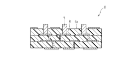
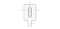
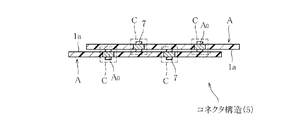
本発明の電気接続構造は、図1と図1のII−II線に沿う断面図である図2で1例として示したフレキシブル基板を第1の接続部材Aとし、その第1の接続部材Aの貫通孔4に、図3で1例として示した第2の接続部材Bの導電性突起7を挿入して組立てられ、例えば図7で示した断面構造になっている。
First, the basic form of the electrical connection structure of the present invention will be described.
In the electrical connection structure of the present invention, the flexible substrate shown as an example in FIG. 2 which is a cross-sectional view taken along line II-II in FIGS. 1 and 1 is used as the first connection member A, and the first connection member A. The
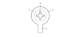
第1の接続部材Aはいわゆるフレキシブル基板であって、可撓性を有する薄い絶縁フィルム1と、その片面1aの所定箇所に形成された少なくとも1個(図1では3個)のパッド部2と、このパッド部2の縁部から引出されて所定のパターンで絶縁フィルム1の表面1aに配線された信号線の導電回路パターン3と、それぞれのパッド部2の面内位置において絶縁フィルム1の厚み方向に形成された貫通孔4と、それぞれのパッド部2の面内に形成され、貫通孔4と同軸的に連通していて、貫通孔4よりは小さい小孔5とで構成されている。なお、図1と図2で示したパッド部2の場合、貫通孔4の上端部にその一部が張り出した状態になっている。
The first connecting member A is a so-called flexible substrate, which is a thin
この第1の接続部材Aの基材である絶縁フィルム1としては、例えばポリイミド、ポリエステル、液晶ポリマ、ポリエーテルエーテルケトン(PEEK)などの樹脂から成るフィルム、薄いガラスエポキシ複合板やBTレジン基板などを用いることができる。
これら絶縁フィルムの厚みは、目的とする電気接続構造を低背化させることからすれば、機械的強度を損なわない範囲でできるだけ薄い方がよい。これら絶縁フィルムの市販品の最小の厚みは12.5μmであるが、上記した樹脂を適宜キャスティングや押出成形して10μm以下の厚みにして用いてもよい。
As the insulating
The thickness of these insulating films is preferably as thin as possible within a range that does not impair the mechanical strength in view of reducing the height of the intended electrical connection structure. The minimum thickness of commercially available insulating films is 12.5 μm, but the above-described resin may be cast or extruded as appropriate to have a thickness of 10 μm or less.
また、パッド部2を構成する材料としては、導電性と同時に弾力性を備えた材料であることが好ましい。この電気接続構造Aの場合、後述するように、このパッド部2の直下に形成される貫通孔4にパッド部2の形成面の方から第2の接続部材Bの導電性突起7を挿入したときに、導電性突起7の挿入方向に撓んだパッド部2がその復元力によって当該導電性突起7に圧接することによって2つの接続部材間の導通構造が形成されるので、このパッド部2は導電性を有することを必須の属性にするとともに弾力性が要求されるからである。このような材料としては、具体的には、銅、ニッケル、ステンレス鋼、リン青銅、インコネル(商標)などの金属や、樹脂に導電性の粉末が分散している導電性樹脂組成物などを好適例とする。
Moreover, as a material which comprises the
パッド部の厚みは格別限定されるものではないが、良好な弾力性を発揮させるためには、あまり厚くない方がよく、上限は100μm程度に制限すべきである。パッド部として銅のめっき層、スパッタリングで形成したニッケル薄膜、更にはこれらを組合せた導体層を用いた場合、厚みが0.05μm程度であっても、良好な導電性と弾力性を示すので好適である。 The thickness of the pad portion is not particularly limited, but in order to exhibit good elasticity, it is better not to be too thick, and the upper limit should be limited to about 100 μm. When a copper plating layer, a nickel thin film formed by sputtering, or a conductor layer that combines these is used as the pad portion, even if the thickness is about 0.05 μm, good conductivity and elasticity are preferable. It is.
図1で示した第1の接続部材Aを製造するに際しては、例えば片面銅張フィルムを用意し、その銅箔側の表面にフォトリソグラフィーとエッチング技術を適用して、パッド部2と導体回路パターン3の部分を残して他の銅箔部分をエッチング除去し、ついで、パット部2と反対側の表面から例えばレーザ光を照射してパッド部2の直下に貫通孔4を形成し、最後にパッド部2側の表面のうち小孔を形成すべき箇所以外をマスキングしたのち銅のエッチング処理を行なって貫通孔4と連通する小孔5を形成すればよい。化学エッチングやプラズマエッチングのプロセス技術を組合せれば、量産時の製造コストをはるかに低減することができる。
When the first connecting member A shown in FIG. 1 is manufactured, for example, a single-sided copper-clad film is prepared, and the
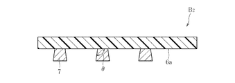
一方、第2の接続部材Bは、後述する電気・電子部品やプリント配線板などであって、その片面6aに形成された少なくとも1個(図3では3個)の導電性突起7と、この導電性突起7から引出されて所定のパターンで表面6aに配線された信号線の導体回路パターン8を備えている。
なお、この導電性突起7の配列パターンは、図1で示した第1の接続部材Aにおける貫通孔4の配列パターンと同じになっている。そして、これら導電性突起7の断面の大きさは、第1の接続部材Aの貫通孔4よりは小さく、小孔5よりは大きくなっている。また、この導体回路パターン8は第2の接続部材Bの表面6aに配線されずに、当該第2の接続部材Bの内部に埋設した状態で配線されていてもよい。
On the other hand, the second connection member B is an electric / electronic component or printed wiring board, which will be described later, and has at least one (three in FIG. 3)
The arrangement pattern of the
ここで、この第2の接続部材Bは第1の接続部材Aの相手材であって、例えば通常のリジッドなプリント配線板、各種の半導体モジュールや半導体素子、更には各種のセンサデバイスや表示デバイスなどである。また、第1の接続部材Aのようなフレキシブル基板であってもよい。
そして、これらのプリント配線板や電気・電子部品の所定表面に上記した導電性突起を形成することによって、この第2の接続部材Bが製造される。
Here, the second connecting member B is a mating member of the first connecting member A. For example, a normal rigid printed wiring board, various semiconductor modules and semiconductor elements, and various sensor devices and display devices. Etc. Moreover, a flexible substrate like the 1st connection member A may be sufficient.
And this 2nd connection member B is manufactured by forming the above-mentioned electroconductive protrusion on the predetermined surface of these printed wiring boards or an electrical / electronic component.
この導電性突起の形成に際しては、例えば第2の接続部材Bの表面に表出しているランド部や端子部に、通常のめっき処理や電鋳を選択的に行なうことによりその箇所に導電材料を堆積して所定形状の突起を形成すればよい。逆に、第2の接続部材Bの表面に厚く堆積した導電材料の層に部分的なエッチング処理を行なって形成することもできる。
また、ワイヤボンディング技術を活用して形成したスタッドバンプも実用に供することができる。更には、導電ペーストを第2の接続部材の表面にスクリーン印刷することによっても、必要箇所に導電性突起を形成することができる。
When forming the conductive protrusions, for example, a normal plating process or electroforming is selectively performed on the land portion or the terminal portion exposed on the surface of the second connection member B, so that a conductive material is applied to the portion. The protrusions having a predetermined shape may be formed by depositing. Conversely, the conductive material layer deposited thickly on the surface of the second connection member B may be formed by performing a partial etching process.
A stud bump formed by utilizing wire bonding technology can also be put to practical use. Furthermore, the conductive protrusion can be formed at a necessary location by screen-printing the conductive paste on the surface of the second connecting member.
そしてこれらの導電性突起は、第2の接続部材Bの表面6aに配線されている導体回路パターン8の上だけではなく、ビアホールの上などに形成することもできる。例えば第2の接続部材Bが薄い絶縁フィルムを基材とするフレキシブル基板である場合、図4で示したように、反対側の表面6bに形成した導体回路パターン8から絶縁フィルム1を貫通して表面6aに突出する導電性突起7を形成することができる。この構造にすると、製造した第2の接続部材Bにおける導電性突起7の機械的強度が高くなるので好適である。
These conductive protrusions can be formed not only on the
また、図5で示したように、絶縁フィルム1を基材とするフレキシブル基板の導体回路パターン8の所定箇所に導電性突起7を突設し、更にカバーレイ6cをかけた構造の場合も、導電性突起7の機械的強度の向上を実現することができる。
更に、図6で示したように、多層リジッドプリント配線板におけるある内層回路から最上層の表面6aに導電性突起7を突設した第2の接続部材の場合も同様の効果が得られる。
In addition, as shown in FIG. 5, in the case of a structure in which
Further, as shown in FIG. 6, the same effect can be obtained in the case of the second connecting member in which the
本発明の電気接続構造を組立てるに際しては、第2の接続部材Bの導電性突起7のそれぞれを、パッド部2の形成面側から小孔5を介して第1の接続部材Aのパッド部2のそれぞれの直下に位置する貫通孔4に挿入すればよい。
その結果、図7で示したように、導電性突起7はパッド部2の小孔5を貫通して貫通孔4の中に挿入される。そしてこの過程で貫通孔4の上端部に位置するパッド部の張り出し部分は拡径して撓み、同時に絶縁フィルムもパッド部2に同期して撓み、それらの弾性によってパッド部2の張り出し部分が導電性突起7の腹部と圧接する。その結果、導電性突起7とパッド部2の間、すなわち、第1の接続部材Aと第2の接続部材Bの間では電気的な接続構造Cが形成される。そして、一方の接続部材の導体回路パターンを伝播してきた信号は、この電気接続構造Cを介して他方の接続部材に伝搬する。
When assembling the electrical connection structure of the present invention, each of the
As a result, as shown in FIG. 7, the
このように、電気接続構造Cでは、図2で示したように、第1の接続部材Aに形成されている小孔5とパッド部2と貫通孔4で構成される箇所がメス端子部A0として機能し、また第2の接続部材Bに形成されている導電性突起7がオス端子部B0として機能する。
そして、この接続構造Cは、第1の接続部材Aのメス端子部A0におけるパッド部2と第2の接続部材Bの導電性突起7が機械的に接触した構造になっているので、第1の接続部材Aを第2の接続部材Bから引き剥せば、この接続構造Cを解除することができる。そのとき、パッド部2は材料の弾性によって撓んだ状態からもとの位置に復元し、再度、メス端子部A0としての使用が可能な状態に戻る。
In this way, in the electrical connection structure C, as shown in FIG. 2, the location formed by the
Then, the connection structure C, since the
本発明の電気接続構造において、その接続状態の信頼性、確実性を高めるために、第1の接続部材Aの前記したメス端子部A0と第2の接続部材Bの前記したオス端子部B0をそれぞれ次のような態様で形成しておくことが好ましい。
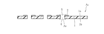
まず、図8で示した第1の接続部材A1のメス端子部A0の場合は、絶縁フィルム1の片面1aにパッド部2が形成され、そしてパッド部2に形成される小孔5と貫通孔4の平面視形状が同一になっている。
In the electrical connection structure of the present invention, the above-described female terminal portion A 0 of the first connection member A and the above-described male terminal portion B of the second connection member B in order to enhance the reliability and certainty of the connection state. It is preferable to form 0 in the following manner.
First, in the case of the female terminal portion A 0 of the first connecting member A 1 shown in FIG. 8, the
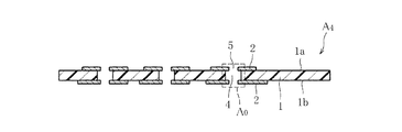
図9で示した第1の接続部材A2は、絶縁フィルム1の片面1aに形成されたパッド部2の小孔5が貫通孔4よりも小さくなっていて、パッド部2が貫通孔4の上端部に一部張り出している構造のメス端子部A0を有するものである。
図10で示した第1の接続部材A3は、絶縁フィルム1の他方の表面1bにもパッド部2が形成されていて、かつ小孔5と貫通孔4は同じ大きさになっている構造のメス端子部A0を有するものである。
In the first connecting member A 2 shown in FIG. 9, the
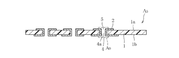
The first connecting member A 3 shown in FIG. 10 has a structure in which the
図11で示した第1の接続部材A4は、絶縁フィルムの他方の表面1bにもパッド部2が形成され、かつ、上下面のパッド部2,2のそれぞれは貫通孔4の上下端部に一部張り出している構造のメス端子部A0を有するものである。
そして図12で示した第1の接続部材A5は、絶縁フィルム1の上面1aと下面1bにもパッド部2,2が形成され、貫通孔4の壁面4aにも例えば貴金属の無電解めっきを施して2つのパッド部2,2間で導通をとっている構造のメス端子部A0を有するものである。そして小孔5と貫通孔4は同じ大きさになっている。
In the first connecting member A 4 shown in FIG. 11, the
The first connecting member A 5 shown in FIG. 12 has
これらの第1の接続部材において、例えば接続部材A3,A4のように、絶縁フィルム1の両面にパッド部2,2を形成したものは、メス端子部A0としての弾力性が高くなるので好適である。また、接続時の導電性の問題でいえば、接続部材A5のように貫通孔の壁面に耐食性の貴金属めっき処理を施したものが好適である。
なお、パッド部2に形成する小孔5の平面視形状は、後述するオス端子部B0である導電性突起7を挿入することができる形状であればよく、格別限定されるものではないが、例えば、図13で示したように、貫通孔4より小径の円形孔、図14で示したように、十文字形状をしたスリット孔、図15で示したように、円形孔と十文字スリット孔を組合せた孔、図16で示したように円形孔と三方スリット孔を組合わせた孔、図17で示したように、複数のスリット孔を中心を1つにして集合させた孔、図18で示したように、星型の孔、図19で示したように、平面視形状がムカデ形状をした孔などをあげることができる。
In these first connection members, for example, the connection members A 3 and A 4 in which the
Note that the plan view shape of the
これら小孔のうち、例えば図14や図15で示したスリット孔は、ここに第2の接続部材Bの導電性突起7を挿入したときに、スリット孔周辺の4個の舌片部が撓んでパット部が導電性突起に確実に圧接して接続構造の導通性の信頼を高めることができると同時に、挿抜を反復しても良好な接続構造を維持することができるという点で好適である。更に、スリット孔の数を増加したり、図19で示したように、導電性突起との接触部の長さを長くすることにより、接続の信頼性を高めることができる。
Among these small holes, for example, the slit holes shown in FIG. 14 and FIG. 15 have four tongue pieces bent around the slit hole when the
一方、第2の接続部材Bにおけるオス端子部B0を構成する導電性突起7の形状は、第1の接続部材Aのメス端子部A0に挿入されたときに、パッド部2と確実に接触して導通がとれる形状であればよく、格別限定されるものではない。
例えば、図20で示したように、表面6aに対する立ち上がり角度(θ)が90°である柱状体、図21で示したように立ち上がり角度(θ)が鈍角になっている突起、図22で示したように台座の上にそれよりも小径の柱状体を重ね合せたような突起、図23で示したように頂部が基部よりも大きくなっている柱状突起、図24で示したように、中央部がくびれている柱状突起などを例示することができる。
On the other hand, the shape of the
For example, as shown in FIG. 20, a columnar body whose rising angle (θ) is 90 ° relative to the
これらのうち、接続部材B2,B4,B5のように、頂部の断面形状が基部の断面形状よりも大きくなっている導電性突起は、これを第1の接続部材Aのメス端子部A0に挿入したときに、メス端子部A0のパッド部2に対してアンカー効果を発揮して抜脱しにくくなるので好適である。そして、接続部材B2のような突起を形成する場合には、立ち上がり角度(θ)を65〜160°の範囲に設定することが好ましい。
Among these, like the connection members B 2 , B 4 , and B 5 , the conductive projections whose top section has a larger cross-sectional shape than the base section have a female terminal portion of the first connection member A. when inserted into a 0, it is suitable because hardly pulled out by anchor effect with respect to the
表面6aを基点としたこれら導電性突起7の全体の高さは、70μm以上に設定することが好ましい。この高さが70μmより低い場合は、第1の接続部材Aのメス端子部A0に挿入されたとき、パッド部2との機械的接触を起こさなかったり、パッド部2との圧接状態が不充分になったりして、接続構造Cとしての接続信頼性が低下するからである。しかし、あまり高くすると、接続構造Cの低背化という目的を満たすことができなくなるので、最大でも700μm程度に規制すべきである。
The overall height of these
なお、これら導電性突起7の断面形状も格別限定されるものではないが、例えば、菱形、四角形、三角形、多角形、円形などの形状をあげることができる。
このような導電性突起7の材料としては、メス端子部A0への挿入時にパッド部2との間で摺動することになるので、耐摩耗性を確保するために、少なくともその表面が比較的硬質な金属または合金で構成されていることが好ましい。具体的には、銅、ニッケル、金、パラジウム、ロジウム、銀などをあげることができ、また例えば樹脂から成る軟質な芯体の表面に例えばニッケル、金、白金、ロジウム、パラジウム、銀、錫、はんだなどのめっき処理を施して表面だけを選択的に硬質化してもよい。逆に、カーボンや鉄などを含む導電性の塗料を塗布することも、信頼性を高める点で有効である。
In addition, although the cross-sectional shape of these
As a material of such a
なお、それぞれの接続部材におけるメス端子部A0とオス端子部B0(導電性突起7)の面内配列に関しては、格別限定されるものではないが、例えば第1の接続部材Aのメス端子部A0をマトリックス状に2次元配列し、また第2の接続部材Bのオス端子部B0を上記したメス端子部A0の配列に対応するマトリックス状に2次元配列すると、小さい平面スペース内に多数の接続点を有する接続構造Cを形成することができるので、接続部の省スペース化という点で好適である。 The in-plane arrangement of the female terminal portion A 0 and the male terminal portion B 0 (conductive protrusion 7) in each connection member is not particularly limited. For example, the female terminal of the first connection member A When the portion A 0 is two-dimensionally arranged in a matrix and the male terminal portion B 0 of the second connecting member B is two-dimensionally arranged in a matrix corresponding to the above-described arrangement of the female terminal A 0 , a small plane space is obtained. Since the connection structure C having a large number of connection points can be formed, it is preferable in terms of space saving of the connection part.
例えば、メス端子部A0の径をいずれも60μm、ピッチを200μmとし、100行100列の2次元配列にすれば、20mm角の平面スペース内に、10000点の接続点を有する接続構造Cの形成が可能になる。
上記した第1の接続部材Aと第2の接続部材Bをそれぞれ後述するように変形して本発明の電気接続構造を組立てることにより、多彩な機能を発揮する電気・電子装置を製作することができる。以下に、それを詳細に説明する。
(1)コネクタ構造
図7で示した本発明の電気接続構造Cが組込まれているコネクタ構造の1例を図25に示す。
For example, if the female terminal portion A 0 has a diameter of 60 μm, a pitch of 200 μm, and a two-dimensional array of 100 rows and 100 columns, the connection structure C having 10,000 connection points in a 20 mm square space Formation becomes possible.
It is possible to manufacture an electric / electronic device that exhibits various functions by assembling the electrical connection structure of the present invention by modifying the first connection member A and the second connection member B as described later. it can. This will be described in detail below.
(1) Connector structure FIG. 25 shows an example of a connector structure in which the electrical connection structure C of the present invention shown in FIG. 7 is incorporated.
図25のコネクタ構造(1)においては、第2の接続部材Bの片面6aに形成された所定パターンで配列する導電性突起(オス端子部B0)7を、第1の接続部材Aに形成され、貫通孔とパッド部と小孔から成るメス端子部A0に挿入して電気接続構造Cが形成されている。
例えば、導電性突起(オス端子部B0)7は、直径0.15mm、高さ0.15mmで、ピッチ間隔を0.5mmにして、6行10列のマトリックス状に配列されている。一方、第1の接続部材Aには、直径0.125mmの貫通孔、直径0.25mmのパッド部、このパッド部の中心に直径0.1mmの小孔が形成されてメス端子部A0が導電性突起の場合と同じマトリックスの配列で形成されている。その場合、オス端子部B0とメス端子部A0で形成された60ピンの接続構造Cの形状は、縦6.0mm、横4.0mm、高さ0.3mmであり、占有面積は24mm2であり、全体の体積は7.2mm3であった。
In the connector structure (1) of FIG. 25, conductive protrusions (male terminal portions B 0 ) 7 arranged in a predetermined pattern formed on one
For example, the conductive protrusions (male terminal portions B 0 ) 7 are arranged in a matrix of 6 rows and 10 columns with a diameter of 0.15 mm, a height of 0.15 mm, and a pitch interval of 0.5 mm. On the other hand, the first connecting member A has a through hole having a diameter of 0.125 mm, a pad portion having a diameter of 0.25 mm, and a small hole having a diameter of 0.1 mm formed at the center of the pad portion, so that the female terminal portion A 0 is formed. It is formed with the same matrix arrangement as in the case of the conductive protrusions. In that case, the shape of the 60-pin connection structure C formed by the male terminal portion B 0 and the female terminal portion A 0 is 6.0 mm in length, 4.0 mm in width, 0.3 mm in height, and occupies an area of 24 mm. 2 and the total volume was 7.2 mm 3 .
なお、実際の接続作業においては、このコネクタ構造(1)は狭ピッチ多ピンであるにもかかわらず、容易にメス接続部A0とオス接続部B0の位置合わせができ、オス接続部B0のメス接続部A0への挿入操作を円滑に行なうことができた。そして脱着作業も何の障害もなく円滑に行なえた。また、反復して挿抜することも容易であった。
一方、オスコネクタとメスコネクタを機械的に噛み合せた従来の60ピンコネクタ構造の場合、接続部の最小サイズは、縦3.5mm、横21mm、高さ1mm程度であり、占有面積は73.5mm2であり、全体の体積は73.5mm3である。
In actual connection work, the female connector A 0 and the male connector B 0 can be easily aligned even though this connector structure (1) is a narrow-pitch, multi-pin connector. the operation of inserting into the female connection portion a 0 of 0 could be performed smoothly. And the desorption work could be done smoothly without any obstacles. Moreover, it was easy to repeatedly insert and remove.
On the other hand, in the case of a conventional 60-pin connector structure in which a male connector and a female connector are mechanically engaged, the minimum size of the connecting portion is 3.5 mm in length, 21 mm in width, and about 1 mm in height, and the occupied area is 73.5 mm . 2 and the total volume is 73.5 mm 3 .
以上のことから明らかなように、本発明の電気接続構造Cを組込んだコネクタ構造(1)の場合、挿抜作業を円滑に行なうことができ、加えて従来の最小サイズのコネクタ構造に比べて大幅な低背化を実現しており、かつ省スペース化も実現している。
また、このコネクタ構造(1)における接続構造Cの信頼性評価試験を行なった。
(a)接続部の接触抵抗に及ぼす挿抜回数の影響
コネクタ構造(1)の挿抜操作を反復し、その都度、13個の接続点につき接続部の接触抵抗を測定した。その結果を13点の平均値として図26に示した。
As is clear from the above, in the case of the connector structure (1) incorporating the electrical connection structure C of the present invention, the insertion / extraction operation can be performed smoothly, and in addition to the conventional minimum size connector structure. It has achieved a significant reduction in profile and space saving.
Moreover, the reliability evaluation test of the connection structure C in this connector structure (1) was conducted.
(A) Influence of the number of insertions and removals on the contact resistance of the connection part The insertion / extraction operation of the connector structure (1) was repeated, and each time the contact resistance of the connection part was measured at 13 connection points. The results are shown in FIG. 26 as an average value of 13 points.
図26から明らかなように、接触抵抗は0.05Ω以下と非常に小さく、200回の挿抜操作を反復しても、接触抵抗はほとんど増大しておらず、良好な導電性が確保されている。
(b)接続部の保持力に及ぼす挿抜回数の影響
コネクタ構造(1)の挿抜操作を反復し、その都度、接続部を解除するために必要な力(接続部の保持力)を測定した。その結果を図27に示した。
As is clear from FIG. 26, the contact resistance is very small, 0.05Ω or less, and even after 200 insertion / extraction operations, the contact resistance hardly increases and good conductivity is ensured. .
(B) Influence of the number of insertions and removals on the holding force of the connection part The insertion / extraction operation of the connector structure (1) was repeated, and each time the force necessary to release the connection part (holding force of the connection part) was measured. The results are shown in FIG.
図27から明らかなように、最初の数10回の挿抜操作の反復では、接続部の保持力は若干低下するが、やがて安定化し、その後の挿抜操作を反復してもほとんど変化しておらず、信頼性の高い接続構造になっているといえる。
なお、接続部の保持力の初期段階における低下現象は、メス端子部とオス端子部がなじむための安定化プロセスであると考えられる。
(c)接続部の耐熱試験
コネクタ構造(1)を、温度120℃の環境下に保持したのち取り出して接続部の接触抵抗を測定した。その結果を、保持時間との関係図として図28に示した。
As is clear from FIG. 27, the holding force of the connection portion is slightly reduced in the first tens of repetitions of the insertion / extraction operation, but eventually stabilizes and hardly changes even when the subsequent insertion / extraction operation is repeated. It can be said that it has a highly reliable connection structure.
In addition, it is thought that the fall phenomenon in the initial stage of the retention strength of a connection part is the stabilization process for a female terminal part and a male terminal part to adjust.
(C) Heat resistance test of connecting portion The connector structure (1) was held in an environment at a temperature of 120 ° C and then taken out to measure the contact resistance of the connecting portion. The results are shown in FIG. 28 as a relationship diagram with the retention time.
図28から明らかなように、温度120℃の環境に100時間保持しても、接続部の接触抵抗はほとんど変化しておらず、このコネクタ構造(1)は熱的に安定であることが判明した。
以上の試験結果から明らかなように、本発明の接続構造Cは、接触抵抗が小さく、挿抜操作を反復しても接触抵抗の増加がなく、また熱的にも安定であり、高い信頼性を備えている。
As is clear from FIG. 28, the contact resistance of the connecting portion hardly changed even when kept in an environment of 120 ° C. for 100 hours, and it was found that this connector structure (1) was thermally stable. did.
As is clear from the above test results, the connection structure C of the present invention has a small contact resistance, does not increase the contact resistance even when the insertion / extraction operation is repeated, is thermally stable, and has high reliability. I have.
図29は別のコネクタ構造(2)を示す。
このコネクタ構造(2)の場合は、表面6aに形成された導電性突起7に加えて、表面6aと反対側の表面6bにも導電性突起7が形成されている第2の接続部材Bを用い、これら両面の導電性突起7のそれぞれを2枚の第1の接続部材Aのメス端子部A0に挿入して、本発明の電気接続構造Cが形成されている。
FIG. 29 shows another connector structure (2).
In the case of this connector structure (2), in addition to the
このコネクタ構造(2)では、第2の接続部材Bがオス型のインターポーザとして機能している。
図30は更に別のコネクタ構造(3)を示す。
このコネクタ構造(3)では、1枚の第1の接続部材Aのメス端子部A0に2枚の第2の接続部材Bの導電性突起7を第1の接続部材Aの上面と下面からそれぞれ挿入して本発明の電気接続構造Cが形成されている。
In this connector structure (2), the second connecting member B functions as a male interposer.
FIG. 30 shows still another connector structure (3).
In the connector structure (3), the one first connecting member and the second connecting member
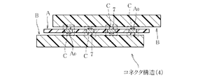
図31は別のコネクタ構造(4)を示す。
このコネクタ構造(4)は、図30のコネクタ構造(3)の変形例であるが、ここでは、第1の接続部材Aがメス型のインターポーザとして機能している。
図32に他のコネクタ構造(5)を示す。
このコネクタ構造(5)は、第1の接続部材Aを変形したフレキシブル基板を2枚用いて組立てられる。すなわち、第1の接続部材Aにおいてパッド部が位置する表面1aに導電性突起7が形成され、それぞれの導電性突起7を他方の第1の接続部材Aのメス端子部A0に挿入して本発明の電気接続構造Cが形成されている。
FIG. 31 shows another connector structure (4).
This connector structure (4) is a modification of the connector structure (3) of FIG. 30, but here, the first connecting member A functions as a female interposer.
FIG. 32 shows another connector structure (5).
This connector structure (5) is assembled by using two flexible boards obtained by deforming the first connecting member A. That is, the pad portion in the first connecting member A is formed
この場合、それぞれの導電性突起7とメス端子部A0を縦横交互に千鳥状に配列しておくと、組立てられた接続構造Cにおける接続の信頼性を高めることができて好適である。
以上のコネクタ構造において、第1の接続部材Aのメス端子部を構成する貫通孔(とパッド部)をマトリックス状に配列し、また相手材である第2の接続部材Bの導電性突起も、上記したマトリックスに対応して配列しておくと、形成した接続構造Cが占有する平面スペースを大幅に小さくすることができ、省スペースの点で好適である。
In this case, when the respective
In the above connector structure, the through holes (and the pad portions) constituting the female terminal portion of the first connection member A are arranged in a matrix, and the conductive protrusions of the second connection member B which is the mating member are also Arranging in correspondence with the above-described matrix can significantly reduce the plane space occupied by the formed connection structure C, which is preferable in terms of space saving.
なお、上記したコネクタ構造を解除する場合は、例えばフレキシブル基板である第1の接続部材Aを手動で引き剥がせばよい。
(2)フィルムケーブル構造
本発明の電気接続構造Cが組込まれているフィルムケーブル構造の1例を図33に示す。
In addition, what is necessary is just to peel off the 1st connection member A which is a flexible substrate manually, for example, when canceling | releasing the above-mentioned connector structure.
(2) Film cable structure FIG. 33 shows an example of a film cable structure in which the electrical connection structure C of the present invention is incorporated.
このフィルムケーブル構造の場合、所定の配列パターンでメス端子部A0が形成され、同時に表面1aに同じ配列パターンで導電性突起7が形成されている複数(図33では3枚)の第1の接続部材A(長尺なフレキシブル基板)の各メス端子部A0に別の第1の接続部材Aの導電性突起(オス端子部B0)を挿入して本発明の電気接続構造Cを形成することにより、各フレキシブル基板を長手方向に連結してケーブルにしている。
In the case of this film cable structure, a plurality of (three in FIG. 33) first projections in which the female terminal portion A 0 is formed in a predetermined arrangement pattern and at the same time the
このケーブルにおける各接続部は低背であり、ケーブル全体としては極めて薄く可撓性である。また、いずれかの接続部材が断線した場合、ただちに手動で接続構造Cを解除し、そこにあらたな接続部材Aを接続してケーブルを復元することができる。
(3)その他の組立て構造体
表面に所定の回路パターンが配線されている回路基板に、本発明の電気接続構造Cを有する電子部品が表面実装された構造体の1例を図34に示す。
Each connection portion in this cable has a low profile, and the entire cable is extremely thin and flexible. Moreover, when any one of the connection members is disconnected, the connection structure C can be immediately released manually, and a new connection member A can be connected there to restore the cable.
(3) Other Assembly Structure FIG. 34 shows an example of a structure in which an electronic component having the electrical connection structure C of the present invention is surface-mounted on a circuit board on which a predetermined circuit pattern is wired.
図34の構造体の場合、第2の接続部材Bとして、導電性突起7が形成されている表面6aと反対側の表面6bに例えばはんだバンプ電極8が形成されているものが用いられる。
そして、この第2の接続部材Bの導電性突起7を第1の接続部材Aであるフレキシブル基板のメス端子部A0に挿入して本発明の電気接続構造Cが形成されている。そして、第2の接続部材Bのはんだバンプ電極8が、回路基板9のランド部9aに例えばリフロー処理によって接合されて、電気接続構造Cを含む部品が表面実装されている。
In the case of the structure shown in FIG. 34, as the second connection member B, one in which, for example, the
Then, and it is electrically connected structure C is formed of the present invention by inserting the
この構造体の場合、低背化した接続構造Cを実現することができ、しかも例えばメス端子部A0と導電性突起7の配列をマトリックス状に2次元化すれば、接続部の大幅な省スペース化を実現することができる。したがって、回路基板9への表面実装作業に余裕が生まれ、また従来に比べて多くの部品実装が可能となる。そして、第1の接続部材Aは着脱自在であるため、その第1の接続部材Aとして、それぞれが各種の機能を発揮するフィルム回路基板を用いることにより、この構造体に必要に応じて各種の機能を発揮させることができる。
In the case of this structure, the connection structure C with a reduced height can be realized, and if the arrangement of the female terminal portions A0 and the
図35は、図34で示した第2の接続部材Bに代えてフレキシブル基板である第1の接続部材Aを用いて組立てた構造体の1例を示す。
この構造体では、パッド部とは反対側の表面1bに例えばはんだバンプ電極8が形成された第1の接続部材Aが用いられている。そして片面に導電性突起7が形成されているフレキシブル基板を第2の接続部材Bとし、その導電性突起7を第1の接続部材Aのメス端子部A0に挿入して本発明の電気接続構造Cが形成され、その全体ははんだバンプ電極8を介して回路基板9のランド部9aに表面実装されている。
FIG. 35 shows an example of a structure assembled using the first connection member A, which is a flexible substrate, instead of the second connection member B shown in FIG.
In this structure, a first connection member A in which, for example, a
図36は、本発明の電気接続構造Cを介してICチップが表面実装された構造体の1例を示す。
この構造体では、第2の接続部材BとしてICチップ10が用いられる。そして第1の接続部材Aとしては、図35の場合と同様に、パッド部とは反対側の表面1bに例えばはんだバンプ電極8が形成されている第1の接続部材Aであるフレキシブル基板が用いられる。
FIG. 36 shows an example of a structure in which an IC chip is surface-mounted through the electrical connection structure C of the present invention.
In this structure, the
ICチップ10の片面の例えばランド部には、既に説明した第2の接続部材Bにおける導電性突起7が形成されていて、この導電性突起7を第1の接続部材Aのメス端子部A0に挿入して本発明の電気接続構造Cが形成されている。そして全体は、はんだバンプ電極8を介して回路基板9のランド部9aに表面実装されている。
この構造体の場合、ICチップ10は着脱自在の状態にあるため、例えばICチップ10が故障した場合にはそれを取り外し、導電性突起が取りつけられた新たなICチップで代替することができる。
The
In the case of this structure, since the
図37は、本発明の電気接続構造Cが組込まれている多層回路基板構造体(図では3層回路基板)の1例を示す。
この構造体は、3枚の第1の接続部材(フレキシブル基板)Aを用いて組立てられている。それぞれの接続部材Aには所定の回路パターン1cが配線されていて、それ自体がフレキシブルな回路基板になっている。そして、図示した2枚の接続部材A(上層の2枚)の場合は、それぞれの回路パターン1cと電気的に接続して導電性突起7が形成されている。しかし、図示の構造体では、最下層の接続部材Aに導電性突起は形成されていない。
FIG. 37 shows an example of a multilayer circuit board structure (three-layer circuit board in the figure) in which the electrical connection structure C of the present invention is incorporated.
This structure is assembled using three first connection members (flexible substrates) A. Each connection member A is provided with a
そしてこの構造体は、各接続部材Aの導電性突起7を下層に位置する接続部材Aのメス端子部A0に挿入して本発明の電気接続構造Cを形成することにより、各接続部材Aを順次積層して組立てられている。
この構造体は、薄い各第1の接続部材Aを単位基板とし、それを機械的に積層して製作した多層回路基板である。図では3層構造を示したが、同様の構造の第1の接続部材Aを用いてそれらを順次積層することにより、更なる層数の多層回路基板に組立てることができる。
And this structure, by forming an electrical connection structure C of the insert to the present invention the female terminal portions A 0 of the connecting member A for positioning the
This structure is a multilayer circuit board manufactured by mechanically laminating each thin first connecting member A as a unit board. Although a three-layer structure is shown in the figure, it is possible to assemble a multilayer circuit board having a further number of layers by sequentially laminating them using the first connection member A having a similar structure.
また、各単位基板(第1の接続部材)は着脱自在な状態になっているので、ある単位基板に支障が生じた場合でも、簡単にそれを新しい単位基板と代替することができる。
図38は、本発明の電気接続構造Cが組込まれたスタックドパッケージ構造体の1例を示す。
この構造体は、次のようなフレキシブル基板を用いて組立てられる。すなわち、図39で示したように、絶縁フィルム1として、その周縁部1dにパッド部を含めたメス端子部A0および/または導電性突起7が形成され、絶縁フィルム1の中央部1eには半導体素子の実装領域が形成されているフレキシブル基板が用いられる。そして、図39の仮想線で示したように、この中央部1eに所定の半導体素子11が表面実装されている。
In addition, since each unit substrate (first connecting member) is detachable, even when a certain unit substrate is troubled, it can be easily replaced with a new unit substrate.
FIG. 38 shows an example of a stacked package structure in which the electrical connection structure C of the present invention is incorporated.
This structure is assembled using the following flexible substrate. That is, as shown in FIG. 39, as the insulating
図38で示した構造体は、半導体素子11が表面実装された図39のフレキシブル基板(第1の接続部材)Aの導電性突起7を下層に位置するフレキシブル基板Aのメス端子部A0に挿入して本発明の電気接続構造Cを順次形成し、各フレキシブル基板Aを積層して組立てられる。
この構造体は、各基板それ自体が薄く、また各接続部が低背化しているので、全体としても非常に薄くなっており、また接続部のメス端子部A0とオス端子部(導電性突起)7の配列をマトリックス状に2次元化することにより省スペース化も実現することができる。
Structure shown in FIG. 38, the female terminal portion A 0 of the flexible substrate A for positioning the flexible substrate (first connecting member)
In this structure, each substrate itself is thin and each connection portion is low-profile, so that the overall structure is very thin. Also, the female terminal portion A 0 and the male terminal portion (conductivity) of the connection portion. Space saving can also be realized by two-dimensionally arranging the
そして、各層の半導体素子11が故障した場合であっても、それが実装されているフレキシブル基板Aのみを取り外し、新規な基板に取り替えることができる。
図40は、本発明の電気接続構造Cにおける第2の接続部材Bの1例を示す。
この接続部材Bは、基材としてフレキシブル基板が用いられ、その片面6aに導電性突起7がマトリックス状に配列されている。そして、片面6aの4隅には、柱状ガイド12a,12aと穴付柱状ガイド12b,12bが配設されている。
And even if it is a case where the
FIG. 40 shows an example of the second connection member B in the electrical connection structure C of the present invention.
The connecting member B uses a flexible substrate as a base material, and
この接続部材の相手材である第1の接続部材(図示しない)には、前記マトリックス状の導電性突起と対応する位置に既に説明したメス端子部が形成されていると同時に、上記した柱状ガイドと穴付き柱状ガイドに対応する表面位置には、これらガイドを受け入れるメス型のガイドが形成されている。
そして、接続構造の組立てに際しては、接続部材Bの上記した柱状ガイド12a,12aと穴付き柱状ガイド12b,12bを相手材である第1の接続部材のメス型ガイドに嵌合したのち、全体を押圧して導電性突起7を第1の接続部材のメス端子部に挿入して目的とする接続構造にする。
In the first connecting member (not shown) which is the mating member of the connecting member, the female terminal portion already described is formed at a position corresponding to the matrix-shaped conductive protrusion, and at the same time, the above columnar guide A female guide for receiving these guides is formed at the surface position corresponding to the columnar guide with holes.
When assembling the connection structure, after fitting the above-mentioned
このように、この接続部材Bにおける柱状ガイドや穴付き柱状ガイドを設けることにより、導電性突起とメス端子部の位置合わせを円滑に進めることができる。とくに、接続構造の組立てを自動化で行なう場合には、接続部材Bにこのような柱状ガイドや穴付き柱状ガイドを設けておくことが好適である。
図41は、第2の接続部材の他の例を示す。
Thus, by providing the columnar guide or the columnar guide with a hole in the connection member B, the alignment of the conductive protrusion and the female terminal portion can be smoothly advanced. In particular, when the assembly of the connection structure is performed automatically, it is preferable to provide such a column guide or a column guide with a hole in the connection member B.
FIG. 41 shows another example of the second connection member.
この接続部材は、図40で示した接続部材における柱状ガイドや穴付き柱状ガイドに代えて、マトリックス状に配列されている導電性突起7を取り囲んで配設されたガイドウォール13を備えている。そして、相手材である第1の接続部材には、このガイドウォール13を受け入れる凹溝が形成されている。
このガイドウォール13も、接続構造の組立て時に、各接続部材の位置合わせを円滑に進める手段として機能する。
This connecting member is provided with a
This
A,A1,A2,A3,A4,A5 第1の接続部材
A0 メス端子部
B,B1,B2,B3,B4,B5, 第2の接続部材
B0 オス端子部
C 電気接続構造
1 絶縁フィルム
1a 絶縁フィルム1の片面
1b 絶縁フィルム1の他方の表面
1c 回路パターン
1d 絶縁フィルム1の周縁部
1e 絶縁フィルム1の中央部
2 パッド部
3 導電回路パターン
4 貫通孔
5 小孔
6a 第2の接続部材Bの表面
6b 第2の接続部材Bの反対側の表面
6c カバーレイ
7 導電性突起
8 導電回路パターン
9 回路基板
9a ランド部
10 ICチップ
11 半導体素子
12a 柱状ガイド
12b 穴付柱状ガイド
13 ガイドウォール
A, A 1 , A 2 , A 3 , A 4 , A 5 1st connecting member A 0 female terminal part
B, B 1 , B 2 , B 3 , B 4 , B 5 , second connecting member B 0 male terminal portion C
Claims (13)
内部または表面に形成された導体回路パターンと電気的に接続する導電性突起が外部に表出して形成されている第2の接続部材とを組付けて構成される電気接続部材であって、
前記第2の接続部材の前記導電性突起が前記第1の接続部材の前記貫通孔に前記パッド部の形成面側から前記小孔を介して挿入され、
前記パッド部とそれが形成されている箇所の前記絶縁フィルムが前記導電性突起の挿入方向に撓み、前記パッド部と前記絶縁フィルムの弾性により、前記パッド部が前記導電性突起に圧接されていることを特徴とする電気接続構造。A flexible insulating film; a conductive pad portion formed on the surface of the insulating film; a conductor circuit pattern drawn from an edge of the pad portion; A first connecting member that is a flexible substrate including a through hole formed in the thickness direction of the insulating film, and a small hole that is coaxially connected to the through hole and formed in the surface of the pad portion ;
Conductive projections for connecting internal or electrically to the conductor circuit pattern formed on the surface of an electrical connection member constituted by assembling a second connection member which is formed by exposed to the outside,
The conductive protrusion of the second connection member is inserted into the through hole of the first connection member from the formation surface side of the pad portion through the small hole,
The pad part and the insulating film where the pad part is formed are bent in the insertion direction of the conductive protrusion, and the pad part is pressed against the conductive protrusion by the elasticity of the pad part and the insulating film . An electrical connection structure characterized by that.
Applications Claiming Priority (1)
| Application Number | Priority Date | Filing Date | Title |
|---|---|---|---|
| PCT/JP2006/321534 WO2008050448A1 (en) | 2006-10-27 | 2006-10-27 | Electrical connection structure |
Publications (2)
| Publication Number | Publication Date |
|---|---|
| JP4059522B1 true JP4059522B1 (en) | 2008-03-12 |
| JPWO2008050448A1 JPWO2008050448A1 (en) | 2010-02-25 |
Family
ID=39243674
Family Applications (1)
| Application Number | Title | Priority Date | Filing Date |
|---|---|---|---|
| JP2007513583A Active JP4059522B1 (en) | 2006-10-27 | 2006-10-27 | Electrical connection structure and first connection member used therefor |
Country Status (6)
| Country | Link |
|---|---|
| US (1) | US7785113B2 (en) |
| EP (1) | EP2117082B1 (en) |
| JP (1) | JP4059522B1 (en) |
| CN (1) | CN101273494B (en) |
| TW (1) | TW200838384A (en) |
| WO (1) | WO2008050448A1 (en) |
Cited By (13)
| Publication number | Priority date | Publication date | Assignee | Title |
|---|---|---|---|---|
| WO2009139323A1 (en) * | 2008-05-15 | 2009-11-19 | 株式会社旭電化研究所 | Connector structure |
| WO2010047141A1 (en) * | 2008-10-21 | 2010-04-29 | 株式会社旭電化研究所 | Female connector, male connector assembled thereto, and electric/electronic apparatus using the connectors |
| EP2345314A1 (en) * | 2008-10-18 | 2011-07-20 | Conti Temic Microelectronic GmbH | Flexible printed circuit board |
| US8192207B2 (en) | 2010-02-26 | 2012-06-05 | Panasonic Corporation | Female circuit board having non-circular conduction portions and conformal to insertion portions |
| WO2014002592A1 (en) * | 2012-06-29 | 2014-01-03 | 株式会社 村田製作所 | Structure for affixing cable to wiring board, cable, and method for manufacturing cable |
| JP2014017155A (en) * | 2012-07-10 | 2014-01-30 | Panasonic Corp | Connector device |
| US8708712B2 (en) | 2009-12-25 | 2014-04-29 | Panasonic Corporation | Male connector block, female connector block, and connector |
| JP2014519694A (en) * | 2011-06-16 | 2014-08-14 | バリアン・メディカル・システムズ・インコーポレイテッド | Electron emitting device for X-ray tube |
| US9466905B2 (en) | 2012-10-29 | 2016-10-11 | Asahi Denka Kenkyusho Co., Ltd. | Connector structure, female connector, and male connector |
| US9478879B2 (en) | 2012-07-10 | 2016-10-25 | Panasonic Intellectual Property Management Co., Ltd. | Connector assembly and female connector used for the same |
| JP2019193093A (en) * | 2018-04-24 | 2019-10-31 | 株式会社日立製作所 | Ultrasonic sending/receiving element, and ultrasonic inspection device, smart phone and tablet including the same |
| JP2020184694A (en) * | 2019-05-08 | 2020-11-12 | 株式会社日立製作所 | Ultrasonic probe and ultrasonic transmitter/receiver using the same |
| CN113411953A (en) * | 2021-06-17 | 2021-09-17 | 深圳佑驾创新科技有限公司 | Printed circuit board and packaging structure thereof |
Families Citing this family (50)
| Publication number | Priority date | Publication date | Assignee | Title |
|---|---|---|---|---|
| JP5175489B2 (en) * | 2007-04-27 | 2013-04-03 | 新光電気工業株式会社 | Manufacturing method of semiconductor package |
| WO2010086956A1 (en) * | 2009-01-27 | 2010-08-05 | エヌワイ工業株式会社 | Connection structure of flexible substrate and opponent member |
| DE102010010331A1 (en) * | 2010-03-04 | 2011-09-08 | Phoenix Contact Gmbh & Co. Kg | Electrical contact arrangement |
| US8215966B2 (en) * | 2010-04-20 | 2012-07-10 | Tyco Electronics Corporation | Interposer connector assembly |
| JP5702081B2 (en) * | 2010-06-10 | 2015-04-15 | 株式会社旭電化研究所 | Pseudo coaxial flat cable and plug structure |
| JP5609451B2 (en) * | 2010-09-09 | 2014-10-22 | 富士通株式会社 | Connector, optical transmission device and connector connection method |
| JP5570395B2 (en) * | 2010-10-08 | 2014-08-13 | モレックス インコーポレイテド | Sheet connector |
| US8569167B2 (en) | 2011-03-29 | 2013-10-29 | Micron Technology, Inc. | Methods for forming a semiconductor structure |
| GB201119045D0 (en) | 2011-11-04 | 2011-12-14 | Rolls Royce Plc | Electrical harness |
| GB201119050D0 (en) * | 2011-11-04 | 2011-12-14 | Rolls Royce Plc | Electrical harness connector |
| GB2498006B (en) * | 2011-12-22 | 2014-07-09 | Rolls Royce Plc | Gas turbine engine systems |
| JP2013218237A (en) | 2012-04-12 | 2013-10-24 | Japan Display Inc | Liquid crystal display device |
| JP5907503B2 (en) * | 2012-08-30 | 2016-04-26 | アルプス電気株式会社 | Electronics |
| JP2014063975A (en) * | 2012-08-31 | 2014-04-10 | Nidec Copal Corp | Flexible printed wiring board and apparatus equipped with the same |
| TWI460945B (en) * | 2012-09-07 | 2014-11-11 | Chief Land Electronic Co Ltd | Method and structure of solder terminal hung with solder and connector therof |
| KR101722140B1 (en) * | 2012-09-21 | 2017-03-31 | 엘에스엠트론 주식회사 | Electrical connector assembly, electrical connector assembly for board-to-board and board-to-cable including same |
| US8834182B2 (en) * | 2012-10-17 | 2014-09-16 | Microelectronics Assembly Technologies | Pierced flexible circuit and compression joint |
| US20140104776A1 (en) * | 2012-10-17 | 2014-04-17 | James E. Clayton | Rigid circuit board with flexibly attached module |
| CN103889148B (en) * | 2012-12-21 | 2017-03-15 | 上海天马微电子有限公司 | A kind of flexible PCB and manufacture method, display module |
| US9039448B2 (en) | 2013-02-18 | 2015-05-26 | Tyco Electronics Corporation | Electronic interconnect devices having conductive vias |
| KR102038102B1 (en) * | 2013-03-07 | 2019-10-30 | 삼성디스플레이 주식회사 | Resistance measuring apparatus for inspecting compression quality and measuring method using the same |
| US9374898B2 (en) * | 2013-04-24 | 2016-06-21 | Apple Inc. | Electrical and mechanical interconnection for electronic components |
| GB201308028D0 (en) | 2013-05-03 | 2013-06-12 | Rolls Royce Plc | Electrical harness connector |
| GB201308029D0 (en) | 2013-05-03 | 2013-06-12 | Rolls Royce Plc | Electrical harness connector |
| US9723725B2 (en) * | 2013-05-29 | 2017-08-01 | Finisar Corporation | Rigid-flexible circuit interconnects |
| KR101488266B1 (en) * | 2013-08-06 | 2015-01-30 | 주식회사 유니드 | Matable electrical interconnection structure for electrical interconnection, connector, semiconductor package assembly, and electrical device having the same |
| US9105288B1 (en) | 2014-03-11 | 2015-08-11 | Magnecomp Corporation | Formed electrical contact pad for use in a dual stage actuated suspension |
| DE102014103895A1 (en) * | 2014-03-21 | 2015-09-24 | Bender & Wirth Gmbh & Co. | Interconnects |
| US9748723B2 (en) * | 2014-12-12 | 2017-08-29 | Peter Sussman | Solder-less board-to-wire connector |
| JP6665979B2 (en) * | 2015-05-19 | 2020-03-13 | 日本電子材料株式会社 | Electrical contact |
| US10008797B2 (en) | 2015-07-10 | 2018-06-26 | Te Connectivity Corporation | Flexible printed circuit connector and connector assembly including the same |
| EP3357310B1 (en) * | 2015-09-28 | 2021-06-23 | Tactotek Oy | Multilayer structure and related method of manufacture for electronics |
| JP6748517B2 (en) | 2016-08-25 | 2020-09-02 | 日本航空電子工業株式会社 | Connector assembly |
| DE102016223194B4 (en) * | 2016-11-23 | 2018-07-26 | Robert Bosch Gmbh | Battery cell comprising at least one galvanic cell, battery and method for producing a battery cell |
| DE102016223187B3 (en) * | 2016-11-23 | 2018-03-22 | Robert Bosch Gmbh | A battery comprising a first battery cell and a second battery cell and a method of electrically contacting a first battery cell with a second battery cell for assembling a battery |
| KR102421623B1 (en) * | 2016-12-01 | 2022-07-19 | 쓰리엠 이노베이티브 프로퍼티즈 컴파니 | Electronic device comprising a flexible component layer having an interlocking device |
| DE102016225973B4 (en) * | 2016-12-22 | 2019-06-13 | Conti Temic Microelectronic Gmbh | Method for contacting a contact surface on a flexible printed circuit board with a metal contact, connection of flexible printed circuit board and metal contact and control unit |
| KR101944997B1 (en) * | 2017-01-06 | 2019-02-01 | 조인셋 주식회사 | Metal pad interface |
| CN210443547U (en) * | 2017-03-31 | 2020-05-01 | 株式会社村田制作所 | Electronic device |
| US10133133B1 (en) * | 2017-06-28 | 2018-11-20 | Advanced Optoelectronic Technology, Inc | Liquid crystal display base |
| EP3435490B1 (en) * | 2017-07-24 | 2019-11-20 | Japan Aviation Electronics Industry, Ltd. | Connection assisting member and circuit board assembly |
| CN109524822A (en) * | 2017-09-20 | 2019-03-26 | 泰科电子(上海)有限公司 | Conductive terminal and connector |
| US10998160B2 (en) * | 2018-08-21 | 2021-05-04 | General Electric Company | Cathode emitter to emitter attachment system and method |
| US11245215B2 (en) * | 2018-11-20 | 2022-02-08 | Samsung Display Co., Ltd. | Connector for display device |
| KR102306042B1 (en) * | 2018-12-11 | 2021-09-27 | 주식회사 엘지에너지솔루션 | FPCB assembly for battery module and a method for manufacturing FPCB assembly and a battery module including the same |
| JP7144332B2 (en) * | 2019-01-21 | 2022-09-29 | 日本航空電子工業株式会社 | Connector, wiring board assembly and connection structure |
| JP2021027177A (en) * | 2019-08-05 | 2021-02-22 | 日立オートモティブシステムズ株式会社 | Circuit board |
| US11121489B2 (en) * | 2019-08-20 | 2021-09-14 | Seagate Technology Llc | Electrical connector with flexible circuit and stiffener |
| CN112449488A (en) * | 2019-09-05 | 2021-03-05 | 华为技术有限公司 | Circuit board and electronic equipment |
| CN113677103A (en) * | 2021-08-24 | 2021-11-19 | 无锡胜脉电子有限公司 | Welding structure for ceramic packaging pressure sensor |
Family Cites Families (55)
| Publication number | Priority date | Publication date | Assignee | Title |
|---|---|---|---|---|
| US3077511A (en) * | 1960-03-11 | 1963-02-12 | Int Resistance Co | Printed circuit unit |
| US3214827A (en) * | 1962-12-10 | 1965-11-02 | Sperry Rand Corp | Electrical circuitry fabrication |
| US3541223A (en) * | 1966-09-23 | 1970-11-17 | Texas Instruments Inc | Interconnections between layers of a multilayer printed circuit board |
| US3541225A (en) * | 1968-12-20 | 1970-11-17 | Gen Electric | Electrical conductor with improved solder characteristics |
| US3795047A (en) * | 1972-06-15 | 1974-03-05 | Ibm | Electrical interconnect structuring for laminate assemblies and fabricating methods therefor |
| US3859711A (en) * | 1973-03-20 | 1975-01-14 | Ibm | Method of detecting misregistration of internal layers of a multilayer printed circuit panel |
| US4394712A (en) * | 1981-03-18 | 1983-07-19 | General Electric Company | Alignment-enhancing feed-through conductors for stackable silicon-on-sapphire wafers |
| US4511757A (en) * | 1983-07-13 | 1985-04-16 | At&T Technologies, Inc. | Circuit board fabrication leading to increased capacity |
| US4720470A (en) * | 1983-12-15 | 1988-01-19 | Laserpath Corporation | Method of making electrical circuitry |
| JPS63246837A (en) | 1987-04-02 | 1988-10-13 | Canon Inc | Electric circuit member |
| US5502889A (en) * | 1988-06-10 | 1996-04-02 | Sheldahl, Inc. | Method for electrically and mechanically connecting at least two conductive layers |
| US4929185A (en) * | 1989-04-03 | 1990-05-29 | Nrc Corporation | Printed circuit board assembly |
| US5030110A (en) * | 1989-11-06 | 1991-07-09 | Litton Systems, Inc. | Case assembly for stacking integrated circuit packages |
| US5132879A (en) * | 1990-10-01 | 1992-07-21 | Hewlett-Packard Company | Secondary board for mounting of components having differing bonding requirements |
| US5128831A (en) * | 1991-10-31 | 1992-07-07 | Micron Technology, Inc. | High-density electronic package comprising stacked sub-modules which are electrically interconnected by solder-filled vias |
| US5282312A (en) * | 1991-12-31 | 1994-02-01 | Tessera, Inc. | Multi-layer circuit construction methods with customization features |
| US5199879A (en) * | 1992-02-24 | 1993-04-06 | International Business Machines Corporation | Electrical assembly with flexible circuit |
| US5617300A (en) * | 1993-08-23 | 1997-04-01 | Nagano Japan Radio Co., Ltd. | Connecting method of printed substrate and apparatus |
| JP2867209B2 (en) * | 1993-08-27 | 1999-03-08 | 日東電工株式会社 | Method of connecting flexible circuit board to contact object and structure thereof |
| US5610371A (en) * | 1994-03-15 | 1997-03-11 | Fujitsu Limited | Electrical connecting device and method for making same |
| CA2135241C (en) | 1993-12-17 | 1998-08-04 | Mohi Sobhani | Cavity and bump interconnection structure for electronic packages |
| US5456004A (en) * | 1994-01-04 | 1995-10-10 | Dell Usa, L.P. | Anisotropic interconnect methodology for cost effective manufacture of high density printed circuit boards |
| US5414223A (en) * | 1994-08-10 | 1995-05-09 | Ast Research, Inc. | Solder pad for printed circuit boards |
| CA2157259C (en) * | 1994-08-31 | 2000-08-29 | Koetsu Tamura | Electronic device assembly and a manufacturing method of the same |
| US5938455A (en) * | 1996-05-15 | 1999-08-17 | Ford Motor Company | Three-dimensional molded circuit board having interlocking connections |
| US5825633A (en) * | 1996-11-05 | 1998-10-20 | Motorola, Inc. | Multi-board electronic assembly including spacer for multiple electrical interconnections |
| US6188028B1 (en) | 1997-06-09 | 2001-02-13 | Tessera, Inc. | Multilayer structure with interlocking protrusions |
| CA2213590C (en) * | 1997-08-21 | 2006-11-07 | Keith C. Carroll | Flexible circuit connector and method of making same |
| US6086384A (en) * | 1997-08-22 | 2000-07-11 | Molex Incorporated | Method of fabricating electronic device employing a flat flexible circuit and including the device itself |
| US5873740A (en) * | 1998-01-07 | 1999-02-23 | International Business Machines Corporation | Electrical connector system with member having layers of different durometer elastomeric materials |
| US6030234A (en) * | 1998-01-23 | 2000-02-29 | Molex Incorporated | Terminal pins mounted in flexible substrates |
| US5951305A (en) * | 1998-07-09 | 1999-09-14 | Tessera, Inc. | Lidless socket and method of making same |
| EP0982978B1 (en) * | 1998-08-25 | 2005-05-25 | Kiekert Aktiengesellschaft | Housing, in particular lock housing with electrical interconnections |
| US6354000B1 (en) * | 1999-05-12 | 2002-03-12 | Microconnex Corp. | Method of creating an electrical interconnect device bearing an array of electrical contact pads |
| US6524115B1 (en) * | 1999-08-20 | 2003-02-25 | 3M Innovative Properties Company | Compliant interconnect assembly |
| JP2001076787A (en) | 1999-09-03 | 2001-03-23 | Shin Etsu Polymer Co Ltd | Electric connector and connection structure using it |
| US6490168B1 (en) * | 1999-09-27 | 2002-12-03 | Motorola, Inc. | Interconnection of circuit substrates on different planes in electronic module |
| US6347042B1 (en) * | 1999-10-26 | 2002-02-12 | International Business Machines Corporation | Printed circuit board top side mounting standoff |
| JP3694825B2 (en) * | 1999-11-18 | 2005-09-14 | 日本航空電子工業株式会社 | Conductive pattern forming method and connector, flexible printed wiring board, anisotropic conductive member |
| DE19957789A1 (en) * | 1999-12-01 | 2001-06-21 | Leoni Bordnetz Sys Gmbh & Co | Contact system for two circuit boards |
| US6200146B1 (en) * | 2000-02-23 | 2001-03-13 | Itt Manufacturing Enterprises, Inc. | Right angle connector |
| US6326698B1 (en) * | 2000-06-08 | 2001-12-04 | Micron Technology, Inc. | Semiconductor devices having protective layers thereon through which contact pads are exposed and stereolithographic methods of fabricating such semiconductor devices |
| US6456506B1 (en) * | 2000-06-23 | 2002-09-24 | Chiang Chun Lin | Electronic retainer for preventing electromagnetic interference and capable of being absorbed mechanically |
| JP3897278B2 (en) * | 2001-04-05 | 2007-03-22 | カシオマイクロニクス株式会社 | Manufacturing method of flexible wiring board |
| KR100484168B1 (en) * | 2002-10-11 | 2005-04-19 | 삼성전자주식회사 | Ink jet printhead and manufacturing method thereof |
| US6921860B2 (en) * | 2003-03-18 | 2005-07-26 | Micron Technology, Inc. | Microelectronic component assemblies having exposed contacts |
| US7088008B2 (en) * | 2003-03-20 | 2006-08-08 | International Business Machines Corporation | Electronic package with optimized circuitization pattern |
| US6817870B1 (en) | 2003-06-12 | 2004-11-16 | Nortel Networks Limited | Technique for interconnecting multilayer circuit boards |
| US6881074B1 (en) * | 2003-09-29 | 2005-04-19 | Cookson Electronics, Inc. | Electrical circuit assembly with micro-socket |
| US6966784B2 (en) * | 2003-12-19 | 2005-11-22 | Palo Alto Research Center Incorporated | Flexible cable interconnect assembly |
| US7119276B2 (en) * | 2004-07-09 | 2006-10-10 | Dell Products L.P. | Method and apparatus for board mounting in a chassis |
| JP2006156943A (en) * | 2004-09-28 | 2006-06-15 | Seiko Epson Corp | Wiring pattern forming method, wiring pattern, and electronic equipment |
| US7541826B2 (en) * | 2005-05-13 | 2009-06-02 | Kla-Tencor Corporation | Compliant pad wafer chuck |
| JP2007087679A (en) * | 2005-09-21 | 2007-04-05 | Alps Electric Co Ltd | Connecting element |
| US7448923B2 (en) * | 2006-09-14 | 2008-11-11 | Harshad K Uka | Connection for flex circuit and rigid circuit board |
-
2006
- 2006-10-27 US US11/885,262 patent/US7785113B2/en active Active
- 2006-10-27 JP JP2007513583A patent/JP4059522B1/en active Active
- 2006-10-27 WO PCT/JP2006/321534 patent/WO2008050448A1/en active Application Filing
- 2006-10-27 EP EP06822495.5A patent/EP2117082B1/en active Active
- 2006-10-27 CN CN2006800067096A patent/CN101273494B/en active Active
-
2007
- 2007-03-01 TW TW096107010A patent/TW200838384A/en unknown
Cited By (24)
| Publication number | Priority date | Publication date | Assignee | Title |
|---|---|---|---|---|
| WO2009139323A1 (en) * | 2008-05-15 | 2009-11-19 | 株式会社旭電化研究所 | Connector structure |
| KR101166343B1 (en) | 2008-05-15 | 2012-07-18 | 가부시키가이샤 아사히 덴카 겐큐쇼 | Connector structure, female connector and male connector used therein, flexible circuit board, rigid circuit board, and electric and electronic equipiment incorporating connector structure |
| US8267700B2 (en) | 2008-05-15 | 2012-09-18 | Asahi Denka Kenkyusho Co., Ltd. | Connector structure |
| EP2345314A1 (en) * | 2008-10-18 | 2011-07-20 | Conti Temic Microelectronic GmbH | Flexible printed circuit board |
| WO2010047141A1 (en) * | 2008-10-21 | 2010-04-29 | 株式会社旭電化研究所 | Female connector, male connector assembled thereto, and electric/electronic apparatus using the connectors |
| US8215965B2 (en) | 2008-10-21 | 2012-07-10 | Asahi Denka Kenkyusho Co., Ltd. | Female connector, male connector assembled to the same, and electric/electronic apparatus using them |
| JP5373809B2 (en) * | 2008-10-21 | 2013-12-18 | 株式会社旭電化研究所 | Female connector, male connector to be assembled to it, and electrical / electronic equipment using them |
| US8708712B2 (en) | 2009-12-25 | 2014-04-29 | Panasonic Corporation | Male connector block, female connector block, and connector |
| US8192207B2 (en) | 2010-02-26 | 2012-06-05 | Panasonic Corporation | Female circuit board having non-circular conduction portions and conformal to insertion portions |
| JP2014519694A (en) * | 2011-06-16 | 2014-08-14 | バリアン・メディカル・システムズ・インコーポレイテッド | Electron emitting device for X-ray tube |
| US9647312B2 (en) | 2012-06-29 | 2017-05-09 | Murata Manufacturing Co., Ltd. | Fixing structure of cable to wiring substrate, and cable, and manufacturing method of cable |
| WO2014002592A1 (en) * | 2012-06-29 | 2014-01-03 | 株式会社 村田製作所 | Structure for affixing cable to wiring board, cable, and method for manufacturing cable |
| JPWO2014002592A1 (en) * | 2012-06-29 | 2016-05-30 | 株式会社村田製作所 | Fixing structure or fixing method of cable to circuit board |
| JP5900766B2 (en) * | 2012-06-29 | 2016-04-06 | 株式会社村田製作所 | Fixing structure or fixing method of cable to circuit board |
| US9077127B2 (en) | 2012-07-10 | 2015-07-07 | Panasonic Intellectual Property Management Co., Ltd. | Connector assembly |
| US9478879B2 (en) | 2012-07-10 | 2016-10-25 | Panasonic Intellectual Property Management Co., Ltd. | Connector assembly and female connector used for the same |
| JP2014017155A (en) * | 2012-07-10 | 2014-01-30 | Panasonic Corp | Connector device |
| US9466905B2 (en) | 2012-10-29 | 2016-10-11 | Asahi Denka Kenkyusho Co., Ltd. | Connector structure, female connector, and male connector |
| JP2019193093A (en) * | 2018-04-24 | 2019-10-31 | 株式会社日立製作所 | Ultrasonic sending/receiving element, and ultrasonic inspection device, smart phone and tablet including the same |
| JP7079648B2 (en) | 2018-04-24 | 2022-06-02 | 富士フイルムヘルスケア株式会社 | Manufacturing method of ultrasonic probe, ultrasonic probe, ultrasonic inspection device, smartphone, and tablet |
| JP2020184694A (en) * | 2019-05-08 | 2020-11-12 | 株式会社日立製作所 | Ultrasonic probe and ultrasonic transmitter/receiver using the same |
| JP7236320B2 (en) | 2019-05-08 | 2023-03-09 | 富士フイルムヘルスケア株式会社 | Ultrasonic probe and ultrasonic transmitter/receiver using the same |
| CN113411953A (en) * | 2021-06-17 | 2021-09-17 | 深圳佑驾创新科技有限公司 | Printed circuit board and packaging structure thereof |
| CN113411953B (en) * | 2021-06-17 | 2022-06-10 | 深圳佑驾创新科技有限公司 | Printed circuit board and packaging structure thereof |
Also Published As
| Publication number | Publication date |
|---|---|
| CN101273494B (en) | 2012-02-22 |
| EP2117082A4 (en) | 2012-05-16 |
| US20090233465A1 (en) | 2009-09-17 |
| EP2117082A1 (en) | 2009-11-11 |
| JPWO2008050448A1 (en) | 2010-02-25 |
| CN101273494A (en) | 2008-09-24 |
| WO2008050448A1 (en) | 2008-05-02 |
| TW200838384A (en) | 2008-09-16 |
| US7785113B2 (en) | 2010-08-31 |
| TWI342175B (en) | 2011-05-11 |
| EP2117082B1 (en) | 2016-05-18 |
Similar Documents
| Publication | Publication Date | Title |
|---|---|---|
| JP4059522B1 (en) | Electrical connection structure and first connection member used therefor | |
| JP4584144B2 (en) | Circuit board device and wiring board connection method | |
| JP5373809B2 (en) | Female connector, male connector to be assembled to it, and electrical / electronic equipment using them | |
| US7238044B2 (en) | Connection structure of printed wiring board | |
| JP5274584B2 (en) | Connection structure between flexible board and mating member | |
| WO2004098252A1 (en) | Printed wiring board connection structure | |
| JP2007207618A (en) | Narrow pitch flexible wiring | |
| EP2913897B1 (en) | Connector structure, female connector and male connector | |
| JP4210049B2 (en) | Spiral contact | |
| KR100885121B1 (en) | Electrical connection structure | |
| JP3640268B2 (en) | Connector and connector manufacturing method | |
| JP2010114326A (en) | Flexible printed wiring board | |
| WO2012011193A1 (en) | Connection structure between flexible substrate and partner member | |
| JP4172433B2 (en) | Substrate connecting member, three-dimensional connecting structure using the same, and manufacturing method of three-dimensional connecting structure | |
| JP2010287606A (en) | Flexible printed wiring board, and connector structure integrated with flexible printed wiring board | |
| JP2008218185A (en) | Anisotropic conductive member and device connection structure using this | |
| JP2008182178A (en) | Connection pin, and connection structure of printed board | |
| JP2006313759A (en) | Spiral contactor |
Legal Events
| Date | Code | Title | Description |
|---|---|---|---|
| TRDD | Decision of grant or rejection written | ||
| A01 | Written decision to grant a patent or to grant a registration (utility model) |
Free format text: JAPANESE INTERMEDIATE CODE: A01 Effective date: 20071212 |
|
| A61 | First payment of annual fees (during grant procedure) |
Free format text: JAPANESE INTERMEDIATE CODE: A61 Effective date: 20071217 |
|
| FPAY | Renewal fee payment (event date is renewal date of database) |
Free format text: PAYMENT UNTIL: 20101228 Year of fee payment: 3 |
|
| R150 | Certificate of patent or registration of utility model |
Free format text: JAPANESE INTERMEDIATE CODE: R150 Ref document number: 4059522 Country of ref document: JP Free format text: JAPANESE INTERMEDIATE CODE: R150 |
|
| FPAY | Renewal fee payment (event date is renewal date of database) |
Free format text: PAYMENT UNTIL: 20101228 Year of fee payment: 3 |
|
| FPAY | Renewal fee payment (event date is renewal date of database) |
Free format text: PAYMENT UNTIL: 20121228 Year of fee payment: 5 |
|
| R250 | Receipt of annual fees |
Free format text: JAPANESE INTERMEDIATE CODE: R250 |
|
| FPAY | Renewal fee payment (event date is renewal date of database) |
Free format text: PAYMENT UNTIL: 20131228 Year of fee payment: 6 |
|
| R250 | Receipt of annual fees |
Free format text: JAPANESE INTERMEDIATE CODE: R250 |
|
| R250 | Receipt of annual fees |
Free format text: JAPANESE INTERMEDIATE CODE: R250 |
|
| R250 | Receipt of annual fees |
Free format text: JAPANESE INTERMEDIATE CODE: R250 |
|
| R250 | Receipt of annual fees |
Free format text: JAPANESE INTERMEDIATE CODE: R250 |
|
| R250 | Receipt of annual fees |
Free format text: JAPANESE INTERMEDIATE CODE: R250 |
|
| R250 | Receipt of annual fees |
Free format text: JAPANESE INTERMEDIATE CODE: R250 |
|
| R250 | Receipt of annual fees |
Free format text: JAPANESE INTERMEDIATE CODE: R250 |
|
| R250 | Receipt of annual fees |
Free format text: JAPANESE INTERMEDIATE CODE: R250 |
|
| R250 | Receipt of annual fees |
Free format text: JAPANESE INTERMEDIATE CODE: R250 |
|
| R250 | Receipt of annual fees |
Free format text: JAPANESE INTERMEDIATE CODE: R250 |