EP1487024A1 - Lateral junctiion field-effect transistor and its manufacturing method - Google Patents
Lateral junctiion field-effect transistor and its manufacturing method Download PDFInfo
- Publication number
- EP1487024A1 EP1487024A1 EP02786001A EP02786001A EP1487024A1 EP 1487024 A1 EP1487024 A1 EP 1487024A1 EP 02786001 A EP02786001 A EP 02786001A EP 02786001 A EP02786001 A EP 02786001A EP 1487024 A1 EP1487024 A1 EP 1487024A1
- Authority
- EP
- European Patent Office
- Prior art keywords
- semiconductor layer
- gate electrode
- doped
- layer
- impurities
- Prior art date
- Legal status (The legal status is an assumption and is not a legal conclusion. Google has not performed a legal analysis and makes no representation as to the accuracy of the status listed.)
- Withdrawn
Links
Images















Classifications
-
- H—ELECTRICITY
- H10—SEMICONDUCTOR DEVICES; ELECTRIC SOLID-STATE DEVICES NOT OTHERWISE PROVIDED FOR
- H10D—INORGANIC ELECTRIC SEMICONDUCTOR DEVICES
- H10D30/00—Field-effect transistors [FET]
- H10D30/01—Manufacture or treatment
- H10D30/051—Manufacture or treatment of FETs having PN junction gates
-
- H—ELECTRICITY
- H10—SEMICONDUCTOR DEVICES; ELECTRIC SOLID-STATE DEVICES NOT OTHERWISE PROVIDED FOR
- H10D—INORGANIC ELECTRIC SEMICONDUCTOR DEVICES
- H10D30/00—Field-effect transistors [FET]
- H10D30/80—FETs having rectifying junction gate electrodes
- H10D30/83—FETs having PN junction gate electrodes
-
- H—ELECTRICITY
- H10—SEMICONDUCTOR DEVICES; ELECTRIC SOLID-STATE DEVICES NOT OTHERWISE PROVIDED FOR
- H10D—INORGANIC ELECTRIC SEMICONDUCTOR DEVICES
- H10D62/00—Semiconductor bodies, or regions thereof, of devices having potential barriers
- H10D62/01—Manufacture or treatment
- H10D62/051—Forming charge compensation regions, e.g. superjunctions
-
- H—ELECTRICITY
- H10—SEMICONDUCTOR DEVICES; ELECTRIC SOLID-STATE DEVICES NOT OTHERWISE PROVIDED FOR
- H10D—INORGANIC ELECTRIC SEMICONDUCTOR DEVICES
- H10D62/00—Semiconductor bodies, or regions thereof, of devices having potential barriers
- H10D62/10—Shapes, relative sizes or dispositions of the regions of the semiconductor bodies; Shapes of the semiconductor bodies
- H10D62/102—Constructional design considerations for preventing surface leakage or controlling electric field concentration
- H10D62/103—Constructional design considerations for preventing surface leakage or controlling electric field concentration for increasing or controlling the breakdown voltage of reverse-biased devices
- H10D62/105—Constructional design considerations for preventing surface leakage or controlling electric field concentration for increasing or controlling the breakdown voltage of reverse-biased devices by having particular doping profiles, shapes or arrangements of PN junctions; by having supplementary regions, e.g. junction termination extension [JTE]
- H10D62/109—Reduced surface field [RESURF] PN junction structures
- H10D62/111—Multiple RESURF structures, e.g. double RESURF or 3D-RESURF structures
-
- H—ELECTRICITY
- H10—SEMICONDUCTOR DEVICES; ELECTRIC SOLID-STATE DEVICES NOT OTHERWISE PROVIDED FOR
- H10D—INORGANIC ELECTRIC SEMICONDUCTOR DEVICES
- H10D62/00—Semiconductor bodies, or regions thereof, of devices having potential barriers
- H10D62/10—Shapes, relative sizes or dispositions of the regions of the semiconductor bodies; Shapes of the semiconductor bodies
- H10D62/17—Semiconductor regions connected to electrodes not carrying current to be rectified, amplified or switched, e.g. channel regions
- H10D62/213—Channel regions of field-effect devices
- H10D62/221—Channel regions of field-effect devices of FETs
- H10D62/328—Channel regions of field-effect devices of FETs having PN junction gates
-
- H—ELECTRICITY
- H10—SEMICONDUCTOR DEVICES; ELECTRIC SOLID-STATE DEVICES NOT OTHERWISE PROVIDED FOR
- H10D—INORGANIC ELECTRIC SEMICONDUCTOR DEVICES
- H10D62/00—Semiconductor bodies, or regions thereof, of devices having potential barriers
- H10D62/10—Shapes, relative sizes or dispositions of the regions of the semiconductor bodies; Shapes of the semiconductor bodies
- H10D62/17—Semiconductor regions connected to electrodes not carrying current to be rectified, amplified or switched, e.g. channel regions
- H10D62/343—Gate regions of field-effect devices having PN junction gates
-
- H—ELECTRICITY
- H10—SEMICONDUCTOR DEVICES; ELECTRIC SOLID-STATE DEVICES NOT OTHERWISE PROVIDED FOR
- H10D—INORGANIC ELECTRIC SEMICONDUCTOR DEVICES
- H10D64/00—Electrodes of devices having potential barriers
- H10D64/20—Electrodes characterised by their shapes, relative sizes or dispositions
- H10D64/27—Electrodes not carrying the current to be rectified, amplified, oscillated or switched, e.g. gates
- H10D64/311—Gate electrodes for field-effect devices
- H10D64/411—Gate electrodes for field-effect devices for FETs
Definitions
- the present invention relates to a lateral junction field effect transistor, and particularly to a structure of a lateral junction field effect transistor, of which on-resistance can be reduced while maintaining good breakdown voltage properties, as well as a method of manufacturing the same.
- a gate electrode applies a reverse bias voltage to a pn junction located on a side of a channel region, through which carriers pass, so that a depletion layer stretches from the pn junction into the channel region.
- a conductance of the channel region is controlled to perform operations such as switching.
- the lateral JFET is configured to move the carriers parallel to an element surface in the channel region.
- the carriers in the channel may be either electrons (n-type) or holes (p-type).
- the JFET having a semiconductor substrate made of SiC usually employs a channel region formed of an n-type impurity region in many cases. For the sake of illustration, therefore, it is assumed in the following description that carriers in a channel are electrons, and thus a channel region is formed of an n-type impurity region. Naturally, the channel region may be formed of a p-type impurity region.
- Fig. 72 is a cross section showing a conventional lateral JFET (U.S. Patent No. 5,264,713, "Junction Field Effect Transistor in Silicon Carbide").
- a p + -type epitaxial layer 112 is arranged on an n-type SiC substrate 110, and an n-type channel layer 114 is arranged on epitaxial layer 112.
- an n + -type source region 116 and an n + -type drain region 118 are arranged, respectively.
- Source and drain electrodes 120 and 122 are arranged on source and drain regions 116 and 118, respectively.
- a gate contact layer 130 is formed on a rear surface of SiC substrate 110, and a gate electrode (not shown) is arranged on gate contact layer 130.
- Trench 124 located between source/drain regions 116 and 118 extends into channel layer 114.
- a channel C is formed in a portion of epitaxial layer 114 of a second conductivity type located between trench 124 and epitaxial layer 112 of the first conductivity type.
- Epitaxial layer 112 is doped with p-type impurities more heavily than epitaxial layer 114 including the channel and doped with n-type impurities, and therefore is configured such that the reverse bias voltage applied to the junction portion enlarges the depletion layer toward the channel.
- a magnitude of the reverse bias voltage can be controlled to fill the channel region with the depletion layer filling, and not to fill it.
- the space In the normally-off type, the space must be smaller than a space for the depletion layer extended by a diffused potential in a junction between channel layer 114 and gate contact layer 130, and therefore can be increased only to a limited extent so that the on-resistance can be lowered only to a limited extent.
- An object of the invention is to provide a lateral junction field effect transistor having a structure, which can reduce an on-resistance while maintaining good breakdown voltage properties.
- a lateral junction field effect transistor includes a first semiconductor layer located on a semiconductor substrate, and doped with impurities of a first conductivity type; a second semiconductor layer located on the first semiconductor layer, and doped with impurities of a second conductivity type more heavily than the first semiconductor layer; a third semiconductor layer located on the second semiconductor layer, and doped with impurities of the first conductivity type; a fourth semiconductor layer located on the third semiconductor layer, and doped with impurities of the second conductivity type; a fifth semiconductor layer located on the fourth semiconductor layer, and doped with impurities of the first conductivity type; source/drain region layers formed in the fifth semiconductor layer, spaced from each other by a predetermined distance, having a lower surface extending on the second semiconductor layer, and doped with impurities of the second conductivity type more heavily than the second and fourth semiconductor layers; a first gate electrode layer arranged in the third semiconductor layer between the source/drain region layers, having a lower surface extending on the second
- a method of manufacturing a lateral junction field effect transistor includes the steps of forming a first semiconductor layer doped with impurities of a first conductivity type on a semiconductor substrate; forming a second semiconductor layer doped with impurities of a second conductivity type more heavily than the first semiconductor layer on the first semiconductor layer; forming a third semiconductor layer doped with impurities of the first conductivity type on the second semiconductor layer; forming a first gate electrode layer located in the second and third semiconductor layers, and doped with impurities of the first conductivity type more heavily than the second semiconductor layer by implanting the impurities into a predetermined region of the third semiconductor layer; forming a fourth semiconductor layer doped with impurities of the second conductivity type on the third semiconductor layer; forming a fifth semiconductor layer doped with impurities of the first conductivity type on the fourth semiconductor layer; implanting impurities into a predetermined region of the fifth semiconductor layer to form a second gate electrode layer having a lower surface extending on the fourth semiconductor layer, having substantially the same im
- the transistor structures are formed in a vertical direction, i.e., in the same direction as the layering or stacking direction of the respective semiconductor layers on the semiconductor substrate. Therefore, an on-resistance of the element can be reduced, as compared with conventional structures.
- the second, third, fourth and fifth semiconductor layers substantially have the same impurity concentration and the same layer thickness.
- This structure can minimize the on-resistance of the lateral junction field effect transistor, and can maximize a value of a breakdown voltage.
- a distance between a top of the first semiconductor layer and a bottom of the first gate electrode layer is smaller than a distance of a depletion layer extended by a diffused potential in a junction between the second semiconductor layer and the first gate electrode layer, and a distance between a top of the third semiconductor layer and a bottom of the second gate electrode layer is smaller than a distance of a depletion layer extended by a diffused potential in a junction between the fourth semiconductor layer and the second gate electrode layer.
- one or more unit transistor structure(s) being substantially the same as the structure having the second semiconductor layer, the third semiconductor layer and the first gate electrode layer are arranged between the third and fourth semiconductor layers. According to this structure, three or more unit transistors can be stacked in the lateral junction field effect transistor.
- a lateral junction field effect transistor includes a first semiconductor layer located on a semiconductor substrate, and doped with impurities of a first conductivity type; a second semiconductor layer located on the first semiconductor layer, and doped with impurities of a second conductivity type more heavily than the first semiconductor layer; a third semiconductor layer located on the second semiconductor layer, and doped with impurities of the first conductivity type; a fourth semiconductor layer located on the third semiconductor layer, and doped with impurities of the second conductivity type; a fifth semiconductor layer located on the fourth semiconductor layer, and doped with impurities of the first conductivity type; source/drain region layers formed in the fifth semiconductor layer, spaced from each other by a predetermined distance, having a lower surface extending on the second semiconductor layer, and doped with impurities of the second conductivity type more heavily than the second and fourth semiconductor layers; a first gate electrode layer arranged in the third semiconductor layer between the source/drain region layers, having a lower surface extending on
- a method of manufacturing a lateral junction field effect transistor includes the steps of forming a first semiconductor layer doped with impurities of a first conductivity type on a semiconductor substrate; forming a second semiconductor layer doped with impurities of a second conductivity type more heavily than the first semiconductor layer on the first semiconductor layer; forming a first impurity doped region of the first conductivity type in the second semiconductor layer by implanting the impurities into a predetermined region of the second semiconductor layer; forming a third semiconductor layer doped with impurities of the first conductivity type on the second semiconductor layer; forming a first gate electrode layer located in the second and third semiconductor layers, and doped with impurities of the first conductivity type more heavily than the second semiconductor layer by implanting the impurities; forming a fourth semiconductor layer doped with impurities of the second conductivity type on the third semiconductor layer; implanting impurities into a predetermined region of the fourth semiconductor layer to form a second impurity doped region located in the fourth semiconductor layer, having substantially the
- the transistor structures are formed in a vertical direction, i.e., in the same direction as the stacking direction of the respective semiconductor layers on the semiconductor substrate. Therefore, the on-resistance of the element can be reduced, as compared with conventional structures.
- the second, third, fourth and fifth semiconductor layers substantially have the same impurity concentration and the same layer thickness.
- This structure can minimize the on-resistance of the lateral junction field effect transistor, and can maximize the value of the breakdown voltage.
- a distance between a top of the first semiconductor layer and a bottom of the first impurity doped region is smaller than a distance of a depletion layer extended by a diffused potential in a junction between the second semiconductor layer and the first impurity doped region
- a distance between a top of the first impurity doped region and a bottom of the first gate electrode layer is smaller than double a distance of a depletion layer extended by a diffused potential in a junction between the second semiconductor layer and the first gate electrode layer
- a distance between a top of the third semiconductor layer and a bottom of the second impurity doped region is smaller than double a distance of a depletion layer extended by a diffused potential in a junction between the fourth semiconductor layer and the second impurity doped region
- a distance between a top of the second impurity doped region and a bottom of the second gate electrode layer is smaller than double a distance of a depletion layer extended by a diffused potential in a junction
- the second semiconductor layer is provided with a plurality of layers of the first impurity doped regions
- the fourth semiconductor layer is provided with a plurality of layers of the second impurity doped. regions.
- the second and fourth semiconductor layers can be utilized to the maximum extent, and thereby it is possible to achieve the normally-off type of the lateral junction field effect transistor, in which a total channel width is increased and the on-resistance is lowered.
- one or more unit transistor structure(s) being substantially the same as the structure having the second semiconductor layer, the third semiconductor layer, the first gate electrode layer and the first impurity doped region are arranged between the third and fourth semiconductor layers. According to this structure, three o:r more unit transistors can be stacked in the lateral junction field effect transistor.
- a lateral junction field effect transistor includes a first semiconductor layer located on a semiconductor substrate, and doped with impurities of a first conductivity type; a second semiconductor layer located on the first semiconductor layer, and doped with impurities of a second conductivity type more heavily than the first semiconductor layer; a third semiconductor layer located on the second semiconductor layer, and doped with impurities of the first conductivity type; a fourth semiconductor layer located on the third semiconductor layer, and doped with impurities of the second conductivity type; a fifth semiconductor layer located on the fourth semiconductor layer, and doped with impurities of the first conductivity type; source/drain region layers formed in the fifth semiconductor layer, spaced from each other by a predetermined distance, having a lower surface extending on the second semiconductor layer, and doped with impurities of the second conductivity type more heavily than the second and fourth semiconductor layers; a first gate electrode layer arranged in the third semiconductor layer between the source/drain region layers, having a lower surface extending
- a method of manufacturing a lateral junction field effect transistor includes the steps of forming a first semiconductor layer doped with impurities of a first conductivity type on a semiconductor substrate; forming a second semiconductor layer doped with impurities of a second conductivity type more heavily than the first semiconductor layer on the first semiconductor layer; forming a third semiconductor layer doped with impurities of the first conductivity type on the second semiconductor layer; forming a fourth semiconductor layer doped with impurities of the second conductivity type on the third semiconductor layer; implanting impurities into a predetermined region of the fourth semiconductor layer to form a first gate electrode layer having a lower surface extending on the second semiconductor layer, having an upper surface extending on the fourth semiconductor layer, and doped with impurities of the first conductivity type more heavily than the second and fourth semiconductor layers; forming a fifth semiconductor layer doped with impurities of the first conductivity type on the fourth semiconductor layer; implanting impurities into a predetermined region of the fifth semiconductor layer to form a second gate electrode layer having
- the transistor structures are formed in a vertical direction, i.e., in the same direction as the stacking direction of the respective semiconductor layers on the semiconductor substrate. Therefore, the on-resistance of the element can be reduced, as compared with conventional structures.
- the second, third, fourth and fifth semiconductor layers substantially have the same impurity concentration and the same layer thickness.
- This structure can minimize the on-resistance of the lateral junction field effect transistor, and can maximize the value of the breakdown voltage.
- a distance between a top of the first semiconductor layer and a bottom of the first gate electrode layer is smaller than a distance of a depletion layer extended by a diffused potential in a junction between the second semiconductor layer and the first gate electrode layer, and a distance between a top of the first gate electrode layer and a bottom of the second gate electrode layer is smaller than double a distance of a depletion layer extended by a diffused potential in a junction between the fourth semiconductor layer and the first gate electrode layer.
- one or more unit transistor structure(s) being substantially the same as the structure having the third semiconductor layer, the fourth semiconductor layer and the first gate electrode layer are arranged between the fourth and fifth semiconductor layers. According to this structure, three or more unit transistors can be stacked in the lateral junction field effect transistor.
- a lateral junction field effect transistor includes a first semiconductor layer located on a semiconductor substrate, and doped with impurities of a first conductivity type; a second semiconductor layer located on the :first semiconductor layer, and doped with impurities of a second conductivity type more heavily than the first semiconductor layer; a third semiconductor layer located on the second semiconductor layer, and doped with impurities of the first conductivity type; a fourth semiconductor layer located on the third semiconductor layer, and doped with impurities of the second conductivity type; a fifth semiconductor layer located on the fourth semiconductor layer, and doped with impurities of the first conductivity type; source/drain region layers formed in the fifth semiconductor layer, spaced from each other by a predetermined distance, having a lower surface extending on the second semiconductor layer, and doped with impurities of the second conductivity type more heavily than the second and fourth semiconductor layers; a first gate electrode layer arranged in the third semiconductor layer between the source/drain region layers, having a lower surface
- a method of manufacturing a lateral junction field effect transistor includes the steps of forming a first semiconductor layer doped with impurities of a first conductivity type on a semiconductor substrate; forming a second semiconductor layer doped with impurities of a second conductivity type more heavily than the first semiconductor layer on the first semiconductor layer; forming a third semiconductor layer doped with impurities of the first conductivity type on the second semiconductor layer; forming a fourth semiconductor layer doped with impurities of the second conductivity type on the third semiconductor layer; implanting impurities into a predetermined region of the fourth semiconductor layer to form a first gate electrode layer having a lower surface extending on the second semiconductor layer, having an upper surface extending on the fourth semiconductor layer, and doped with impurities more heavily than the second and fourth semiconductor layers; forming a first impurity doped region of the first conductivity type in the second semiconductor layer by implanting the impurities into a predetermined region of the second semiconductor layer; forming a fifth semiconductor layer doped with impurities of the
- the transistor structures are formed in a vertical direction, i.e., in the same direction as the stacking direction of the respective semiconductor layers on the semiconductor substrate. Therefore, the on-resistance of the element can be reduced, as compared with conventional structures.
- the second, third, fourth and fifth semiconductor layers substantially have the same impurity concentration and the same layer thickness.
- This structure can minimize the on-resistance of the lateral junction field effect transistor, and can maximize the value of the breakdown voltage.
- a distance between a top of the first semiconductor layer and a bottom of the first impurity doped region is smaller than a distance of a depletion layer extended by a. diffused potential in a junction between the second semiconductor layer and the first impurity doped region, a distance between a top of the first impurity doped region and a bottom of the first gate electrode layer is smaller than double a distance of a depletion layer extended by a diffused potential in a junction between the second semiconductor layer and the first gate electrode layer, a distance between a top of the first gate electrode layer and a bottom of the second impurity doped region is smaller than double a distance of a depletion layer extended by a diffused potential in a junction between the fourth semiconductor layer and the second impurity doped region, and a distance between a top of the second impurity doped region and a bottom of the second gate electrode layer is smaller than double a distance of a depletion layer extended by a diffused potential in a junction between the fourth semiconductor layer and the second
- the second semiconductor layer is provided with a plurality of layers of the first impurity doped regions
- the fourth semiconductor layer is provided with a plurality of layers of the second impurity doped regions.
- one or more unit transistor structure(s) being substantially the same as the structure having the third semiconductor layer, the fourth semiconductor layer, the first gate electrode layer and the second impurity doped region are arranged between the fourth and fifth semiconductor layers. According to this structure, three or more unit transistors can be stacked in the lateral junction field effect transistor.
- a lateral junction field effect transistor includes a first semiconductor layer located on a semiconductor substrate, and doped with impurities of a first conductivity type; a second semiconductor layer located on the first semiconductor layer, and doped with impurities of a second conductivity type more heavily than the first semiconductor layer; a third semiconductor layer located on the second semiconductor layer, and doped with impurities of the first conductivity type; a fourth semiconductor layer located on the third semiconductor layer, and doped with impurities of the second conductivity type; a fifth semiconductor layer located on the fourth semiconductor layer, and doped with impurities of the first conductivity type; source/drain region layers formed in the fifth semiconductor layer, spaced from each other by a predetermined distance, having a lower surface extending on the second semiconductor layer, and doped with impurities of the second conductivity type more heavily than the second and fourth semiconductor layers; a first gate electrode layer arranged in the fifth semiconductor layer between the source/drain region layers, having a lower surface extending
- a method of manufacturing a lateral junction field effect transistor includes the steps of forming a first semiconductor layer doped with impurities of a first conductivity type on a semiconductor substrate; forming a second semiconductor layer doped with impurities of a second conductivity type more heavily than the first semiconductor layer on the first semiconductor layer; forming a third semiconductor layer doped with impurities of the first conductivity type on the second semiconductor layer; forming a fourth semiconductor layer doped with impurities of the second conductivity type on the third semiconductor layer; forming a fifth semiconductor layer doped with impurities of the first conductivity type on the fourth semiconductor layer; implanting impurities into predetermined regions of the fifth semiconductor layer to form first and second gate electrode layers having lower surfaces extending on the second semiconductor layer, doped with impurities of the first conductivity type more heavily than the second semiconductor layer, arranged in a plane direction of the substrate, and spaced from each other by a predetermined distance; and implanting impurities into predetermined regions of the fifth semiconductor layer to form source/d
- the transistor structures are formed in a vertical direction, i.e., in the same direction as the stacking direction of the respective semiconductor layers on the semiconductor substrate. Therefore, the on-resistance of the element can be reduced, as compared with conventional structures.
- the second, third, fourth and fifth semiconductor layers substantially have the same impurity concentration and the same layer thickness.
- This structure can minimize the on-resistance of the lateral junction field effect transistor, and can maximize the value of the breakdown voltage.
- a distance between the first and second gate electrode layers is smaller than a distance of a depletion layer extended by a diffused potential in a junction between the second semiconductor layer and the first gate electrode layer, and is smaller than double a distance of a depletion layer extended by a diffused potential in a junction between the fourth semiconductor layer and the first gate electrode layer.
- the lateral junction field effect transistor preferably includes one impurity doped region of the first conductivity type arranged between the first and second gate electrode layers, having a lower surface extending on the second semiconductor layer, having substantially the same impurity concentration as the first gate electrode layer, and having the same potential as the first gate electrode layer.
- This structure increases the number of channels, and can further lower the on-resistance.
- a distance between the first gate electrode layer and the impurity doped region and a distance between the impurity doped region and the second gate electrode layer are smaller that a distance of a depletion layer extended by a diffused potential in a junction between the second semiconductor layer and the first gate electrode layer and double a distance of a depletion layer extended by a diffused potential in a junction between the fourth semiconductor layer and the first gate electrode layer.
- the two or more impurity doped regions are employed.
- This structure increases the number of channels, and can further lower the on-resistance.
- a distance between the first gate electrode layer and the impurity doped region nearest to the first gate electrode layer, a distance between the impurity doped regions, and a distance between the second gate electrode layer and the impurity doped region nearest to the second gate electrode layer are all smaller than a distance of a depletion layer extended by a diffused potential in a junction between the second semiconductor layer and the first gate electrode layer and double a distance of a depletion layer extended by a diffused potential in a junction between the fourth semiconductor layer and the first gate electrode layer.
- one or more structure(s) being substantially the same as the structure having the third and fourth semiconductor layers is arranged between the fourth and fifth semiconductor layers.
- This structure increases the number of transistor structures, which are arranged on the semiconductor substrate and neighbor to each other in the lateral direction, and can further lower the on-resistance.
- a lateral junction field effect transistor includes a first semiconductor layer located on a semiconductor substrate, and doped with impurities of a first conductivity type; a second semiconductor layer located on the first semiconductor layer, and doped with impurities of the first conductivity type; a third semiconductor layer located on the first semiconductor layer, neighboring to the second semiconductor layer, and doped with impurities of the second conductivity type; source/drain region layers arranged in the second and third semiconductor layers, spaced from each other by a predetermined distance, and doped with impurities of the second conductivity type more heavily than the third semiconductor layer; and a gate electrode layer arranged in the second semiconductor layer between the source/drain region layers, having a side surface on its one side extending on the third semiconductor layer, and doped with impurities of the first conductivity type more heavily than the first semiconductor layer.
- a method of manufacturing a lateral junction field effect transistor includes the steps of forming a first semiconductor layer doped with impurities of a first conductivity type on a semiconductor substrate; forming a semiconductor layer doped with impurities of a second conductivity type on the first semiconductor layer; forming a second semiconductor layer doped with impurities of the first conductivity type and a third semiconductor layer doped with impurities the second conductivity type by implanting impurities of the first conductivity type into predetermined regions of the semiconductor layer spaced by a predetermined distance from each other in a direction of a plane of the substrate; implanting impurities into predetermined regions of the second and third semiconductor layers to form a gate electrode layer located in the second and third semiconductor layers, and doped with impurities of the first conductivity type more heavily than the first semiconductor layer; and implanting impurities into predetermined regions of the second and third semiconductor layers to form source/drain region layers arranged in a direction of arrangement of the second and third semiconductor layers, located on the opposite sides of the
- the respective semiconductor layers arranged on the semiconductor substrate are located to neighbor in a lateral direction on the semiconductor substrate so that the transistor structure is formed in a direction of the plane of the substrate. Therefore, the on-resistance of the element can be reduced, as compared with conventional structures.
- the second and third semiconductor layers substantially have the same impurity concentration and the same layer thickness. This structure can minimize the on-resistance of the lateral junction field effect transistor, and can maximize the value of the breakdown voltage.
- a distance between the gate electrode layer and a surface of the third semiconductor layer spaced from the gate electrode layer is smaller than a distance of a depletion layer extended by a diffused potential in a junction between the third semiconductor layer and the gate electrode layer.
- a lateral junction field effect transistor includes a first semiconductor layer located on a semiconductor substrate, and doped with impurities of a first conductivity type; a second semiconductor layer located on the first semiconductor layer, and doped with impurities of the first conductivity type; a third semiconductor layer located on the first semiconductor layer, neighboring to the second semiconductor layer, and doped with impurities of a second conductivity type; a fourth semiconductor layer located on the first semiconductor layer, neighboring to the third semiconductor layer, and doped with impurities of the first conductivity type; a fifth semiconductor layer located on the first semiconductor layer, neighboring to the fourth semiconductor layer, and doped with impurities of the second conductivity type; source/drain region layers arranged in the second, third, fourth and fifth semiconductor layers, spaced from each other by a predetermined distance, and doped with impurities of the second conductivity type more heavily than the third and fifth semiconductor layers; a first gate electrode layer arranged in the second semiconductor layer between the source/d
- the respective semiconductor layers arranged on the semiconductor substrate are located to neighbor in a lateral direction on the semiconductor substrate so that the transistor structure is formed in a direction of the plane of the substrate. Therefore, the on-resistance of the element can be reduced, as compared with conventional structures.
- the second, third, fourth and fifth semiconductor layers substantially have the same impurity concentration and the same layer thickness.
- This structure can minimize the on-resistance of the lateral junction field effect transistor, and can maximize the value of the breakdown voltage.
- a distance between the first gate electrode layer and a surface of the third semiconductor layer spaced from the first gate electrode layer is smaller than a distance of a depletion layer extended by a diffused potential in a junction between the third semiconductor layer and the first gate electrode layer, and a distance between the second gate electrode layer and a surface of the fifth semiconductor layer spaced from the second gate electrode layer is smaller than a distance of a depletion layer extended by a diffused potential in a junction between the fifth semiconductor layer and the second gate electrode layer.
- one or more unit transistor structure(s) being substantially the same as the structure having the fourth semiconductor layer, the fifth semiconductor layer and the second gate electrode layer are arranged between the third and fourth semiconductor layers. According to this structure, three or more unit transistors can be arranged in the lateral junction field effect transistor.
- a lateral junction field effect transistor includes a first semiconductor layer located on a semiconductor substrate, and doped with impurities of a first conductivity type; a second semiconductor layer located on the first semiconductor layer, and doped with impurities of the first conductivity type; a third semiconductor layer located on the first semiconductor layer, neighboring to the second semiconductor layer, and doped with impurities of a second conductivity type; a fourth semiconductor layer located on the first semiconductor layer, neighboring to the third semiconductor layer, and doped with impurities of the first conductivity type; source/drain region layers arranged in the second, third, fourth and fifth semiconductor layers, spaced from each other by a predetermined distance, and doped with impurities of the second conductivity type more heavily than the third semiconductor layer; and a gate electrode layer arranged in the second semiconductor layer between the source/drain region layers, having a side surface on its one side extending on the third semiconductor layer, and doped with impurities of the first conductivity type more heavily
- the respective semiconductor layers arranged on the semiconductor substrate are located to neighbor in a lateral direction on the semiconductor substrate so that the transistor structure is formed in a direction of the plane of the substrate. Therefore, the on-resistance of the element can be reduced, as compared with conventional structures.
- the second, third and fourth semiconductor layers substantially have the same impurity concentration and the same layer thickness. This structure can minimize the on-resistance of the lateral junction field effect transistor, and can maximize the value of the breakdown voltage.
- a distance between the gate electrode layer and the fourth semiconductor layer is smaller than a distance of a depletion layer extended by a diffused potential in a junction between the third semiconductor layer and the gate electrode layer.
- one or more unit transistor structure(s) being substantially the same as the structure having the second semiconductor layer, the third semiconductor layer and the gate electrode layer are arranged between the third and fourth semiconductor layers. According to this structure, three of more unit transistors can be arranged in the lateral junction field effect transistor.
- a lateral junction field effect transistor includes a first semiconductor layer located on a semiconductor substrate, and doped with impurities of a first conductivity type; a second semiconductor layer located on the first semiconductor layer, and doped with impurities of the first conductivity type; a third semiconductor layer located on the first semiconductor layer, neighboring to the second semiconductor layer, and doped with impurities of a second conductivity type; source/drain region layers arranged in the second and third semiconductor layers, spaced from each other by a predetermined distance, and doped with impurities of the second conductivity type more heavily than the third semiconductor layer; a gate electrode layer arranged in the second semiconductor layer between the source/drain region layers, having a side surface on its one side extending on the third semiconductor layer, and doped with impurities of the first conductivity type more heavily than the third semiconductor layer; and an impurity doped region of the first conductivity type arranged in the third semiconductor layer between the gate electrode layer and the surface of the third semiconductor
- a method of manufacturing a lateral junction field effect transistor includes the steps of forming a first semiconductor layer doped with impurities of a first conductivity type on a semiconductor substrate; forming a semiconductor layer doped with impurities of a second conductivity type on the first semiconductor layer; forming second and third semiconductor layers doped with impurities of the first conductivity type and the second conductivity type, respectively, by implanting impurities of the first conductivity type into predetermined regions of the semiconductor layer spaced by a predetermined distance from each other in a direction of a plane of the substrate; implanting impurities into predetermined regions of the second and third semiconductor layers to form a gate electrode layer of the first conductivity type located in the second and third semiconductor layers, and doped with impurities of the first conductivity type more heavily than the third semiconductor layer, and to form an impurity doped region of the first conductivity type located in the third semiconductor layer, having substantially the same impurity concentration as the gate electrode layer, and having the same potential as the gate electrode layer; and implant
- the respective semiconductor layers arranged on the semiconductor substrate are located to neighbor in a lateral direction on the semiconductor substrate so that the transistor structure is formed in a direction of the plane of the substrate. Therefore, the on resistance of the element can be reduced, as compared with conventional structures.
- the second and third semiconductor layers substantially have the same impurity concentration and the same layer thickness. This structure can minimize the on-resistance of the lateral junction field effect transistor, and can maximize the value of the breakdown voltage.
- a distance between surfaces of the gate electrode layer and the impurity doped region being in contact with each other through a maximum area is smaller than double a distance of a depletion layer extended by a diffused potential in a junction between the third semiconductor layer and the gate electrode layer, and a distance between the impurity doped region and a surface of the third semiconductor layer spaced from the gate electrode layer is smaller than a distance of a depletion layer extended by a diffused potential in a junction between the third semiconductor layer and the gate electrode layer.
- the third semiconductor layer is provided with a plurality of layers of the impurity doped region.
- the plurality of impurity doped regions it is possible to achieve the normally-off type of the lateral junction field effect transistor, in which a total channel width is increased and the on-resistance is lowered.
- a lateral junction field effect transistor includes a first semiconductor layer located on a semiconductor substrate, and doped with impurities of a first conductivity type; a second semiconductor layer located on the first semiconductor layer, and doped with impurities of the first conductivity type; a third semiconductor layer located on the first semiconductor layer, neighboring to the second semiconductor layer, and doped with impurities of a second conductivity type; a fourth semiconductor layer located on the first semiconductor layer, neighboring to the third semiconductor layer, and doped with impurities of the first conductivity type; a fifth semiconductor layer located on the first semiconductor layer, neighboring to the fourth semiconductor layer, and doped with impurities of the second conductivity type; source/drain region layers arranged in the second, third, fourth and fifth semiconductor layers, spaced from each other by a predetermined distance, and doped with impurities of the second conductivity type more heavily than the third and fifth semiconductor layers; a first gate electrode layer arranged in the second semiconductor layer between the source/d
- the respective semiconductor layers arranged on the semiconductor substrate are located to neighbor in a lateral direction on the semiconductor substrate so that the transistor structure is formed in a direction of the plane of the substrate. Therefore, the on-resistance of the element can be reduced, as compared with conventional structures.
- the second, third, fourth and fifth semiconductor layers substantially have the same impurity concentration and the same layer thickness.
- This structure can minimize the on-resistance of the lateral junction field effect transistor, and can maximize the value of the breakdown voltage.
- the third semiconductor layer is provided with a plurality of layers of the first impurity doped region
- the fifth semiconductor layer is provided with a plurality of layers of the second impurity doped region.
- one or more unit transistor structure(s) being substantially the same as the structure having the fourth semiconductor layer, the fifth semiconductor layer and the second gate electrode layer are arranged between the third and fourth semiconductor layers. According to this structure, three of more unit transistors can be arranged in the lateral junction field effect transistor.
- a lateral junction field effect transistor includes a first semiconductor layer located on a semiconductor substrate, and doped with impurities of a first conductivity type; a second semiconductor layer located on the first semiconductor layer, and doped with impurities of the first conductivity type; a third semiconductor layer located on the first semiconductor layer, neighboring to the second semiconductor layer, and doped with impurities of a second conductivity type; a fourth semiconductor layer located on the first semiconductor layer, neighboring to the third semiconductor layer, and doped with impurities of the first conductivity type; source/drain region layers arranged in the second, third and fourth semiconductor layers, spaced from each other by a predetermined distance, and doped with impurities of the second conductivity type more heavily than the third semiconductor layer; a gate electrode layer arranged in the second semiconductor layer between the source/drain region layers, having a side surface on its one side extending on the third semiconductor layer, and doped with impurities of the first conductivity type more heavily than the third semiconductor layer;
- the respective semiconductor layers arranged on the semiconductor substrate are located to neighbor in a lateral direction on the semiconductor substrate so that the transistor structure is formed in a direction of the plane of the substrate. Therefore, the on-resistance of the element can be reduced, as compared with conventional structures.
- the second, third and fourth semiconductor layers substantially have the same impurity concentration and the same layer thickness. This structure can minimize the on-resistance of the lateral junction field effect transistor, and can maximize the value of the breakdown voltage.
- a distance between the gate electrode layer and the impurity doped region is smaller than double a distance of a depletion layer extended by a diffused potential in a junction between the third semiconductor layer and the gate electrode layer, and a distance between the impurity doped region and the fourth semiconductor layer is smaller than a distance of a depletion layer extended by a diffused potential in a junction between the third semiconductor layer and the gate electrode layer.
- the third semiconductor layer is provided with a plurality of layers of the impurity doped region.
- the plurality of impurity doped regions it is possible to achieve the normally-off type of the lateral junction field effect transistor, in which a total channel width is increased and the on-resistance is lowered.
- one or more unit transistor structure(s) being substantially the same as the structure having the second semiconductor layer, the third semiconductor layer and the gate electrode layer are arranged between the third and fourth semiconductor layers. According to this structure, three of more unit transistors can be arranged in the lateral junction field effect transistor.
- a lateral junction field effect transistor includes a first semiconductor layer located on a semiconductor substrate, and doped with impurities of a first conductivity type; a second semiconductor layer located on the first semiconductor layer, and doped with impurities of the first conductivity type; a third semiconductor layer located on the first semiconductor layer, neighboring to the second semiconductor layer, and doped with impurities of a second conductivity type; a fourth semiconductor layer located on the first semiconductor layer, neighboring to the third semiconductor layer, and doped with impurities of the first conductivity type; source/drain region layers arranged in the second, third and fourth semiconductor layers, spaced from each other by a predetermined distance, and doped with impurities of the second conductivity type more heavily than the third semiconductor layer; a first gate electrode layer arranged in the second semiconductor layer between the source/drain region layers, having a side surface on its one side extending on the third semiconductor layer, and doped with impurities of the first conductivity type more heavily than the
- a method of manufacturing a lateral junction field effect transistor includes the steps of forming a first semiconductor layer doped with impurities of a first conductivity type on a semiconductor substrate; forming a semiconductor layer doped with impurities of a second conductivity type on the first semiconductor layer; forming a second semiconductor layer doped with impurities of the first conductivity type, a second semiconductor layer doped with impurities of the second conductivity type and a fourth semiconductor layer doped with impurities of the first conductivity type by implanting impurities of the first conductivity type into predetermined regions of the semiconductor layer spaced by a predetermined distance from each other in a direction of a plane of the substrate; implanting impurities into predetermined regions of the second, third and fourth semiconductor layers to form a first gate electrode layer located in the second and third semiconductor layers, and doped with impurities of the first conductivity type more heavily than the third semiconductor layer, and to form a second gate electrode layer located in the third and fourth semiconductor layers, having substantially the same impurity concentration
- the respective semiconductor layers arranged on the semiconductor substrate are located to neighbor in a lateral direction on the semiconductor substrate so that the transistor structure is formed in a direction of the plane of the substrate. Therefore, the on-resistance of the element can be reduced, as compared with conventional structures.
- the second, third and fourth semiconductor layers substantially have the same impurity concentration and the same layer thickness. This structure can minimize the on-resistance of the lateral junction field effect transistor, and can maximize the value of the breakdown voltage.
- a distance between surfaces of the first and second gate electrode layers nearest to each other is smaller than double a distance of a depletion layer extended by a diffused potential in a junction between the third semiconductor layer and the first gate electrode layer.
- a lateral junction field effect transistor includes a first semiconductor layer located on a semiconductor substrate, and doped with impurities of a first conductivity type; a second semiconductor layer located on the first semiconductor layer, and doped with impurities of the first conductivity type; a third semiconductor layer located on the first semiconductor layer, neighboring to the second semiconductor layer, and doped with impurities of a second conductivity type; a fourth semiconductor layer located on the first semiconductor layer, neighboring to the third semiconductor layer, and doped with impurities of the first conductivity type; a fifth semiconductor layer located on the first semiconductor layer, neighboring to the fourth semiconductor layer, and doped with impurities of the second conductivity type; a sixth semiconductor layer located on the first semiconductor layer, neighboring to the fifth semiconductor layer, and doped with impurities of the first conductivity type; source/drain region layers arranged in the second, third, fourth, fifth and sixth semiconductor layers, spaced from each other by a predetermined distance, and doped with im
- the respective semiconductor layers arranged on the semiconductor substrate are located to neighbor in a lateral direction on the semiconductor substrate so that the transistor structure is formed in a direction of the plane of the substrate. Therefore, the on-resistance of the element can be reduced, as compared with conventional structures.
- the second, third, fourth, fifth and sixth semiconductor layers substantially have the same impurity concentration and the same layer thickness. This structure can minimize the on-resistance of the lateral junction field effect transistor, and can maximize the value of the breakdown voltage.
- a distance between surfaces of the first and second gate electrode layers nearest to each other is smaller than double a distance of a depletion layer extended by a diffused potential in a junction between the third semiconductor layer and the first gate electrode layer, and a distance between surfaces of the second and third gate electrode layers nearest to each other is smaller than double a distance of a depletion layer extended by a diffused potential in a junction between the third semiconductor layer and the first gate electrode layer.
- one or more unit transistor structure(s) being substantially the same as the structure having the fourth semiconductor layer, the fifth semiconductor layer and the second gate electrode layer are arranged between the fifth and sixth semiconductor layers. According to this structure, three of more unit transistors can be arranged in the lateral junction field effect transistor.
- a lateral junction field effect transistor includes a first semiconductor layer located on a semiconductor substrate, and doped with impurities of a first conductivity type; a second semiconductor layer located on the first semiconductor layer, and doped with impurities of the first conductivity type; a third semiconductor layer located on the first semiconductor layer, neighboring to the second semiconductor layer, and doped with impurities of a second conductivity type; a fourth semiconductor layer located on the first semiconductor layer, neighboring to the third semiconductor layer, and doped with impurities of the first conductivity type; source/drain region layers arranged in the second, third and fourth semiconductor layers, spaced from each other by a predetermined distance, and doped with impurities of the second conductivity type more heavily than the third semiconductor layer; a first gate electrode layer arranged in the second semiconductor layer between the source/drain region layers, having a side surface on its one side extending on the third semiconductor layer, and doped with impurities of the first conductivity type more heavily than the
- a method of manufacturing a lateral junction field effect transistor includes the steps of forming a first semiconductor layer doped with impurities of a first conductivity type on a semiconductor substrate; forming a semiconductor layer doped with impurities of a second conductivity type on the first semiconductor layer; forming a second semiconductor layer doped with impurities of the first conductivity type, a second semiconductor layer doped with impurities of the second conductivity type and a fourth semiconductor layer doped with impurities of the first conductivity type by implanting impurities of the first conductivity type into predetermined regions of the semiconductor layer spaced by a predetermined distance from each other in a direction of a plane of the substrate; implanting impurities into predetermined regions of the second, third and fourth semiconductor layers to form a first gate electrode layer located in the second and third semiconductor layers, and doped with impurities of the first conductivity type more heavily than the third semiconductor layer, to form a second gate electrode layer located in the third and fourth semiconductor layers, having substantially the same impurity concentration as
- the respective semiconductor layers arranged on the semiconductor substrate are located to neighbor in a lateral direction on the semiconductor substrate so that the transistor structure is formed in a direction of the plane of the substrate. Therefore, the on-resistance of the element can be reduced, as compared with conventional structures.
- the second, third and fourth semiconductor layers substantially have the same impurity concentration and the same layer thickness. This structure can minimize the on-resistance of the lateral junction field effect transistor, and can maximize the value of the breakdown voltage.
- a distance between surfaces of the first gate electrode layer and the impurity doped region nearest to each other is smaller than double a distance of a depletion layer extended by a diffused potential in a junction between the third semiconductor layer and the first gate electrode layer, and a distance between surfaces of the impurity doped region and the second gate electrode layer nearest to each other is smaller than double a distance of a depletion layer extended by a diffused potential in a junction between the third semiconductor layer and the first gate electrode layer.
- the third semiconductor layer is provided with a plurality of layers of the impurity doped regions.
- the plurality of layers of the impurity doped regions it is possible to achieve the normally-off type of the lateral junction field effect transistor, in which a total channel width is increased and the on-resistance is lowered.
- a lateral junction field effect transistor includes a first semiconductor layer located on a semiconductor substrate, and doped with impurities of a first conductivity type; a second semiconductor layer located on the first semiconductor layer, and doped with impurities of the first conductivity type; a third semiconductor layer located on the first semiconductor layer, neighboring to the second semiconductor layer, and doped with impurities of a second conductivity type; a fourth semiconductor layer located on the first semiconductor layer, neighboring to the third semiconductor layer, and doped with impurities of the first conductivity type; a fifth semiconductor layer located on the first semiconductor layer, neighboring to the fourth semiconductor layer, and doped with impurities of the second conductivity type; a sixth semiconductor layer located on the first semiconductor layer, neighboring to the fifth semiconductor layer, and doped with impurities of the first conductivity type; source/drain region layers arranged in the second, third, fourth, fifth and sixth semiconductor layers, spaced from each other by a predetermined distance, and doped with im
- the respective semiconductor layers arranged on the semiconductor substrate are located to neighbor in a lateral direction on the semiconductor substrate so that the transistor structure is formed in a direction of the plane of the substrate. Therefore, the on-resistance of the element can be reduced, as compared with conventional structures.
- the second, third, fourth, fifth and sixth semiconductor layers substantially have the same impurity concentration and the same layer thickness. This structure can minimize the on-resistance of the lateral junction field effect transistor, and can maximize the value of the breakdown voltage.
- a distance between surfaces of the first gate electrode layer and the first impurity doped region nearest to each other is smaller than double a distance of a depletion layer extended by a diffused potential in a junction between the third semiconductor layer and the first gate electrode layer, and a distance between surfaces of the first impurity doped region and the second gate electrode layer nearest to each other is smaller than double a distance of a depletion layer extended by a diffused potential in a junction between the third semiconductor layer and the first gate electrode layer.
- a distance between surfaces of the second gate electrode layer and the second impurity doped region nearest to each other is smaller than double a distance of a depletion layer extended by a diffused potential in a junction between the third semiconductor layer and the first gate electrode layer, and a distance between surfaces of the second impurity doped region and the third gate electrode layer nearest to each other is smaller than double a distance of a depletion layer extended by a diffused potential in a junction between the third semiconductor layer and the first gate electrode layer.
- the third semiconductor layer is provided with a plurality of layers of the first impurity doped regions
- the fifth semiconductor layer is provided with a plurality of layers of the second impurity doped regions.
- one or more unit transistor structure(s) being substantially the same as the structure having the fourth semiconductor layer, the fifth semiconductor layer and the second gate electrode layer are arranged between the fifth and sixth semiconductor layers. According to this structure, three of more unit transistors can be arranged in the lateral junction field effect transistor.
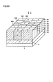
- a structure of a lateral junction field effect transistor 100 according to a first embodiment will now be described with reference to the drawings.
- the lateral junction field effect transistor 100 of the first embodiment has a structural feature that pn-junctions and gate electrode layers are arranged in a vertical direction.
- the vertical direction means a direction of a depth of a substrate
- the lateral direction means a direction parallel to a main surface of the substrate.
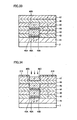
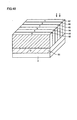
- Lateral junction field effect transistor 100 includes a first semiconductor layer 11, which is located on a semiconductor substrate 2 made of silicon (Si) and others, and is doped with impurities of a p-type, a second semiconductor layer 12, which is located on first semiconductor layer 11, and is doped with impurities of an n-type more heavily (i.e., at a higher concentration) than first semiconductor layer 11, a third semiconductor layer 13 located on second semiconductor layer 12 and doped with p-type impurities, a fourth semiconductor layer 14 located on third semiconductor layer 13 and doped with n-type impurities, and a fifth semiconductor layer 15 located on fourth semiconductor layer 14 and doped with p-type impurities.
- First semiconductor layer 11 is made of Sic, has a layer thickness from about 3 ⁇ m to about 4 ⁇ m and is doped with impurities at a concentration of about 1 x 10 16 cm -3 .
- Each of second, third, fourth and fifth semiconductor layers 12, 13, 14 and 15 is made of SiC, has a layer thickness from about 0.5 ⁇ m to about 1.0 ⁇ m and is doped with impurities at a concentration from about 1 x 10 17 cm -3 to about 3 x 10 17 cm -3 .
- source/drain region layers 6 and 8 are arranged with a predetermined space therebetween.
- Source/drain region layers 6 and 8 have lower surfaces extending on second semiconductor layer 12, and are doped with n-type impurities more heavily than second and fourth semiconductor layers 12 and 14.
- the impurity concentrations of source/drain region layers 6 and 8 are substantially in a range from about 1 x 10 19 cm -3 to about 1 x 10 20 cm -3 .
- First gate electrode layer 18A is arranged in third semiconductor layer 13.
- First gate electrode layer 18A extends in second and third semiconductor layers 12 and 13, has a lower surface extending on second semiconductor layer 12, and is doped with p-type impurities more heavily than second semiconductor layer 12.
- Second gate electrode layer 18B is arranged in fifth semiconductor layer 15.
- Second gate electrode layer 18B has a lower surface extending on fourth semiconductor layer 14, has substantially the same impurity concentration as first gate electrode layer 18A, and has the same potential as first gate electrode layer 18A.
- the impurity concentrations of first and second gate electrode layers 18A and 18B are in a range from about 3 x 10 18 cm -3 to about 1 x 10 20 cm -3 .
- an impurity region layer 4 which extends to first semiconductor layer 11, and is doped with p-type impurities at a concentration from about 3 x 10 18 cm -3 to about 1 x 10 20 cm -3 .
- a normally-off type of the lateral junction field effect transistor can be achieved by such a structure that a distance w11 between a top of first semiconductor layer 11 and a bottom of first gate electrode layer 18A is smaller than a distance of a depletion layer extended by a diffused potential in a junction between second semiconductor layer 12 and first gate electrode layer 18A, and a distance w12 between a top of third semiconductor layer 13 and a bottom of second gate electrode layer 18B is smaller than a distance of a depletion layer extended by a diffused potential in a junction between fourth semiconductor layer 14 and second gate electrode layer 18B.
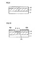
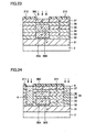
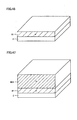
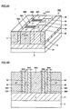
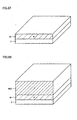
- first semiconductor layer 11 which is made of SiC doped with p-type impurities, and has a layer thickness from about 3 ⁇ m to about 4 ⁇ m and an impurity concentration of about 1 x 10 16 cm -3 , is formed on semiconductor substrate 2 made of silicon and others by epitaxial growth.
- second semiconductor layer 12 which is made of SiC doped with n-type impurities, and has a layer thickness of about 0.5 ⁇ m and an impurity concentration of about 3 x 10 17 cm -3 higher than that of first semiconductor layer 11, is formed on first semiconductor layer 11 by epitaxial growth.
- third semiconductor layer 13 which is made of SiC doped with p-type impurities, and has a layer thickness of about 0.5 ⁇ m and an impurity concentration of about 3 x 10 17 cm -3 , is formed on second semiconductor layer 12 by epitaxial growth.
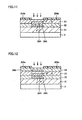
- an oxide film 200 having a predetermined opening pattern is formed on third semiconductor layer 13.
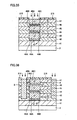
- oxide film 200 as a mask, p-type impurities are implanted into third semiconductor layer 13 to form first gate electrode layer 18A, which extends in second and third semiconductor layers 12 and 13, and is doped with p-type impurities at a concentration from about 3 x 10 18 cm -3 to about 1 x 10 20 cm -3 higher than that of second semiconductor layer 12.
- implantation of the p-type impurities is effected in two stages, i.e., a stage under conditions of an implantation energy of about 700 kev and an implantation dose of about 3 x 10 14 cm -2 , and a stage under conditions of an implantation energy of about 500 kev and an implantation dose of about 3 x 10 14 cm -2 .
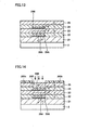
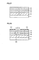
- oxide film 200 is removed, and then fourth semiconductor layer 14, which is made of SiC doped with n-type impurities, and has a thickness of about 0.5 ⁇ m and an impurity concentration of about 3 x 10 17 cm -3 , is formed on third semiconductor layer 13 by epitaxial growth.
- fifth semiconductor layer 15, which is made of SiC doped with p-type impurities, and has a thickness of about 0.5 ⁇ m and an impurity concentration of about 3 x 10 17 cm -3 is formed on fourth semiconductor layer 14 by epitaxial growth.
- an oxide film 201 having a predetermined opening pattern is formed on fifth semiconductor layer 15, and p-type impurities are implanted into fifth semiconductor layer 15 masked with oxide film 201 to form second gate electrode layer 18B, which has a lower surface extending on fourth semiconductor layer 14, contains p-type impurities at a concentration from about 3 x 10 18 cm -3 to about 1 x 10 20 cm -3 , i.e., at a concentration substantially equal to that of first gate electrode layer 18A, and has the same potential as first gate electrode layer 18A.
- This implantation of the p-type impurities is performed in six stages under different conditions, i.e., a first stage under conditions of an implantation energy of about 700 kev and an implantation dose of about 3 x 10 14 cm -2 , a second stage under conditions of an implantation energy of about 500 kev and an implantation dose of about 3 x 10 14 cm -2 , a third stage under conditions of an implantation energy of about 280 kev and an implantation dose of about 5 x 10 14 cm -2 , a fourth stage under conditions of an implantation energy of about 140 kev and an implantation dose of about 5 x 10 14 cm -2 , a fifth stage under conditions of an implantation energy of about 70 kev and an implantation dose of about 4 x 10 14 cm -2 , and a sixth stage under conditions of an implantation energy of about 30 kev and an implantation dose of about 3 x 10 14 cm -2 .
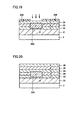
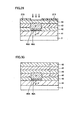
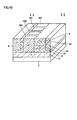
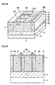
- oxide film 201 is removed, and an oxide film 202 having a predetermined opening pattern is formed on fifth semiconductor layer 15. Then, impurities are implanted into fifth semiconductor layer 15 masked with oxide film 202, and more specifically into portions on the opposite sides of first and second gate electrode layers 18A and 18B to form source/drain region layers 6 and 8, which has the lower surfaces extending on the second semiconductor layer 12, and contain n-type impurities at a concentration from about 1 x 10 19 cm -3 to about 1 x 10 20 cm -3 , i.e., at a concentration higher than that of second and fourth semiconductor layers 12 and 14.
- oxide film 202 is removed, and then an oxide film 203 having a predetermined opening pattern is formed on fifth semiconductor layer 15. Impurities are implanted into fifth semiconductor layer 15 masked with oxide film 202, and more specifically into a portion outside source/drain region layer 6 to form impurity region layer 4, which has a lower surface extending on first semiconductor layer 11, and contains p-type impurities at a concentration from about 3 x 10 18 cm -3 to about 1 x 10 20 cm -3 .
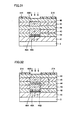
- the structure is then processed in various steps of surface thermal oxidization, opening, formation of Ni-electrode, formation of insulating layers (OCD and others), opening of contact holes, provision of aluminum interconnections, formation of pads, thermal processing, formation of ohmic contacts and others.
- lateral junction field effect transistor 100 of the first embodiment shown in Fig. 1 is completed.
- the lateral junction field effect transistor having the above structure as well as the method of manufacturing the same, since the plurality of the lateral junction field effect transistors are stacked in a vertical direction, the on-resistance of the element can be reduced, as compared with conventional structures.
- the second, third, fourth and fifth semiconductor layers 12, 13, 14 and 15 may have substantially the same impurity concentration and the same layer thickness so that the lateral junction field effect transistors can have the minimum on-resistance and the maximum breakdown voltage.
- One or more unit transistor structure(s) each being substantially the same as the structure having second semiconductor layer 12, third semiconductor layer 13 and first gate electrode layer 18A may be arranged between third and fourth semiconductor layers 13 and 14. Thereby, the junction field effect transistor can have further improved characteristics.
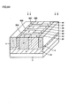
- a lateral junction field effect transistor 200 according to a second embodiment will now be described with reference to Fig. 8.
- Lateral junction field effect transistor 200 has a structural feature that pri-junetions and gate electrode layers are arranged in a vertical direction, similarly to the lateral junction field effect transistor 100 already described.
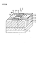
- Lateral junction field effect transistor 200 includes a first semiconductor layer 21, which is located on semiconductor substrate 2 made of silicon and others, and is doped with p-type impurities, a second semiconductor layer 22, which is located on first semiconductor layer 21, and is doped with n-type impurities more heavily than first semiconductor layer 21, a third semiconductor layer 23 located on second semiconductor layer 22 and doped with p-type impurities, a fourth semiconductor layer 24 located on third semiconductor layer 23 and doped with n-type impurities, and a fifth semiconductor layer 25 located on fourth semiconductor layer 24 and doped with p-type impurities.
- First semiconductor layer 21 is made of SiC, has a layer thickness from about 3 ⁇ m to about 4 ⁇ m and is doped with impurities at a concentration of about 1 x 10 16 cm -3 .
- Each of second, third, fourth and fifth semiconductor layers 22, 23, 24 and 25 is made of SiC, has a layer thickness from about 0.5 ⁇ m to about 1.0 ⁇ m and is doped with impurities at a concentration from about 1 x 10 17 cm -3 to about 3 x 10 17 cm -3 .
- source/drain region layers 6 and 8 are arranged with a predetermined space therebetween.
- Source/drain region layers 6 and 8 have lower surfaces extending on second semiconductor layer 22, and are doped with n-type impurities more heavily than second and fourth semiconductor layers 22 and 24.
- the impurity concentrations of source/drain region layers 6 and 8 are substantially in a range from about 1 x 10 19 cm -3 to about 1 x 10 20 cm -3 .
- First gate electrode layer 28A is arranged in third semiconductor layer 23.
- First gate electrode layer 28A has a lower surface extending on second semiconductor layer 22, and is doped with p-type impurities more heavily than second semiconductor layer 22.
- a second gate electrode layer 28B is arranged in fifth semiconductor layer 25.
- Second gate electrode layer 28B has a lower surface extending on fourth semiconductor layer 24, has substantially the same impurity concentration as first gate electrode layer 28A, and has the same potential as first gate electrode layer 28A.
- the impurity concentrations of first and second gate electrode layers 28A and 28B are in a range from about 3 x 10 18 cm -3 to about 1 x 10 20 cm -3 .
- a first impurity doped region 29A of the p-type is arranged in second semiconductor layer 22 between first semiconductor layer 21 and first gate electrode layer 28A.
- First impurity doped region 29A has substantially the same impurity concentration as first gate electrode layer 28A, and has the same potential as first gate electrode layer 28A.
- a second impurity doped region 29B of the p-type is arranged in fourth semiconductor layer 24 between third semiconductor layer 23 and second gate electrode layer 28B.
- Second impurity doped region 29B has substantially the same impurity concentration as first gate electrode layer 28A, and has the same potential as first gate electrode layer 28A.
- first impurity doped region 29A and one layer of second impurity doped region 29B it may be provided with a plurality of layers of first impurity doped regions 29A and a plurality of layers of second impurity doped regions 29B for the purpose of achieving the normally-off type of the lateral junction field effect transistor, in which a total channel width is increased and an on-resistance is lowered.
- impurity region layer 4 which extends to first semiconductor layer 21, and is doped with p-type impurities at a concentration from about 3 x 10 18 cm -3 to about 1 x 10 20 cm -3 .
- the normally-off type of the lateral junction field effect transistor can be achieved by such a structure that a distance w21 between a top of first semiconductor layer 21 and a bottom of first impurity doped region 29A is smaller than a distance of a depletion layer extended by a diffused potential in a junction between second semiconductor layer 22 and first impurity doped region 29A, a distance w22 between a top of first impurity doped region 29A and a bottom of first gate electrode layer 28A is smaller than double a distance of a depletion layer extended by a diffused potential in a junction between second semiconductor layer 22 and first gate electrode layer 28A, a distance w23 between a top of third semiconductor layer 23 and a bottom of second impurity doped region 29B is smaller than a distance of a depletion layer extended by a diffused potential in a junction between fourth semiconductor layer 24 and second impurity doped region 29B, and a distance w24 between a top of second impurity doped region 29B and a bottom
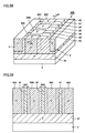
- first semiconductor layer 21 which is made of SiC doped with p-type impurities, and has a layer thickness from about 3 ⁇ m to about 4 ⁇ m and an impurity concentration of about 1 x 10 16 cm -3 , is formed on semiconductor substrate 2 made of silicon and others by epitaxial growth.
- second semiconductor layer 22 which is made of SiC doped with n-type impurities, and has a layer thickness of about 0.5 ⁇ m and an impurity concentration of about 3 x 10 17 cm -3 higher than that of first semiconductor layer 11, is formed on first semiconductor layer 21 by epitaxial growth.
- an oxide film 204a having a predetermined opening pattern is formed on second semiconductor layer 22.
- oxide film 204a as a mask, p-type impurities are implanted into second semiconductor layer 22 to form first impurity doped region 29A, which is located in second semiconductor layer 22, and is doped with p-type impurities at a concentration from about 3 x 10 18 cm -3 to about 1 x 10 20 cm -3 .
- This implantation of the p-type impurities is effected under conditions of an implantation energy of about 270 kev and an implantation dose of about 7 x 10 13 cm -2 .
- oxide film 204a is removed, and then third semiconductor layer 23, which is made of SiC doped with p-type impurities, and has a layer thickness from about 0.5 ⁇ m and an impurity concentration of about 3 x 10 17 cm -3 , is formed on second semiconductor layer 22 by epitaxial growth.
- An oxide film 204b having a predetermined opening pattern is formed on third semiconductor layer 23.
- oxide film 204b as a mask, p-type impurities are implanted into third semiconductor layer 23 to form first gate electrode layer 28A, which extends in second and third semiconductor layers 22 and 23, and is doped with p-type impurities at a concentration from about 3 x 10 18 cm -3 to about 1 x 10 20 cm -3 higher than that of second semiconductor layer 22.
- This implantation of the p-type impurities is effected under conditions of an implantation energy of about 350 kev and an implantation dose of about 1 x 10 14 cm -2 .
- oxide film 204b is removed, and then fourth semiconductor layer 24, which is made of SiC doped with n-type impurities, and has a thickness of about 0.5 ⁇ m and an impurity concentration of about 3 x 10 17 cm -3 higher than that of first semiconductor layer 11, is formed on third semiconductor layer 23.
- an oxide film 205a having a predetermined opening pattern is formed on fourth semiconductor layer 24, and p-type impurities are implanted into fourth semiconductor layer 24 masked with oxide film 205a to form second impurity doped region 29B, which is located in fourth semiconductor layer 24 and contains p-type impurities at a concentration from about 3 x 10 18 cm -3 to about 1 x 10 20 cm -3 .
- This implantation of the p-type impurities is performed under conditions of an implantation energy of about 270 kev and an implantation dose of about 7 x 10 13 cm -2 .
- fifth semiconductor layer 25 which is made of SiC doped with p-type impurities, and has a thickness of about 0.5 ⁇ m and an impurity concentration of about 3 x 10 17 cm -3 , is formed on fourth semiconductor layer 24 by epitaxial growth.
- an oxide film 205b having a predetermined opening pattern is formed on fifth semiconductor layer 25, and p-type impurities are implanted into fifth semiconductor layer 25 masked with oxide film 205b to form second gate electrode layer 28B, which extends in fourth and fifth semiconductor layers, contains p-type impurities at a concentration from about 3 x 10 18 cm -3 to about 1 x 10 20 cm -3 , i.e., at a concentration higher than that of second semiconductor layer 22.
- This implantation of the p-type impurities is performed in five stages under different conditions, i.e., a first stage under conditions of an implantation energy of about 350 kev and an implantation dose of about 1 x 10 14 cm -2 , a second stage under conditions of an implantation energy of about 250 kev and an implantation dose of about 2 x 10 14 cm -2 , a third stage under conditions of an implantation energy of about 140 kev and an implantation dose of about 5 x 10 14 cm -2 , a fourth stage under conditions of an implantation energy of about 70 kev and an implantation dose of about 4 x 10 14 cm -2 , and a fifth stage under conditions of an implantation energy of about 30 kev and an implantation dose of about 3 x 10 14 cm -2 .
- oxide films 205 is removed, and an oxide film 206 having a predetermined opening pattern is formed on fifth semiconductor layer 15. Then, impurities are implanted into fifth semiconductor layer 15 masked with oxide film 206, and more specifically into portions on the opposite sides of first and second impurity doped regions 29A and 29B as well as first and second gate electrode layers 28A and 28B to form source/drain region layers 6 and 8, which have lower surfaces extending on second semiconductor layer 22, and are doped with n-type impurities at a concentration from about 1 x 10 19 cm -3 to about 1 x 10 20 cm -3 higher than those of second and fourth semiconductor layers 22 and 24.
- oxide film 206 is removed, and then an oxide film 207 having a predetermined opening pattern is formed on fifth semiconductor layer 15. Then, impurities are implanted into fifth semiconductor layer 15 masked with oxide film 207, and more specifically into a portion outside source/drain region layer 6 to form impurity region layer 4, which has a lower surface extending on first semiconductor layer 21, and contains p-type impurities at a concentration from about 3 x 10 18 cm -3 to about 1 x 10 20 cm -3 .
- the structure is then processed in various steps of surface thermal oxidization, opening, formation of Ni-electrode, formation of insulating layers (OCD and others), opening of contact holes, provision of aluminum interconnections, formation of pads, thermal processing, formation of ohmic contacts and others.
- lateral junction field effect transistor 200 of the second embodiment shown in Fig. 8 is completed.
- the lateral junction field effect transistor having the above structure as well as the method of manufacturing the same, since the plurality of the lateral junction field effect transistors are stacked in the vertical direction, the on-resistance of the element can be reduced, as compared with conventional structures.
- the second, third, fourth and fifth semiconductor layers 22, 23, 24 and 25 may have substantially the same impurity concentration and the same layer thickness so that the lateral junction field effect transistors can have the minimum on-resistance and the maximum breakdown voltage.
- One or more unit transistor structure(s) each being substantially the same as the structure having second semiconductor layer 22, third semiconductor layer 23 and first gate electrode layer 28A may be arranged between third and fourth semiconductor layers 23 and 24. Thereby, the junction field effect transistor can have further improved characteristics.
- a lateral junction field effect transistor 300 according to a third embodiment will now be described with reference to Fig. 17.
- Lateral junction field effect transistor 300 has a structural feature that pn-junctions and gate electrode layers are arranged in a vertical direction, similarly to the lateral junction field effect transistor 100 already described.
- Lateral junction field effect transistor 300 includes a first semiconductor layer 31, which is located on semiconductor substrate 2 made of silicon and others, and is doped with p-type impurities, a second semiconductor layer 32, which is located on first semiconductor layer 31, and is doped with n-type impurities more heavily than first semiconductor layer 31, a third semiconductor layer 33 located on second semiconductor layer 32 and doped with p-type impurities, a fourth semiconductor layer 34 located on third semiconductor layer 33 and doped with n-type impurities, a fifth semiconductor layer 35 located on fourth semiconductor layer 34 and doped with p-type impurities, a sixth semiconductor layer 36 located on fifth semiconductor layer 35 and doped with n-type impurities, and a seventh semiconductor layer 37 located on sixth semiconductor layer 36 and doped with p-type impurities.
- First semiconductor layer 31 is made of SiC, has a layer thickness from about 3 ⁇ m to about 4 ⁇ m and is doped with impurities at a concentration of about 1 x 10 16 cm -3 .
- Each of second, third, fourth, fifth, sixth and seventh semiconductor layers 32, 33, 34, 35, 36 and 37 is made of SiC, has a layer thickness from about 0.5 ⁇ m to about 1.0 ⁇ m and is doped with impurities at a concentration from about 1 x 10 17 cm -3 to about 3 x 10 17 cm -3 .
- source/drain region layers 6 and 8 are arranged with a predetermined space therebetween.
- Source/drain region layers 6 and 8 have lower surfaces extending on second semiconductor layer 32, and are doped with n-type impurities more heavily than second, fourth and sixth semiconductor layers 32, 34 and 36.
- the impurity concentrations of source/drain region layers 6 and 8 are substantially in a range from about 1 x 10 19 cm -3 to about 1 x 10 20 cm -3 .
- First gate electrode layer 38A is arranged in third semiconductor layer 33.
- First gate electrode layer 38A has lower and upper surfaces extending on second and fourth semiconductor layers 32 and 34, respectively, and is doped with p-type impurities more heavily than second and fourth semiconductor layers 32 and 34.
- Second gate electrode layer 38B is arranged in fifth semiconductor layer 35.
- Second gate electrode layer 38B has lower and upper surfaces extending on fourth and sixth semiconductor layers 34 and 36, respectively, and is doped with p-type impurities more heavily than fourth and sixth semiconductor layers 34 and 36.
- Third gate electrode layer 38C is arranged in seventh semiconductor layer 37.
- Third gate electrode layer 38C has a lower surface extending on sixth semiconductor layer 36, has substantially the same impurity concentration as first and second gate electrode layers 38A and 38B, and has the same potential as first and second gate electrode layers 38A and 38B.
- the impurity concentrations of first, second and third gate electrode layers 38A, 38B and 38C are in a range from about 3 x 10 18 cm -3 to about 1 x 10 20 cm -3 .
- impurity region layer 4 which extends to first semiconductor layer 31, and is doped with p-type impurities at a concentration from about 3 x 10 18 cm -3 to about 1 x 10 20 cm -3 .
- the normally-off type of the lateral junction field effect transistor can be achieved by such a structure that a distance w31 between a top of first semiconductor layer 31 and a bottom of first gate electrode layer 38A is smaller than a distance of a depletion layer extended by a diffused potential in a junction between second semiconductor layer 32 and first gate electrode layer 38A, and a distance w32 between a top of first gate electrode layer 38A and a bottom of second gate electrode layer 38B is smaller than double a distance of a depletion layer extended by a diffused potential in a junction between fourth semiconductor layer 34 and first gate electrode layer 38A.
- a method of manufacturing lateral junction field effect transistor 300 having the above structures will now be described with reference to Figs. 18 to 25.
- first semiconductor layer 31 which is made of SiC doped with p-type impurities, and has a layer thickness from about 3 ⁇ m to about 4 ⁇ m and an impurity concentration of about 1 x 10 16 cm -3 , is formed on semiconductor substrate 2 made of silicon and others by epitaxial growth.
- second semiconductor layer 32 which is made of SiC doped with n-type impurities, and has a layer thickness from about 0.5 ⁇ m to about 1.0 ⁇ m and an impurity concentration from about 1 x 10 17 cm -3 to about 3 x 10 17 cm -3 higher than that of first semiconductor layer 31, is formed on first semiconductor layer 31 by epitaxial growth.
- third semiconductor layer 33 which is made of SiC doped with p-type impurities, and has a layer thickness from about 0.5 ⁇ m to about 1.0 ⁇ m and an impurity concentration from about 1 x 10 17 cm -3 to about 3 x 10 17 cm -3 , is formed on second semiconductor layer 32 by epitaxial growth.
- fourth semiconductor layer 34 which is made of SiC doped with n-type impurities, and has a layer thickness from about 0.5 ⁇ m to about 1.0 ⁇ m and an impurity concentration from about 1 x 10 17 cm -3 to about 3 x 10 17 cm -3 , is formed on third semiconductor layer 33 by epitaxial growth.
- an oxide film 208 having a predetermined opening pattern is formed on fourth semiconductor layer 34.
- oxide film 208 as a mask, p-type impurities are implanted into a predetermined region of fourth semiconductor layer 34 to form first gate electrode layer 38A, which has lower and upper surfaces extending on second and fourth semiconductor layers 32 and 34, respectively, and is doped with p-type impurities at a concentration from about 3 x 10 18 cm -3 to about 1 x 10 20 cm -3 higher than that of second and fourth semiconductor layers 32 and 34.
- fifth semiconductor layer 35 which is made of SiC doped with p-type impurities, and has a thickness from about 0.5 ⁇ m to about 1.0 ⁇ m and an impurity concentration from about 1 x 10 17 cm -3 to about 3 x 10 17 cm -3 , is formed on fourth semiconductor layer 34.
- sixth semiconductor layer 36 which is made of SiC doped with n-type impurities, and has a thickness from about 0.5 ⁇ m to about 1.0 ⁇ m and an impurity concentration from about 1 x 10 17 cm -3 to about 3 x 10 17 cm -3 , is formed on fifth semiconductor layer 35 by epitaxial growth.
- an oxide film 209 having a predetermined opening pattern is formed on sixth semiconductor layer 36, and p-type impurities are implanted into a predetermined region of sixth semiconductor layer 36 masked with oxide film 209 to form second gate electrode layer 38B, which has lower and upper surfaces extending on fourth and sixth semiconductor layers 34 and 36, respectively, and contains p-type impurities at a concentration from about 3 x 10 18 cm -3 to about 1 x 10 20 cm -3 higher than those of fourth and sixth semiconductor layers 34 and 36.
- seventh semiconductor layer 37 which is made of SiC doped with p-type impurities, and has a thickness from about 0.5 ⁇ m to about 1.0 ⁇ m and an impurity concentration from about 1 x 10 17 cm -3 to about 3 x 10 17 cm -3 , is formed on sixth semiconductor layer 36 by epitaxial growth.
- an oxide film 210 having a predetermined opening pattern is formed on seventh semiconductor layer 37, and p-type impurities are implanted into a predetermined region of seventh semiconductor layer 37 masked with oxide film 210 to form a third gate electrode layer 38C, which has a lower surface extending on sixth semiconductor layer 36, and contains p-type impurities at a concentration from about 3 x 10 18 cm -3 to about 1 x 10 20 cm -3 higher than that of sixth semiconductor layer 36.
- oxide film 210 is removed, and an oxide film 211 having a predetermined opening pattern is formed on seventh semiconductor layer 37. Then, impurities are implanted into seventh semiconductor layer 37 masked with oxide film 211, and more specifically into portions on the opposite sides of first, second and third gate electrode layers 38A, 38B and 38C to form source/drain region layers 6 and 8, which have lower surfaces extending on second semiconductor layer 32, and are doped with n-type impurities at a concentration from about 1 x 10 19 cm -3 to about 1 x 10 20 cm -3 higher than those of second and fourth semiconductor layers 32 and 34.
- oxide film 211 is removed, and then an oxide film 212 having a predetermined opening pattern is formed on seventh semiconductor layer 37. Then, impurities are implanted into seventh semiconductor layer 37 masked with oxide film 212, and more specifically into a portion outside source/drain region layer 6 to form impurity region layer 4, which has the lower surface extending on first semiconductor layer 31, and contains p-type impurities at a concentration from about 3 x 10 18 cm -3 to about 1 x 10 20 cm -3 .
- the structure is then processed in various steps of surface thermal oxidization, opening, formation of Ni-electrode, formation of insulating layers (OCD and others), opening of contact holes, provision of aluminum interconnections, formation of pads, thermal processing, formation of ohmic contacts and others.
- lateral junction field effect transistor 300 of the third embodiment shown in Fig. 17 is completed.
- the lateral junction field effect transistor having the above structure as well as the method of manufacturing the same, since the plurality of the lateral junction field effect transistors are stacked in the vertical direction, the on-resistance of the element can be reduced, as compared with conventional structures.
- the second, third, fourth, fifth, sixth and seventh semiconductor layers 32, 33, 34, 35, 36 and 37 may have substantially the same impurity concentration and the same layer thickness so that the lateral junction field effect transistors can have the minimum on-resistance and the maximum breakdown voltage.
- One or more unit transistor structure(s) each being substantially the same as the structure having third semiconductor layer 33, fourth semiconductor layer 34 and first gate electrode layer 38A may be arranged between fourth and fifth semiconductor layers 34 and 35. Thereby, the junction field effect transistor can have further improved characteristics.
- a lateral junction field effect transistor 400 according to a fourth embodiment will now be described with reference to Fig. 26.
- Lateral junction field effect transistor 400 has a structural feature that pn-junctions and gate electrode layers are arranged in a vertical direction, similarly to the lateral junction field effect transistor 100 already described.
- Lateral junction field effect transistor 400 includes a first semiconductor layer 41, which is located on semiconductor substrate 2 made of silicon and others, and is doped with p-type impurities, a second semiconductor layer 42, which is located on first semiconductor layer 41, and is doped with n-type impurities more heavily than first semiconductor layer 41, a third semiconductor layer 43 located on second semiconductor layer 42 and doped with p-type impurities, a fourth semiconductor layer 44 located on third semiconductor layer 43 and doped with n-type impurities, a fifth semiconductor layer 45 located on fourth semiconductor layer 44 and doped with p-type impurities, a sixth semiconductor layer 46 located on fifth semiconductor layer 45 and doped with n-type impurities, and a seventh semiconductor layer 47 located on sixth semiconductor layer 46 and doped with p-type impurities.
- First semiconductor layer 41 is made of SiC, has a layer thickness from about 3 ⁇ m to about 4 ⁇ m and is doped with impurities at a concentration of about 1 x 10 16 cm -3 .
- Each of second, third, fourth, fifth, sixth and seventh semiconductor layers 42, 43, 44, 45, 46 and 47 is made of SiC, has a layer thickness from about 0.5 ⁇ m to about 1.0 ⁇ m and is doped with impurities at a concentration from about 1 x 10 17 cm -3 to about 3 x 10 17 cm -3 .
- source/drain region layers 6 and 8 are arranged with a predetermined space therebetween.
- Source/drain region layers 6 and 8 have lower surfaces extending on second semiconductor layer 42, and are doped with n-type impurities more heavily than second, fourth and sixth semiconductor layers 42, 44 and 46.
- the impurity concentrations of source/drain region layers 6 and 8 are substantially in a range from about 1 x 10 19 cm -3 to about 1 x 10 20 cm -3 .
- First gate electrode layer 48A is arranged in third semiconductor layer 43.
- First gate electrode layer 48A has lower and upper surfaces extending on second and fourth semiconductor layers 42 and 44, respectively, and is doped with impurities more heavily than second, fourth and sixth semiconductor layers 42, 44 and 46.
- Second gate electrode layer 48B has lower and upper surfaces extending on fourth and sixth semiconductor layers 44 and 46, respectively has substantially the same impurity concentration as first gate electrode layer 28A, and has the same potential as first gate electrode layer 28A.
- a third gate electrode layer 48C doped with p-type impurities is arranged in seventh semiconductor layer 47.
- Third gate electrode layer 48C has a lower surface extending on sixth semiconductor layer 46, has substantially the same impurity concentration as first and second gate electrode layers 48A and 48B, and has the same potential as first and second gate electrode layers 48A and 48B.
- the impurity concentrations of first, second and third gate electrode layers 48A, 48B and 48C are in a range from about 3 x 10 18 cm -3 to about 1 x 10 20 cm -3 .
- a first impurity doped region 39A of the p-type is arranged in second semiconductor layer 42 between first semiconductor layer 41 and first gate electrode layer 48A.
- First impurity doped region 39A has substantially the same impurity concentration as first gate electrode layer 48A, and has the same potential as first gate electrode layer 48A.
- a second impurity doped region 49B of the p-type is arranged in fourth semiconductor layer 44 between first and second gate electrode layers 48A and 48B.
- Second impurity doped region 49B has substantially the same impurity concentration as first gate electrode layer 48A, and has the same potential as first gate electrode layer 48A.
- a third impurity doped region 49C of the p-type is arranged in sixth semiconductor layer 46 between second and third gate electrode layers 48B and 48C.
- Third impurity doped region 49C has substantially the same impurity concentration as first and second gate electrode layers 48A and 48B, and has the same potential as first and second gate electrode layers 48A and 48B.
- first, second and third impurity doped regions 49A, 49B and 49C each formed of one layer
- each of first, second and third impurity doped regions 49A, 49B and 49C may be formed of a plurality of layers for the purpose of achieving the normally-off type of the lateral junction field effect transistor, in which the total channel width is increased and the on-resistance is lowered.
- impurity region layer 4 which extends to first semiconductor layer 41, and is doped with p-type impurities at a concentration from about 3 x 10 18 cm -3 to about 1 x 10 20 cm -3 .
- the normally-off type of the lateral junction field effect transistor can be achieved by such a structure that a distance w41 between a top of first semiconductor layer 41 and a bottom of first gate electrode layer 48A is smaller than a distance of a depletion layer extended by a diffused potential in a junction between second semiconductor layer 42 and first gate electrode layer 48A, and a distance w42 between a top of first gate electrode layer 48A and a bottom of second gate electrode layer 48B is smaller than a sum of a distance of a depletion layer extended by a diffused potential in a junction between fourth semiconductor layer 44 and first gate electrode layer 48A and a distance of a depletion layer extended by a diffused potential in a junction between fourth semiconductor layer 44 and second gate electrode layer 48B.
- a distance w43 between a top of first semiconductor layer 41 and a bottom of first impurity doped region 49A is smaller than a distance of a depletion layer extended by a diffused potential in a junction between second semiconductor layer 42 and first impurity doped region 49A
- a distance w44 between a top of first impurity doped region 49A and a bottom of first gate electrode layer 48A is smaller than double a distance of a depletion layer extended by a diffused potential in a junction between second semiconductor layer 42 and first gate electrode layer 48A
- a distance w45 between a top of first gate electrode layer 48A and a bottom of second impurity doped region 49B is smaller than double a distance of a depletion layer extended by a diffused potential in a junction between fourth semiconductor layer 44 and second impurity doped region 49B
- a distance w46 between a top of second impurity doped region 49B and a bottom of second gate electrode layer 48B is smaller than a distance of
- first semiconductor layer 41 which is made of SiC doped with p-type impurities, and has a layer thickness from about 3 ⁇ m to about 4 ⁇ m and an impurity concentration of about 1 x 10 16 cm -3 , is formed on semiconductor substrate 2 made of silicon and others by epitaxial growth.
- second semiconductor layer 42 which is made of SiC doped with n-type impurities, and has a layer thickness from about 0.5 ⁇ m to about 1.0 ⁇ m and an impurity concentration from about 1 x 10 17 cm -3 to about 3 x 10 17 cm -3 higher than that of first semiconductor layer 41, is formed on first semiconductor layer 41 by epitaxial growth.
- third semiconductor layer 43 which is made of SiC doped with p-type impurities, and has a layer thickness from about 0.5 ⁇ m to about 1.0 ⁇ m and an impurity concentration from about 1 x 10 17 cm -3 to about 3 x 10 17 cm -3 , is formed on second semiconductor layer 42 by epitaxial growth.
- fourth semiconductor layer 44 which is made of SiC doped with n-type impurities, and has a layer thickness from about 0.5 ⁇ m to about 1.0 ⁇ m and an impurity concentration from about 1 x 10 17 cm -3 to about 3 x 10 17 cm -3 , is formed on third semiconductor layer 43 by epitaxial growth.
- an oxide film 213 having a predetermined opening pattern is formed on fourth semiconductor layer 44.
- oxide film 213 as a mask, p-type impurities are implanted into a predetermined region of fourth semiconductor layer 44 to form first gate electrode layer 48A, which has lower and upper surfaces extending on second and fourth semiconductor layers 42 and 44, respectively, and is doped with p-type impurities at a concentration from about 3 x 10 18 cm -3 to about 1 x 10 20 cm -3 higher than that of second and fourth semiconductor layers 42 and 44.
- oxide film 213 is still used as a mask, and p-type impurities are implanted into second semiconductor layer 42 to form first impurity doped region 49A, which has substantially the same impurity concentration as first gate electrode layer 48A, i.e., an impurity concentration from about 3 x 10 18 cm -3 to about 1 x 10 20 cm -3 , and has the same potential as first gate electrode layer 48A.
- fifth semiconductor layer 45 which is made of SiC doped with p-type impurities, and has a thickness from about 0.5 ⁇ m to about 1.0 ⁇ m and an impurity concentration from about 1 x 10 17 cm -3 to about 3 x 10 17 cm -3 , is formed on fourth semiconductor layer 34.
- sixth semiconductor layer 46 which is made of SiC doped with n-type impurities, and has a thickness from about 0.5 ⁇ m to about 1.0 ⁇ m and an impurity concentration from about 1 x 10 17 cm -3 to about 3 x 10 17 cm -3 , is formed on fifth semiconductor layer 45.
- an oxide film 214 having a predetermined opening pattern is formed on sixth semiconductor layer 46, and p-type impurities are implanted into a predetermined region of sixth semiconductor layer 46 masked with oxide film 214 to form second gate electrode layer 48B, which has lower and upper surfaces extending on fourth and sixth semiconductor layers 44 and 46, respectively, and contains p-type impurities at a concentration from about 3 x 10 18 cm -3 to about 1 x 10 20 cm -3 higher than those of fourth and sixth semiconductor layers 44 and 46.
- oxide film 214 is still used as a mask, and p-type impurities are implanted into fourth semiconductor layer 44 to form second impurity doped region 49B, which has substantially the same impurity concentration as first gate electrode layer 48A, i.e., the impurity concentration from about 3 x 10 18 cm -3 to about 1 x 10 20 cm -3 , and has the same potential as first gate electrode layer 48A.
- seventh semiconductor layer 47 which is made of SiC doped with p-type impurities, and has a thickness from about 0.5 ⁇ m to about 1.0 ⁇ m and an impurity concentration from about 1 x 10 17 cm -3 to about 3 x 10 17 cm -3 , is formed on sixth semiconductor layer 46 by epitaxial growth.
- an oxide film 215 having a predetermined opening pattern is formed on seventh semiconductor layer 37, and p-type impurities are implanted into a predetermined region of seventh semiconductor layer 37 masked with oxide film 215 to form third gate electrode layer 48C, which has a lower surface extending on sixth semiconductor layer 46, and contains p-type impurities at a concentration from about 3 x 10 18 cm -3 to about 1 x 10 20 cm -3 higher than that of sixth semiconductor layer 46.
- oxide film 215 is still used as a mask, and p-type impurities are implanted into sixth semiconductor layer 46 to form third impurity doped region 49C, which has substantially the same impurity concentration as first gate electrode layer 48A, i.e., the impurity concentration from about 3 x 10 18 cm -3 to about 1 x 10 20 cm -3 , and has the same potential as first gate electrode layer 48A.
- oxide film 215 is removed, and an oxide film 216 having a predetermined opening pattern is formed on seventh semiconductor layer 37. Then, impurities are implanted into seventh semiconductor layer 47 masked with oxide film 216, and more specifically into portions on the opposite sides of first, second and third gate electrode layers 48A, 48B and 48C as well as first, second and third impurity doped regions 49A, 49B and 49C to form source/drain region layers 6 and 8, which have lower surfaces extending on second semiconductor layer 42, and are doped with n-type impurities at a concentration from about 1 x 10 19 cm -3 to about 1 x 10 20 cm -3 higher than those of second and fourth semiconductor layers 42 and 44.
- oxide film 216 is removed, and then an oxide film 217 having a predetermined opening pattern is formed on seventh semiconductor layer 37. Then, impurities are implanted into seventh semiconductor layer 47 masked with oxide film 217, and more specifically into a portion outside source/drain region layer 6 to form impurity region layer 4, which has the lower surface extending on first semiconductor layer 41, and contains p-type impurities at a concentration from about 3 x 10 18 cm -3 to about 1 x 10 20 cm -3 .
- the structure is then processed in various steps of surface thermal oxidization, opening, formation of Ni-electrode, formation of insulating layers (OCD and others), opening of contact holes, provision of aluminum interconnections, formation of pads, thermal processing, formation of ohmic contacts and others.
- lateral junction field effect transistor 400 of the fourth embodiment shown in Fig. 26 is completed.
- ion implantation must be performed several times for forming an inter-gate connection region layer (not shown), if it has a large depth.
- the impurity implantation for forming the inter-gate connection region layer is performed even in the ion implantation stages for forming the gate electrode layers and the impurity doped regions.
- the inter-gate connection region layer is provided for electrically connecting the plurality of gate electrode layers and impurity doped regions to equalize the potential thereof, and is formed of a connection layer, which is located, e.g., at an end of a device, and extends vertically through the gate electrode layers and the impurity doped regions. In general, the connection layer does not reach the first semiconductor layer.
- the lateral junction field effect transistor having the above structure as well as the method of manufacturing the same, since the plurality of the lateral junction field effect transistors are stacked in the vertical direction, the on-resistance of the element can be reduced, as compared with conventional structures.
- the second, third, fourth, fifth, sixth and seventh semiconductor layers 42, 43, 44, 45, 46 and 47 may have substantially the same impurity concentration and the same layer thickness so that the lateral junction field effect transistors can have the minimum on-resistance and the maximum breakdown voltage.
- One or more unit transistor structure(s) each being substantially the same as the structure having third semiconductor layer 43, fourth semiconductor layer 44, first gate electrode layer 48A and second impurity doped region 49B may be arranged between fourth and fifth semiconductor layers 44 and 45. Thereby, the junction field effect transistor can have further improved characteristics.
- a lateral junction field effect transistor 500 according to a fifth embodiment will now be described with reference to Figs. 38 to 40.
- Lateral junction field effect transistor 500 has a structural feature that pn-junctions are arranged in a vertical direction, and gate electrode layers are arranged in a lateral direction.
- Lateral junction field effect transistor 500 includes a first semiconductor layer 51, which is located on semiconductor substrate 2 made of silicon and others, and is doped with p-type impurities, a second semiconductor layer 52, which is located on first semiconductor layer 51, and is doped with n-type impurities more heavily than first semiconductor layer 51, a third semiconductor layer 53 located on second semiconductor layer 52 and doped with p-type impurities, a fourth semiconductor layer 54 located on third semiconductor layer 53 and doped with n-type impurities, and a fifth semiconductor layer 55 located on fourth semiconductor layer 54 and doped with p-type impurities.
- First semiconductor layer 51 is made of SiC, has a layer thickness from about 3 ⁇ m to about 4 ⁇ m and is doped with impurities at a concentration of about 1 x 10 16 cm -3 .
- Each of second, third, fourth and fifth semiconductor layers 52, 53, 54 and 55 is made of SiC, has a layer thickness from about 0.5 ⁇ m to about 1.0 ⁇ m and is doped with impurities at a concentration from about 1 x 10 17 cm -3 to about 3 x 10 17 cm -3 .
- source/drain region layers 6 and 8 are arranged with a predetermined space therebetween.
- Source/drain region layers 6 and 8 have lower surfaces extending on second semiconductor layer 52, and are doped with n-type impurities more heavily than second and fourth semiconductor layers 52 and 54.
- the impurity concentrations of source/drain region layers 6 and 8 are substantially in a range from about 1 x 10 19 cm -3 to about 1 x 10 20 cm -3 .
- First gate electrode layer 58A is arranged in fifth semiconductor layer 55.
- First gate electrode layer 58A has a lower surface extending on second semiconductor layer 52, and is doped with p-type impurities more heavily than second semiconductor layer 52.
- Second gate electrode layer 58B has a lower surface extending on second semiconductor layer 52, extends in the lateral direction, neighbors to first gate electrode layer 58A with a predetermined space therebetween, has substantially the same impurity concentration as first gate electrode layer 58A, and has the same potential as first gate electrode layer 58A.
- a third gate electrode layer 58C doped with p-type impurities is arranged in fifth semiconductor layer 55.
- Third gate electrode layer 58C has a lower surface extending on second semiconductor layer 52, extends in the lateral direction, neighbors to second gate electrode layer 58B with a predetermined space therebetween, has substantially the same impurity concentration as first and second gate electrode layers 58A and 58B, and has the same potential as first and second gate electrode layers 58A and 58B.
- a fourth gate electrode layer 58D doped with p-type impurities is arranged in fifth semiconductor layer 55.
- Fourth gate electrode layer 58D has a lower surface extending on second semiconductor layer 52, extends in the lateral direction, neighbors to third gate electrode layer 58C with a predetermined space therebetween, has substantially the same impurity concentration as first, second and third gate electrode layers 58A, 58B and 58C, and has the same potential as first, second and third gate electrode layers 58A, 58B and 58C.
- first, second, third and fourth gate electrode layers 58A, 58B, 58C and 58D are in a range from about 3 x 10 18 cm -3 to about 1 x 10 20 cm -3 .
- the normally-off type of the lateral junction field effect transistor can be achieved by such a structure that a distance w51 between first and second gate electrode layers 58A and 58B is smaller than a distance of a depletion layer extended by a diffused potential in a junction between second semiconductor layer 52 and first gate electrode layer 58A, and is smaller than double a distance of a depletion layer extended by a diffused potential in a junction between fourth semiconductor layer 54 and first gate electrode layer 58A.
- a distance between second and third gate electrode layers 58B and 58C as well as a distance between third and fourth gate electrode layers 58C and 58D.
- first semiconductor layer 51 which is made of SiC doped with p-type impurities, and has a layer thickness from about 3 ⁇ m to about 4 ⁇ m and an impurity concentration of about 1 x 10 16 cm -3 , is formed on semiconductor substrate 2 made of silicon and others by epitaxial growth
- second semiconductor layer 52 which is made of SiC doped with n-type impurities, and has a layer thickness from about 0.5 ⁇ m to about 1.0 ⁇ m and an impurity concentration from about 1 x 10 17 cm -3 to about 3 x 10 17 cm -3 higher than that of first semiconductor layer 51, is formed on first semiconductor layer 51 by epitaxial growth.
- third semiconductor layer 53 which is made of SiC doped with p-type impurities, and has a layer thickness from about 0.5 ⁇ m to about 1.0 ⁇ m and an impurity concentration from about 1 x 10 17 cm -3 to about 3 x 10 17 cm -3 , is formed on second semiconductor layer 52 by epitaxial growth.
- fourth semiconductor layer 54 which is made of SiC doped with n-type impurities, and has a layer thickness from about 0.5 ⁇ m to about 1.0 ⁇ m and an impurity concentration from about 1 x 10 17 cm -3 to about 3 x 10 17 cm -3 , is formed on third semiconductor layer 53 by epitaxial growth.
- fifth semiconductor layer 55 which is made of SiC doped with n-type impurities, and has a layer thickness from about 0.5 ⁇ m to about 1.0 ⁇ m and an impurity concentration from about 1 x 10 17 cm -3 to about 3 x 10 17 cm -3 , is formed on fourth semiconductor layer 54 by epitaxial growth.
- an oxide film (not shown) having a predetermined opening pattern is formed on fifth semiconductor layer 55.
- impurities are implanted into predetermined regions of fifth semiconductor layer 55 to form first, second, third and fourth gate electrode layers 58A, 58B, 58C and 58D, which have lower surfaces extending on second semiconductor layer 52, are doped with p-type impurities at a concentration from about 3 x 10 18 cm -3 to about 1 x 10 20 cm -3 higher than that of second semiconductor layer 52, and extend in a direction of the plane of substrate 2 with a predetermined space therebetween.
- an oxide film (not shown) having a predetermined opening pattern is formed on fifth semiconductor layer 55, and impurities are implanted into predetermined regions of fifth semiconductor layer 55 masked with the oxide film to form source/drain region layers 6 and 8, which extend in a direction of arrangement of first to fourth gate electrode layers 58A, 58B, 58C and 58D, and are located on the opposite sides of first to fourth gate electrode layers 58A, 58B, 58C and 58D.
- Source/drain region layers 6 and 8 have lower surfaces extending on second semiconductor layer 52, and are doped with n-type impurities at a concentration from about 1 x 10 19 cm -3 to about 1 x 10 20 cm -3 higher than those of second and fourth semiconductor layers 52 and 54.
- the structure is then processed in various steps of surface thermal oxidization, opening, formation of Ni-electrode, formation of insulating layers (OCD and others), opening of contact holes, provision of aluminum interconnections, formation of pads, thermal processing, formation of ohmic contacts and others. Thereby, lateral junction field effect transistor 500 of the fifth embodiment shown in Fig. 38 is completed.
- the gate electrode layers and/or the impurity doped regions are thick, it may be required to perform the impurity implantation several times for forming each layer or region. In this case, such a manner may be employed that the impurities are implanted after interrupting the preceding step, i.e., epitaxial growth of the n- or p-layer, and then the epitaxial growth is resumed.
- the impurity implantation for forming the source/drain region layers and the impurity doped regions may be performed even in the ion implantation stages for forming the gate electrode layers and the impurity doped regions.
- the lateral junction field effect transistor having the above structure as well as the method of manufacturing the same, since the plurality of the lateral junction field effect transistors are arranged in the vertical direction, and the gate electrode layers are arranged in the lateral direction, the on-oesistance of the element can be reduced, as compared with conventional structures.
- the second, third, fourth and fifth semiconductor layers 52, 53, 54 and 55 may have substantially the same impurity concentration and the same layer thickness so that the lateral junction field effect transistors can have the minimum on-resistance and the maximum breakdown voltage.
- an impurity doped region 59A of the p-type is arranged between first and second gate electrode layers 58A and 58B.
- Impurity doped region 59A has a lower surface extending on second semiconductor layer 52, has substantially the same impurity concentration as first gate electrode layer 58A, and has the same potential as first gate electrode layer 58A.
- an impurity doped region 59B of the p-type is arranged between second and third gate electrode layers 58B and 58C.
- Impurity doped region 59B has a lower surface extending on second semiconductor layer 52, has substantially the same impurity concentration as first gate electrode layer 58A, and has the same potential as first gate electrode layer 58A.
- An impurity doped region 59C of the p-type is arranged between third and fourth gate electrode layers 58C and 58D.
- Impurity doped region 59C has a lower surface extending on second semiconductor layer 52, has substantially the same impurity concentration as first gate electrode layer 58A, and has the same potential as first gate electrode layer 58A.
- the normally-off type of the lateral junction field effect transistor can be achieved by the following structure. Referring to Fig. 40, a distance w51 between first gate electrode layer 58A and impurity doped region 59A as well as a distance w52 between impurity doped region 59A and second gate electrode layer 58B are smaller than a distance of a depletion layer extended by a diffused potential in a junction between second semiconductor layer 52 and first gate electrode layer 58A, and double a distance of a depletion layer extended by a diffused potential in a junction between fourth semiconductor layer 54 and first gate electrode layer 58A.
- each of distances w51, w53 and w54 i.e., distance w51 between first gate electrode layer 58A and impurity doped region 59A nearest to first gate electrode layer 58A, distance w53 between impurity doped regions, and a distance w54 between second gate electrode layer 58B and impurity doped region 59B nearest to second gate electrode layer 58B are smaller than a distance of a depletion layer extended by a diffused potential in a junction between second semiconductor layer 52 and first gate electrode layer 58A as well as double a distance of a depletion layer extended by a diffused potential in a junction between fourth semiconductor layer 54 and first gate electrode layer 58A.
- the numbers of the gate electrode layers and the impurity doped regions can be appropriately changed depending on the required performance of the lateral JFET.
- One or more structure(s) each being substantially the same as the structure having third semiconductor layer 53 and fourth semiconductor layer 54 may be arranged between fourth and fifth semiconductor layers 54 and 55. Thereby, the junction field effect transistor can have further improved characteristics.
- a lateral junction field effect transistor 600 according to a sixth embodiment will now be described with reference to Figs. 44 and 45.
- Lateral junction field effect transistor 600 has a structural feature that pn-junctions and gate electrode layers are arranged in a lateral direction.
- Lateral junction field effect transistor 600 includes a first semiconductor layer 61, which is located on semiconductor substrate 2 made of silicon and others, and is doped with p-type impurities, a second semiconductor layer 62, which is located on first semiconductor layer 61, and is doped with p-type impurities, a third semiconductor layer 63, which is located on first semiconductor layer 61, laterally neighbors to second semiconductor layer 62 and is doped with n-type impurities, a fourth semiconductor layer 64, which is located on first semiconductor layer 61, laterally neighbors to third semiconductor layer 63 and is doped with p-type impurities, a fifth semiconductor layer 65, which is located on first semiconductor layer 61, laterally neighbors to fourth semiconductor layer 64 and is doped with n-type impurities, a sixth semiconductor layer 66, which is located on first semiconductor layer 61, laterally neighbors to fifth semiconductor layer 65 and is doped with p-type impurities, and a seventh semiconductor layer 67, which is located on first semiconductor layer 61, laterally neighbors to sixth semiconductor
- First semiconductor layer 61 is made of SiC, has a layer thickness from about 3 ⁇ m to about 4 ⁇ m and is doped with impurities at a concentration of about 1 x 10 16 cm -3 .
- Each of second, third, fourth, fifth, sixth and seventh semiconductor layers 62, 63, 64, 65, 66 and 67 is made of SiC, has a layer thickness from about 0.5 ⁇ m to about 1.0 ⁇ m and is doped with impurities at a concentration from about 1 x 10 17 cm -3 to about 3 x 10 17 cm -3 .
- the layer thicknesses of second to seventh semiconductor layers 62, 63, 64, 65, 66 and 67 are sizes determined in a direction perpendicular to a hatched section shown in Fig. 44.
- source/drain region layers 6 and 8 are arranged with a predetermined space therebetween.
- Source/drain region layers 6 and 8 are doped with n-type impurities more heavily than third and fifth semiconductor layers 63 and 65.
- the impurity concentrations of source/drain region layers 6 and 8 are substantially in a range from about 1 x 10 19 cm -3 to about 1 x 10 20 cm -3 .
- First gate electrode layer 68A is arranged in second semiconductor layer 62.
- First gate electrode layer 68A has one side surface extending in third semiconductor layer 63, and is doped with p-type impurities more heavily than third semiconductor layer 63.
- Second gate electrode layer 68B has one side surface extending in fifth semiconductor layer 65, has substantially the same impurity concentration as first gate electrode layer 68A, and has the same potential as first gate electrode layer 68A.
- a third gate electrode layer 68C doped with p-type impurities is arranged in sixth semiconductor layer 66.
- Third gate electrode layer 68C has one side surface extending in seventh semiconductor layer 67, has substantially the same impurity concentration as first gate electrode layer 68A, and has the same potential as first gate electrode layer 68A.
- first, second and third gate electrode layers 68A, 68B and 68C are in a range from about 3 x 10 18 cm -3 to about 1 x 10 20 cm -3 .
- the normally-off type of the lateral junction field effect transistor can be achieved by such a structure that a distance w61 between first gate electrode layer 68A and a surface of third semiconductor layer 63 spaced from first gate electrode layer 68A is smaller than a distance of a depletion layer extended by a diffused potential in a junction between third semiconductor layer 63 and first gate electrode layer 68A, and a distance w62 between second gate electrode layer 68B and a surface of fifth semiconductor layer 65 spaced from second gate electrode layer 68B is smaller than a distance of a depletion layer extended by a diffused potential in a junction between fifth semiconductor layer 65 and second gate electrode layer 68B.
- a method of manufacturing lateral junction field effect transistor 600 having the above structures will now be described with reference to Figs. 46 to 50.
- first semiconductor layer 61 which is made of SiC doped with p-type impurities, and has a layer thickness from about 3 ⁇ m to about 4 ⁇ m and an impurity concentration of about 1 x 10 16 cm -3 , is formed on semiconductor substrate 2 made of silicon and others by epitaxial growth.
- a semiconductor layer 60A which is made of SiC doped with n-type impurities, and has a layer thickness from about 1 ⁇ m to about 2 ⁇ m and an impurity concentration from about 1 x 10 17 cm -3 to about 3 x 10 17 cm -3 higher than that of first semiconductor layer 61, is formed on first semiconductor layer 61 by epitaxial growth.
- p-type impurities are implanted into predetermined regions of semiconductor layer 60A, which are spaced in a direction of a plane of substrate 2 (i.e., a direction perpendicular to a hatched section shown in Fig. 48) from each other so that second, fourth and sixth semiconductor layers 62, 64 and 66 of the p-type as well as third, fifth and seventh semiconductor layers 63, 65 and 67 of the n-type are formed, has a layer thickness from about 0.5 ⁇ m to about 1.0 ⁇ m and is doped with impurities at concentration from about 1 x 10 17 cm -3 to about 3 x 10 17 cm -3 .
- first, second and third gate electrode layers 68A, 68B and 68C each having an impurity concentration from about 3 x 10 18 cm -3 to about 1 x 10 20 cm -3 .
- First gate electrode layer 68A is located between second and third semiconductor layers 62 and 63, and extends thereinto.
- Second gate electrode layer 68B is located between fourth and fifth semiconductor layers 64 and 65, and extends thereinto.
- Third gate electrode layer 68C is located between sixth and seventh semiconductor layers 66 and 67, and extends thereinto.
- n-type impurities are implanted into predetermined regions of second to seventh semiconductor layers 62, 63, 64, 65, 66 and 67 to form source/drain region layers 6 and 8, each extending in the direction of arrangement of second to seventh semiconductor layers 62 - 67.
- Source/drain region layers 6 and 8 are located on the opposite sides of first to third gate electrode layers 68A, 68B and 68C, and are doped with n-type impurities at a concentration from about 1 x 10 19 cm -3 to about 1 x 10 20 cm -3 higher than that of third semiconductor layer 63.
- the structure is then processed in various steps of surface thermal oxidization, opening, formation of Ni-electrode, formation of insulating layers (OCD and others), opening of contact holes, provision of aluminum interconnections, formation of pads, thermal processing, formation of ohmic contacts and others.
- lateral junction field effect transistor 600 of the sixth embodiment shown in Fig. 44 is completed.
- the transistor structure is formed in the direction of the plane of substrate. Therefore, the on-resistance of the element can be reduced, as compared with conventional structures.
- the second, third, fourth, fifth, sixth and seventh semiconductor layers 62, 63, 64, 65, 66 and 67 may have substantially the same impurity concentration and the same layer thickness so that the lateral junction field effect transistors can have the minimum on-resistance and the maximum breakdown voltage.
- the structure may employ three semiconductor layers and two gate electrode layers, or may employ four semiconductor layers and three gate electrode layers.
- a lateral junction field effect transistor 700 according to a seventh embodiment will now be described with reference to Figs. 51 and 52.
- Lateral junction field effect transistor 700 has a structural feature that pn-junctions and gate electrode layers are arranged in the lateral direction, similarly to the lateral junction field effect transistor 600 already described.
- Lateral junction field effect transistor 700 includes a first semiconductor layer 71, which is located on semiconductor substrate 2 made of silicon and others, and is doped with p-type impurities, a second semiconductor layer 72, which is located on first semiconductor layer 71, and is doped with p-type impurities, a third semiconductor layer 73, which is located on first semiconductor layer 71, laterally neighbors to second semiconductor layer 72 and is doped with n-type impurities, a fourth semiconductor layer 74, which is located on first semiconductor layer 71, laterally neighbors to third semiconductor layer 73 and is doped with p-type impurities, a fifth semiconductor layer 75, which is located on first semiconductor layer 71, laterally neighbors to fourth semiconductor layer 74 and is doped with n-type impurities, a sixth semiconductor layer 76, which is located on first semiconductor layer 71, laterally neighbors to fifth semiconductor layer 75 and is doped with p-type impurities, and a seventh semiconductor layer 77, which is located on first semiconductor layer 71, laterally neighbors to sixth semiconductor
- First semiconductor layer 71 is made of SiC, has a layer thickness from about 3 ⁇ m to about 4 ⁇ m and is doped with impurities at a concentration of about 1 x 10 16 cm -3 .
- Each of second, third, fourth, fifth, sixth and seventh semiconductor layers 72, 73, 74, 75, 76 and 77 is made of SiC, has a layer thickness from about 0.5 ⁇ m to about 1.0 ⁇ m and is doped with impurities at a concentration from about 1 x 10 17 cm -3 to about 3 x 10 17 cm -3 .
- the layer thicknesses of second to seventh semiconductor layers 72, 73, 74, 75, 76 and 77 are sizes determined in a direction perpendicular to a hatched section shown in Fig. 51.
- source/drain region layers 6 and 8 are arranged with a predetermined space therebetween.
- Source/drain region layers 6 and 8 are doped with n-type impurities more heavily than second to seventh semiconductor layers 72, 73, 74, 75, 76 and 77.
- the impurity concentrations of source/drain region layers 6 and 8 are substantially in a range from about 1 x 10 19 cm -3 to about 1 x 10 20 cm -3 .
- First gate electrode layer 78A is arranged in second semiconductor layer 72.
- First gate electrode layer 78A has one side surface extending in third semiconductor layer 73, and is doped with p-type impurities more heavily than third semiconductor layer 73.
- Second gate electrode layer 78B has one side surface extending in fifth semiconductor layer 75, has substantially the same impurity concentration as first gate electrode layer 78A, and has the same potential as first gate electrode layer 78A.
- a third gate electrode layer 78C doped with p-type impurities is arranged in sixth semiconductor layer 76.
- Third gate electrode layer 78C has one side surface extending in seventh semiconductor layer 77, has substantially the same impurity concentration as first gate electrode layer 78A, and has the same potential as first gate electrode layer 78A.
- First impurity doped region 79A has substantially the same impurity concentration as first gate electrode layer 78A, and has the same potential as first gate electrode layer 78A.
- Second impurity doped region 79B has substantially the same impurity concentration as first gate electrode layer 78A, and has the same potential as first gate electrode layer 78A.
- a third impurity doped region 79C doped with p-type impurities is arranged in seventh semiconductor layer 77.
- Third impurity doped region 79C has substantially the same impurity concentration as first gate electrode layer 78A, and has the same potential as first gate electrode layer 78A.
- each of first, second and third impurity doped regions 79A, 79B and 79C may be formed of a plurality of layers for the purpose of achieving the normally-off type of the lateral junction field effect transistor, in which the total channel width is increased and the on-resistance is lowered.
- first, second and third gate electrode layers 78A, 78B and 78C as well as first, second and third impurity doped regions 79A, 79B and 79C are in a range from about 3 x 10 18 cm -3 to about 1 x 10 20 cm -3 .
- the normally-off type of the lateral junction field effect transistor can be achieved by the following structure.
- a distance w71 between surfaces of first gate electrode layer 78A and first impurity doped region 79A, which are nearest to each other, is smaller than double a distance of a depletion layer extended by a diffused potential in a junction between third semiconductor layer 73 and first gate electrode layer 78A, and a distance w72 between first impurity doped region 79A and a surface of third semiconductor layer 73 spaced from first gate electrode layer 78A is smaller than a distance of a depletion layer extended by a diffused potential in a junction between third semiconductor layer 73 and first gate electrode layer 78A.
- a distance w73 between surfaces of second gate electrode layer 78B and second impurity doped region 79B, which are nearest to each other, is smaller than double a distance of a depletion layer extended by a diffused potential in a junction between fifth semiconductor layer 75 and second gate electrode layer 78B, and a distance w74 between second impurity doped region 79B and a surface of fifth semiconductor layer 75 spaced from second gate electrode layer 78B is smaller than a distance of a depletion layer extended by a diffused potential in a junction between fifth semiconductor layer 75 and second gate electrode layer 78B.
- Figs. 53 to 57 are cross sections showing sectional structures corresponding to that in Fig. 51, and particularly showing a progression of manufacturing steps.
- first semiconductor layer 71 which is made of SiC doped with p-type impurities, and has a layer thickness from about 3 ⁇ m to about 4 ⁇ m and an impurity concentration of about 1 x 10 16 cm -3 , is formed on semiconductor substrate 2 made of silicon and others by epitaxial growth.
- a semiconductor layer 70A which is made of SiC doped with n-type impurities, and has a layer thickness from about 1 ⁇ m to about 2 ⁇ m and an impurity concentration from about 1 x 10 17 cm -3 to about 3 x 10 17 cm -3 higher than that of first semiconductor layer 71, is formed on first semiconductor layer 71 by epitaxial growth.
- p-type impurities are implanted into predetermined regions of semiconductor layer 70A, which are spaced in a direction of a plane of substrate 2 (i.e., a direction perpendicular to a hatched section shown in Fig. 55) from each other so that second, fourth and sixth semiconductor layers 72, 74 and 76 of the p-type as well as third, fifth and seventh semiconductor layers 73, 75 and 77 of the n-type are formed, has a layer thickness from about 0.5 ⁇ m to about 1.0 ⁇ m and is doped with impurities at concentration from about 1 x 10 17 cm -3 to about 3 x 10 17 cm -3 .
- first, second and third gate electrode layers 78A, 78B and 78C each having an impurity concentration from about 3 x 10 18 cm -3 to about 1 x 10 20 cm -3 .
- First gate electrode layer 78A is located between second and third semiconductor layers 72 and 73, and extends thereinto.
- Second gate electrode layer 78B is located between fourth and fifth semiconductor layers 74 and 75, and extends thereinto.
- Third gate electrode layer 78C is located between sixth and seventh semiconductor layers 76 and 77, and extends thereinto.
- first, second and third impurity doped regions 79A, 79B and 79C are formed in third, fifth and seventh gate electrode layers 78A, 78B and 78C, respectively.
- Each of first, second and third impurity doped regions 79A, 79B and 79C has an impurity concentration from about 3 x 10 18 cm -3 to about 1 x 10 20 cm -3 , which is substantially equal to those of first, second and third gate electrode layers 78A, 78B and 78C, and also has the same potential as first, second and third gate electrode layers 78A, 78B and 78C.
- n-type impurities are implanted into predetermined regions of second to seventh semiconductor layers 72, 73, 74, 75, 76 and 77 to form source/drain region layers 6 and 8, each extending in the direction of arrangement of second to seventh semiconductor layers 72-77.
- Source/drain region layers 6 and 8 are located on the opposite sides of first to third gate electrode layers 78A, 78B and 78C as well as first to third impurity doped regions 79A, 79B and 79C, and are doped with n-type impurities at a concentration from about 1 x 10 19 cm -9 to about 1 x 10 20 cm -3 higher than that of third semiconductor layer 73.
- the structure is then processed in various steps of surface thermal oxidization, opening, formation of Ni-electrode, formation of insulating layers (OCD and others), opening of contact holes, provision of aluminum interconnections, formation of pads, thermal processing, formation of ohmic contacts and others.
- lateral junction field effect transistor 700 of the seventh embodiment shown in Fig. 51 is completed.
- the transistor structure is formed in the direction of the plane of substrate. Therefore, the on-resistance of the element can be reduced, as compared with conventional structures.
- the second, third, fourth, fifth, sixth and seventh semiconductor layers 72, 73, 74, 75, 76 and 77 may have substantially the same impurity concentration and the same layer thickness so that the lateral junction field effect transistors can have the minimum on-resistance and the maximum breakdown voltage.
- the structure may employ three semiconductor layers, two gate electrode layers and one impurity doped region, or may employ four semiconductor layers, two gate electrode layers and two impurity doped regions.
- a lateral junction field effect transistor 800 according to an eighth embodiment will now be described with reference to Figs. 58 and 59.
- Lateral junction field effect transistor 800 has a structural feature that pn-junctions and gate electrode layers are arranged in the lateral direction, similarly to the lateral junction field effect transistor 600 already described.
- Lateral junction field effect transistor 800 includes a first semiconductor layer 81, which is located on semiconductor substrate 2 made of silicon and others, and is doped with p-type impurities, a second semiconductor layer 82, which is located on first semiconductor layer 81, and is doped with p-type impurities, a third semiconductor layer 83, which is located on first semiconductor layer 81, laterally neighbors to second semiconductor layer 82 and is doped with n-type impurities, a fourth semiconductor layer 84, which is located on first semiconductor layer 81, laterally neighbors to third semiconductor layer 83 and is doped with p-type impurities, a fifth semiconductor layer 85, which is located on first semiconductor layer 81, laterally neighbors to fourth semiconductor layer 84 and is doped with n-type impurities, a sixth semiconductor layer 86, which is located on first semiconductor layer 81, laterally neighbors to fifth semiconductor layer 85 and is doped with p-type impurities, a seventh semiconductor layer 87, which is located on first semiconductor layer 81, laterally neighbors to sixth
- First semiconductor layer 81 is made of SiC, has a layer thickness from about 3 ⁇ m to about 4 ⁇ m and is doped with impurities at a concentration of about 1 x 10 16 cm -3 .
- Each of second, third, fourth, fifth, sixth, seventh and eighth semiconductor layers 82, 83, 84, 85, 86, 87 and 88 is made of SiC, has a layer thickness from about 0.5 ⁇ m to about 1.0 ⁇ m and is doped with impurities at a concentration from about 1 x 10 17 cm -3 to about 3 x 10 17 cm -3 .
- the layer thicknesses of second to eighth semiconductor layers 82, 83, 84, 85, 86, 87 and 88 are sizes determined in a direction perpendicular to a hatched section shown in Fig. 58.
- source/drain region layers 6 and 8 are arranged with a predetermined space therebetween.
- Source/drain region layers 6 and 8 are doped with n-type impurities more heavily than third, fifth and seventh semiconductor layers 83, 85 and 87.
- the impurity concentrations of source/drain region layers 6 and 8 are substantially in a range from about 1 x 10 19 cm -3 to about 1 x 10 20 cm -3 .
- First gate electrode layer 88A is arranged in second semiconductor layer 82.
- First gate electrode layer 88A has one side surface extending in third semiconductor layer 83, and is doped with p-type impurities more heavily than third semiconductor layer 83.
- Second gate electrode layer 88B has one and the other side surfaces extending in third and fifth semiconductor layers 83 and 85, respectively, has substantially the same impurity concentration as first gate electrode layer 88A, and has the same potential as first gate electrode layer 88A.
- a third gate electrode layer 88C doped with p-type impurities is arranged in sixth semiconductor layer 86.
- Third gate electrode layer 88C has one and the other side surfaces extending in fifth and seventh semiconductor layers 85 and 87, respectively, has substantially the same impurity concentration as first gate electrode layer 88A, and has the same potential as first gate electrode layer 88A.
- a fourth gate electrode layer 88D doped with p-type impurities is arranged in eighth semiconductor layer 88.
- Fourth gate electrode layer 88D has substantially the same impurity concentration as first gate electrode layer 88A, and has the same potential as first gate electrode layer 88A.
- first, second, third and fourth gate electrode layers 88A, 88B, 88C and 88D are in a range from about 3 x 10 18 cm -3 to about 1 x 10 20 cm -3 .
- the normally-off type of the lateral junction field effect transistor can be achieved by the following structure.
- a distance w81 between surfaces of first and second gate electrode layers 88A and 88B, which are nearest to each other, is smaller than double a distance of a depletion layer extended by a diffused potential in a junction between third semiconductor layer 83 and first gate electrode layer 88A
- a distance w82 between surfaces of second and third gate electrode layers 88B and 88C, which are nearest to each other is smaller than double a distance of a depletion layer extended by a diffused potential in a junction between third semiconductor layer 83 and first gate electrode layer 88A.
- a method of manufacturing lateral junction field effect transistor 800 having the above structures will now be described with reference to Figs. 60 to 64.
- first semiconductor layer 81 which is made of SiC doped with p-type impurities, and has a layer thickness from about 3 ⁇ m to about 4 ⁇ m and an impurity concentration of about 1 x 10 16 cm -3 , is formed on semiconductor substrate 2 made of silicon and others by epitaxial growth.
- a semiconductor layer 80A which is made of SiC doped with n-type impurities, and has a layer thickness from about 1 ⁇ m to about 2 ⁇ m and an impurity concentration from about 1 x 10 17 cm -3 to about 3 x 10 17 cm -3 higher than that of first semiconductor layer 81, is formed on first semiconductor layer 81 by epitaxial growth.
- p-type impurities are implanted into predetermined regions of semiconductor layer 80A, which are spaced in a direction of a plane of substrate 2 (i.e., a direction perpendicular to a hatched section shown in Fig. 62) from each other so that second, fourth, sixth and eighth semiconductor layers 82, 84, 86 and 88 of the p-type as well as third, fifth and seventh semiconductor layers 83, 85 and 87 of the n-type are formed, has a layer thickness from about 0.5 ⁇ m to about 1.0 ⁇ m and is doped with impurities at concentration from about 1 x 10 17 cm -3 to about 3 x 10 17 cm -3 .
- first, second, third and fourth gate electrode layers 88A, 88B, 88C and 88D each having an impurity concentration from about 3 x 10 18 cm -3 to about 1 x 10 20 cm -3 .
- First gate electrode layer 88A is located in second and third semiconductor layers 82 and 83.
- Second gate electrode layer 88B is located between third and fifth semiconductor layers 83 and 85, and extends thereinto.
- Third gate electrode layer 88C is located between fifth and seventh semiconductor layers 85 and 87, and extends thereinto.
- Fourth gate electrode layer 88D is located in seventh and eight semiconductor layers 87 and 88.
- n-type impurities are implanted into predetermined regions of second to seventh semiconductor layers 82, 83, 84, 85, 86 and 87 to form source/drain region layers 6 and 8, each extending in the direction of arrangement of second to seventh semiconductor layers 82 - 87.
- Source/drain region layers 6 and 8 are located on the opposite sides of first to third gate electrode layers 88A, 88B and 88C, and are doped with n - type impurities at a concentration from about 1 x 10 19 cm -3 to about 1 x 10 20 cm -3 higher than that of third semiconductor layer 83.
- the structure is then processed in various steps of surface thermal oxidization, opening, formation of Ni-electrode, formation of insulating layers (OCD and others), opening of contact holes, provision of aluminum interconnections, formation of pads, thermal processing, formation of ohmic contacts and others.
- lateral junction field effect transistor 800 of the eighth embodiment shown in Fig. 58 is completed.
- the transistor structure is formed in the direction of the plane of substrate. Therefore, the on-resistance of the element can be reduced, as compared with conventional structures.
- the second, third, fourth, fifth, sixth, seventh and eighth semiconductor layers 82, 83, 84, 85, 86, 87 and 88 may have substantially the same impurity concentration and the same layer thickness so that the lateral junction field effect transistors can have the minimum on-resistance and the maximum breakdown voltage.
- the structure may employ three semiconductor layers and two gate electrode layers, or may employ four semiconductor layers and three gate electrode layers.
- the thickness of the device i.e., the size of the second semiconductor layer determined in the vertical direction in the figure.
- each of the steps of forming the respective semiconductor layers, respective gate electrode layers and source/drain region layers is repeated several times to form the device of an intended thickness.
- a lateral junction field effect transistor 900 according to a ninth embodiment will now be described with reference to Figs. 65 and 66.
- Lateral junction field effect transistor 900 has a structural feature that pn-junctions and gate electrode layers are arranged in the lateral direction, similarly to the lateral junction field effect transistor 600 already described.
- Lateral junction field effect transistor 900 includes a first semiconductor layer 91, which is located on semiconductor substrate 2 made of silicon and others, and is doped with p-type impurities, a second semiconductor layer 92, which is located on first semiconductor layer 91, and is doped with p-type impurities, a third semiconductor layer 93, which is located on first semiconductor layer 91, laterally neighbors to second semiconductor layer 92 and is doped with n-type impurities, a fourth semiconductor layer 94, which is located on first semiconductor layer 91, laterally neighbors to third semiconductor layer 93 and is doped with p-type impurities, a fifth semiconductor layer 95, which is located on first semiconductor layer 91, laterally neighbors to fourth semiconductor layer 94 and is doped with n-type impurities, and a sixth semiconductor layer 96, which is located on first semiconductor layer 91, laterally neighbors to fifth semiconductor layer 95 and is doped with p-type impurities.
- First semiconductor layer 91 is made of SiC, has a layer thickness from about 3 ⁇ m to about 4 ⁇ m and is doped with impurities at a concentration of about 1 x 10 16 cm -3 .
- Each of second, third, fourth, fifth and sixth semiconductor layers 92, 93, 94, 95 and 96 is made of SiC, has a layer thickness from about 0.5 ⁇ m to about 1.0 ⁇ m and is doped with impurities at a concentration from about 1 x 10 17 cm -3 to about 3 x 10 17 cm -3 .
- the layer thicknesses of second to sixth semiconductor layers 92, 93, 94, 95 and 96 are sizes determined in a direction perpendicular to a hatched section shown in Fig. 65.
- source/drain region layers 6 and 8 are arranged with a predetermined space therebetween.
- Source/drain region layers 6 and 8 are doped with n-type impurities more heavily than third and fifth semiconductor layers 93 and 95.
- the impurity concentrations of source/drain region layers 6 and 8 are substantially in a range from about 1 x 10 19 cm -3 to about 1 x 10 20 cm -3 .
- First gate electrode layer 98A is arranged in second semiconductor layer 92.
- First gate electrode layer 98A has one side surface extending in third semiconductor layer 93, and is doped with p-type impurities more heavily than third semiconductor layer 93.
- Second gate electrode layer 98B has one and the other side surfaces extending in third and fifth semiconductor layers 93 and 95, respectively, has substantially the same impurity concentration as first gate electrode layer 98A, and has the same potential as first gate electrode layer 98A.
- a third gate electrode layer 98C doped. with p-type impurities is arranged in sixth semiconductor layer 96.
- Third gate electrode layer 98C has one side surface extending in fifth semiconductor layer 95, has substantially the same impurity concentration as first gate electrode layer 98A, and has the same potential as first gate electrode layer 98A.
- a first impurity doped region 99A of the p-type is arranged in third semiconductor layer 93 between first and second gate electrode layers 98A and 98B.
- First impurity doped region 99A has substantially the same impurity concentration as first gate electrode layer 98A, and has the same potential as first gate electrode layer 98A.
- a second impurity doped region 99B of the p-type is arranged in fifth semiconductor layer 95 between second and third gate electrode layers 98B and 98C.
- Second impurity doped region 99B has substantially the same impurity concentration as first gate electrode layer 98A, and has the same potential as first gate electrode layer 98A.
- each of first, second and third impurity doped regions 99A, 99B and 99C may be formed of a plurality of layers for the purpose of achieving the normally-off type of the lateral junction field effect transistor, in which the total channel width is increased and the on-resistance is lowered.
- the impurity concentrations of first, second and third gate electrode layers 98A, 98B and 98C as well as the first and second impurity doped regions 99A and 99C are in a range from about 3 x 10 18 cm -3 to about 1 x 10 20 cm -3 .
- the normally-off type of the lateral junction field effect transistor can be achieved by the following structure.
- a distance w91 between surfaces of first gate electrode layer 98A and first impurity doped region 99A, which are nearest to each other, is smaller than double a distance of a depletion layer extended by a diffused potential in a junction between third semiconductor layer 93 and first gate electrode layer 98A, and a distance w92 between first impurity doped region 99A and a surface of second gate electrode layer 98B, which are nearest to each other, is smaller than double a distance of a depletion layer extended by a diffused potential in a junction between third semiconductor layer 93 and first gate electrode layer 98A.
- a distance w93 between surfaces of second gate electrode layer 98B and second impurity doped region 99B, which are nearest to each other, is smaller than double a distance of a depletion layer extended by a diffused potential in a junction between third semiconductor layer 93 and first gate electrode layer 98A
- a distance w94 between second impurity doped region 99B and a surface of third gate electrode layer 98C, which are nearest to each other is smaller than double a distance of a depletion layer extended by a diffused potential in a junction between third semiconductor layer 93 and first gate electrode layer 98A.
- first semiconductor layer 91 which is made of SiC doped with p-type impurities, and has a layer thickness from about 3 ⁇ m to about 4 ⁇ m and an impurity concentration of about 1 x 10 16 cm -3 , is formed on semiconductor substrate 2 made of silicon and others by epitaxial growth.
- a semiconductor layer 90A which is made of SiC doped with n-type impurities, and has a layer thickness from about 1 ⁇ m to about 2 ⁇ m and an impurity concentration from about 1 x 10 17 cm -3 to about 3 x 10 17 cm -3 higher than that of first semiconductor layer 91, is formed on first semiconductor layer 91 by epitaxial growth.
- p-type impurities are implanted into predetermined regions of semiconductor layer 90A, which are spaced in a direction of a plane of substrate 2 (i.e., a direction perpendicular to a hatched section shown in Fig. 69) from each other so that second, fourth and sixth semiconductor layers 92, 94 and 96 of the p-type as well as third and fifth semiconductor layers 93 and 95 of the n-type are formed, has a layer thickness from about 0.5 ⁇ m to about 1.0 ⁇ m and is doped with impurities at concentration from about 1 x 10 17 cm -3 to about 3 x 10 17 cm -3 .
- first, second and third gate electrode layers 98A, 98B and 98C each having an impurity concentration from about 3 x 10 18 cm -3 to about 1 x 10 20 cm -3 .
- First gate electrode layer 98A is located in second and third semiconductor layers 92 and 79.
- Second gate electrode layer 98B is located between third and fifth semiconductor layers 93 and 95, and extends thereinto.
- Third gate electrode layer 98C is located in fifth and sixth semiconductor layers 95 and 96.
- first and second impurity doped regions 99A and 99B are formed in third and fifth semiconductor layers 73 and 75, respectively.
- Each of first and second impurity doped regions 99A and 99B has an impurity concentration from about 3 x 10 18 cm -3 to about 1 x 10 20 cm -3 , which is substantially equal to those of first, second and third gate electrode layers 98A, 98B and 98C, and also has the same potential as first, second and third gate electrode layers 98A, 98B and 98C.
- n-type impurities are implanted into predetermined regions of second to sixth semiconductor layers 92, 93, 94, 95 and 96 to form source/drain region layers 6 and 8, each extending in the direction of arrangement of second to sixth semiconductor layers 92 - 96.
- Source/drain region layers 6 and 8 are located on the opposite sides of first to third gate electrode layers 98A, 98B and 98C as well as the first to third impurity doped regions 99A, 99B and 99C, and are doped with n-type impurities at a concentration from about 1 x 10 19 cm -3 to about 1 x 10 20 cm -3 higher than that of third semiconductor layer 93.
- the structure is then processed in various steps of surface thermal oxidization, opening, formation of Ni-electrode, formation of insulating layers (OCD and others), opening of contact holes, provision of aluminum interconnections, formation of pads, thermal processing, formation of ohmic contacts and others.
- lateral junction field effect transistor 900 of the ninth embodiment shown in Fig. 65 is completed.
- the transistor structure is formed in the direction of the plane of substrate. Therefore, the on-resistance of the element can be reduced, as compared with conventional structures.
- the second, third, fourth, fifth and sixth semiconductor layers 92, 93, 94, 95 and 96 may have substantially the same impurity concentration and the same layer thickness so that the lateral junction field effect transistors can have the minimum on-resistance and the maximum breakdown voltage.
- the structure may employ three semiconductor layers, two gate electrode layers and one impurity doped region, or may employ four semiconductor layers, two gate electrode layers and two impurity doped regions.
- the transistor structures are formed in a vertical direction, i.e., in the same direction as the stacking direction of the respective semiconductor layers on the semiconductor substrate. Therefore, the on-resistance of the element can be reduced, as compared with conventional structures.
- the pn junctions are in the vertical direction, and the gate electrode layers are arranged in the lateral direction. Therefore, the on-resistance of the element can be reduced, as compared with conventional structures.
- the respective semiconductor layers arranged on the semiconductor substrate neighbor to each other in the lateral direction, and thereby the transistor structures are formed in the direction of the plane of the substrate so that the on-resistance of the element can be reduced, as compared with conventional structures.
Landscapes
- Insulated Gate Type Field-Effect Transistor (AREA)
- Junction Field-Effect Transistors (AREA)
Abstract
Description
Claims (59)
- A lateral junction field effect transistor comprising:a first semiconductor layer (11) located on a semiconductor substrate (2), and doped with impurities (p) of a first conductivity type;a second semiconductor layer (12) located on said first semiconductor layer (11), and doped with impurities (n) of a second conductivity type more heavily than said first semiconductor layer (11);a third semiconductor layer (13) located on said second semiconductor layer (12), and doped with impurities (p) of the first conductivity type;a fourth semiconductor layer (14) located on said third semiconductor layer (13), and doped with impurities (n) of the second conductivity type;a fifth semiconductor layer (15) located on said fourth semiconductor layer (14), and doped with impurities (p) of the first conductivity type;source/drain region layers (6, 8) formed in said fifth semiconductor layer (15), spaced from each other by a predetermined distance, having a lower surface extending on said second semiconductor layer (12), and doped with impurities of the second conductivity type more heavily than said second and fourth semiconductor layers (12, 14);a first gate electrode layer (18A) arranged in said third semiconductor layer (13) between said source/drain region layers (6, 8), having a lower surface extending on said second semiconductor layer (12), and doped with impurities (p) of the first conductivity type more heavily than said second semiconductor layer (12); anda second gate electrode layer (18B) arranged in said fifth semiconductor layer (15) between said source/drain region layers (6, 8), having a lower surface extending on said fourth semiconductor layer (14), having substantially the same impurity concentration as said first gate electrode layer (18A), and having the same potential as said first gate electrode layer (18A).
- The lateral junction field effect transistor according to claim 1, wherein
said second, third, fourth and fifth semiconductor layers (12, 13, 14, 15) substantially have the same impurity concentration and the same layer thickness. - The lateral junction field effect transistor according to claim 1, wherein
a distance (w11) between a top of said first semiconductor layer (11) and a bottom of said first gate electrode layer (18A) is smaller than a distance of a depletion layer extended by a diffused potential in a junction between said second semiconductor layer (12) and said first gate electrode layer (18A), and
a distance (w12) between a top of said third semiconductor layer (13) and a bottom of said second gate electrode layer (18B) is smaller than a distance of a depletion layer extended by a diffused potential in a junction between said fourth semiconductor layer (14) and said second gate electrode layer (18B). - The lateral junction field effect transistor according to claim 1, wherein
one or more unit transistor structure(s) being substantially the same as the structure having said second semiconductor layer (12), said third semiconductor layer (13) and said first gate electrode layer (18A) are arranged between said third and fourth semiconductor layers (13. 14). - A lateral junction field effect transistor comprising:a first semiconductor layer (21) located on a semiconductor substrate (2), and doped with impurities (p) of a first conductivity type;a second semiconductor layer (22) located on said first semiconductor layer (21), and doped with impurities (n) of a second conductivity type more heavily than said first semiconductor layer (21);a third semiconductor layer (23) located on said second semiconductor layer (22), and doped with impurities (p) of the first conductivity type;a fourth semiconductor layer (24) located on said third semiconductor layer (23), and doped with impurities (n) of the second conductivity type;a fifth semiconductor layer (25) located on said fourth semiconductor layer (24), and doped with impurities (p) of the first conductivity type;source/drain region layers (6, 8) formed in said fifth semiconductor layer (25), spaced from each other by a predetermined distance, having a lower surface extending on said second semiconductor layer (22), and doped with impurities of the second conductivity type more heavily than said second and fourth semiconductor layers (22, 24);a first gate electrode layer (28A) arranged in said third semiconductor layer (23) between said source/drain region layers (6, 8), having a lower surface extending on said second semiconductor layer (22), and doped with impurities (p) of the first conductivity type more heavily than said second semiconductor layer (22);a second gate electrode layer (28B) arranged in said fifth semiconductor layer (25) between said source/drain region layers (6, 8), having a lower surface extending on said fourth semiconductor layer (24), having substantially the same impurity concentration as said first gate electrode layer (28A), and having the same potential as said first gate electrode layer (28A);a first impurity doped region (29A) of the first conductivity type (p) arranged in said second semiconductor layer (22) between said first semiconductor layer (21) and said first gate electrode layer (28A), having substantially the same impurity concentration as said first gate electrode layer (28A), and having the same potential as said first gate electrode layer (28A); anda second impurity doped region (29B) of the first conductivity type (p) arranged in said fourth semiconductor layer (24) between said third semiconductor layer (23) and said second gate electrode layer (28B), having substantially the same impurity concentration as said first gate electrode layer (28A), and having the same potential as said first gate electrode layer (28A).
- The lateral junction field effect transistor according to claim 5, wherein
said second, third, fourth and fifth semiconductor layers (22, 23, 24, 25) substantially have the same impurity concentration and the same layer thickness. - The lateral junction field effect transistor according to claim 5, wherein
a distance (w21) between a top of said first semiconductor layer (21) and a bottom of said first impurity doped region (29A) is smaller than a distance of a depletion layer extended by a diffused potential in a junction between said second semiconductor layer (22) and said first impurity doped region (29A),
a distance (w22) between a top of said first impurity doped region (29A) and a bottom of said first gate electrode layer (28A) is smaller than double a distance of a depletion layer extended by a diffused potential in a junction between said second semiconductor layer (22) and said first gate electrode layer (28A),
a distance (w23) between a top of said third semiconductor layer (23) and a bottom of said second impurity doped region (29B) is smaller than double a distance of a depletion layer extended by a diffused potential in a junction between said fourth semiconductor layer (24) and said second impurity doped region (29B), and
a distance (w24) between a top of said second impurity doped region (29B) and a bottom of said second gate electrode layer (28B) is smaller than double a distance of a depletion layer extended by a diffused potential in a junction between said fourth semiconductor layer (24) and said second gate electrode layer (28B). - The lateral junction field effect transistor according to claim 5, wherein
one or more unit transistor structure(s) being substantially the same as the structure having said second semiconductor layer (22), said third semiconductor layer (23), said first gate electrode layer (28A) and said first impurity doped region (29A) are arranged between said third and fourth semiconductor layers (23. 24). - A lateral junction field effect transistor comprising:a first semiconductor layer (31) located on a semiconductor substrate (2), and doped with impurities (p) of a first conductivity type;a second semiconductor layer (32) located on said first semiconductor layer (31), and doped with impurities (n) of a second conductivity type more heavily than said first semiconductor layer (31);a third semiconductor layer (33) located on said second semiconductor layer (32), and doped with impurities (p) of the first conductivity type;a fourth semiconductor layer (34) located on said third semiconductor layer (33), and doped with impurities (n) of the second conductivity type;a fifth semiconductor layer (35) located on said fourth semiconductor layer (34), and doped with impurities (p) of the first conductivity type;source/drain region layers (6, 8) formed in said fifth semiconductor layer (35), spaced from each other by a predetermined distance, having a lower surface extending on said second semiconductor layer (32), and doped with impurities of the second conductivity type more heavily than said second and fourth semiconductor layers (32, 24);a first gate electrode layer (38A) arranged in said third semiconductor layer (33) between said source/drain region layers (6, 8), having a lower surface extending on said second semiconductor layer (32), having an upper surface extending on said fourth semiconductor layer (34), and doped with impurities (p) of the first conductivity type more heavily than said second and fourth semiconductor layers (32, 34); anda second gate electrode layer (38B) arranged in said fifth semiconductor layer (35) between said source/drain region layers (6, 8), having a lower surface extending on said fourth semiconductor layer (34), having substantially the same impurity concentration as said first gate electrode layer (38A), and having the same potential as said first gate electrode layer (38A).
- The lateral junction field effect transistor according to claim 9, wherein
said second, third, fourth and fifth semiconductor layers (32, 33, 34, 35) substantially have the same impurity concentration and the same layer thickness. - The lateral junction field effect transistor according to claim 9, wherein
a distance (w31) between a top of said first semiconductor layer (31) and a bottom of said first gate electrode layer (38A) is smaller than a distance of a depletion layer extended by a diffused potential in a junction between said second semiconductor layer (32) and said first gate electrode layer (38A), and
a distance (w32) between a top of said first gate electrode layer (38A) and a bottom of said second gate electrode layer (38B) is smaller than double a distance of a depletion layer extended by a diffused potential in a junction between said fourth semiconductor layer (34) and said first gate electrode layer (38A). - The lateral junction field effect transistor according to claim 9, wherein
one or more unit transistor structure(s) being substantially the same as the structure having said third semiconductor layer (33), said fourth semiconductor layer (34) and said first gate electrode layer (38A) are arranged between said fourth and fifth semiconductor layers (34, 35). - A lateral junction field effect transistor comprising:a first semiconductor layer (41) located on a semiconductor substrate (2), and doped with impurities (p) of a first conductivity type;a second semiconductor layer (42) located on said first semiconductor layer (41), and doped with impurities (n) of a second conductivity type more heavily than said first semiconductor layer (41);a third semiconductor layer (43) located on said second semiconductor layer (42), and doped with impurities (p) of the first conductivity type;a fourth semiconductor layer (44) located on said third semiconductor layer (43), and doped with impurities (n) of the second conductivity type;a fifth semiconductor layer (45) located on said fourth semiconductor layer (44), and doped with impurities (p) of the first conductivity type;source/drain region layers (6, 8) formed in said fifth semiconductor layer (45), spaced from each other by a predetermined distance, having a lower surface extending on said second semiconductor layer (42), and doped with impurities of the second conductivity type more heavily than said second and fourth semiconductor layers (42, 24);a first gate electrode layer (48A) arranged in said third semiconductor layer (43) between said source/drain region layers (6, 8), having a lower surface extending on said second semiconductor layer (42), having an upper surface extending on said fourth semiconductor layer (44), and doped with impurities more heavily than said second and fourth semiconductor layers (42, 44);a second gate electrode layer (48B) of the first conductivity type (p) arranged in said fifth semiconductor layer (45) between said source/drain region layers (6, 8), having a lower surface extending on said fourth semiconductor layer (44), having substantially the same impurity concentration as said first gate electrode layer (48A), and having the same potential as said first gate electrode layer (48A);a first impurity doped region (49A) of the first conductivity type (p) arranged in said second semiconductor layer (42) between said first semiconductor layer (41) and said first gate electrode layer (48A), having substantially the same impurity concentration as said first gate electrode layer (48A), and having the same potential as said first gate electrode layer (48A); anda second impurity doped region (49B) of the first conductivity type (p) arranged in said fourth semiconductor layer (44) between said first and second gate electrode layers (48A, 48B), having substantially the same impurity concentration as said first gate electrode layer (48A), and having the same potential as said first gate electrode layer (48A).
- The lateral junction field effect transistor according to claim 13, wherein
said second, third, fourth and fifth semiconductor layers (42, 43, 44, 45) substantially have the same impurity concentration and the same layer thickness. - The lateral junction field effect transistor according to claim 13, wherein
a distance (w43) between a top of said first semiconductor layer (41) and a bottom of said first impurity doped region (49A) is smaller than a distance of a depletion layer extended by a diffused potential in a junction between said second semiconductor layer (42) and said first impurity doped region (49A),
a distance (w44) between a top of said first impurity doped region (49A) and a bottom of said first gate electrode layer (48A) is smaller than double a distance of a depletion layer extended by a diffused potential in a junction between said second semiconductor layer (42) and said first gate electrode layer (48A),
a distance (w45) between a top of said first gate electrode layer (48A) and a bottom of said second impurity doped region (49B) is smaller than double a distance of a depletion layer extended by a diffused potential in a junction between said fourth semiconductor layer (44) and said second impurity doped region (49B), and
a distance (w46) between a top of said second impurity doped region (49B) and a bottom of said second gate electrode layer (48A) is smaller than double a distance of a depletion layer extended by a diffused potential in a junction between said fourth semiconductor layer (44) and said second gate electrode layer (48B). - The lateral junction field effect transistor according to claim 13, wherein I
one or more unit transistor structure(s) being substantially the same as the structure having said third semiconductor layer (43), said fourth semiconductor layer (44), said first gate electrode layer (48A) and said second impurity doped region (49B) are arranged between said fourth and fifth semiconductor layers (44, 45). - A lateral junction field effect transistor comprising:a first semiconductor layer (51) located on a semiconductor substrate (2), and doped with impurities (p) of a first conductivity type;a second semiconductor layer (52) located on said first semiconductor layer (51), and doped with impurities (n) of a second conductivity type more heavily than said first semiconductor layer (51);a third semiconductor layer (53) located on said second semiconductor layer (52), and doped with impurities (p) of the first conductivity type;a fourth semiconductor layer (54) located on said third semiconductor layer (53), and doped with impurities (n) of the second conductivity type;a fifth semiconductor layer (55) located on said fourth semiconductor layer (54), and doped with impurities (p) of the first conductivity type;source/drain region layers (6, 8) formed in said fifth semiconductor layer (55), spaced from each other by a predetermined distance, having a lower surface extending on said second semiconductor layer (52), and doped with impurities of the second conductivity type more heavily than said second and fourth semiconductor layers (52, 54);a first gate electrode layer (58A) arranged in said fifth semiconductor layer (55) between said source/drain region layers (6, 8), having a lower surface extending on said second semiconductor layer (52), and doped with impurities (p) of the first conductivity type more heavily than said second semiconductor layer (52); anda second gate electrode layer (58B) of the first conductivity type (p) arranged in said fifth semiconductor layer (55) between said source/drain region layers (6, 8), neighboring to said first gate electrode layer (58A), having substantially the same impurity concentration as said first gate electrode layer (58A), and having the same potential as said first gate electrode layer (58A).
- The lateral junction field effect transistor according to claim 17, wherein
said second, third, fourth and fifth semiconductor layers (52, 53, 54, 55) substantially have the same impurity concentration and the same layer thickness. - The lateral junction field effect transistor according to claim 17, wherein
a distance (w51) between said first and second gate electrode layers (58A, 58B) is smaller than a distance of a depletion layer extended by a diffused potential in a junction between said second semiconductor layer (52) and said first gate electrode layer (58A), and is smaller than double a distance of a depletion layer extended by a diffused potential in a junction between said fourth semiconductor layer (54) and said first gate electrode layer (58A). - The lateral junction field effect transistor according to claim 17, further comprising:one impurity doped region (59A) of the first conductivity type arranged between said first and second gate electrode layers (58A, 58B), having a lower surface extending on said second semiconductor layer (52), having substantially the same impurity concentration as said first gate electrode layer (58A), and having the same potential as said first gate electrode layer (58A).
- The lateral junction field effect transistor according to claim 20, wherein
a distance (w51) between said first gate electrode layer (58A) and said impurity doped region (59A) and a distance (w52) between said impurity doped region (59A) and said second gate electrode layer (58B) are smaller that a distance of a depletion layer extended by a diffused potential in a junction between said second semiconductor layer (52) and said first gate electrode layer (58A) and double a distance of a depletion layer extended by a diffused potential in a junction between said fourth semiconductor layer (54) and said first gate electrode layer (58A). - The lateral junction field effect transistor according to claim 21, further comprising:said impurity doped regions (59A) of two of more in number.
- The lateral junction field effect transistor according to claim 21, wherein
a distance (w51) between said first gate electrode layer (58A) and said impurity doped region (59A) nearest to said first gate electrode layer (58A), a distance (w53) between said impurity doped regions (59A), and a distance (w54) between said second gate electrode layer (58B) and the impurity doped region (59B) nearest to said second gate electrode layer (58B) are all smaller than a distance of a depletion layer extended by a diffused potential in a junction between said second semiconductor layer (52) and said first gate electrode layer (58A) and double a distance of a depletion layer extended by a diffused potential in a junction between said fourth semiconductor layer (54) and said first gate electrode layer (58A). - The lateral junction field effect transistor according to claim 17, wherein
one or more structure(s) being substantially the same as the structure having said third and fourth semiconductor layers (53. 54) is arranged between said fourth and fifth semiconductor layers (54. 55). - A lateral junction field effect transistor comprising:a first semiconductor layer (61) located on a semiconductor substrate (2), and doped with impurities (p) of a first conductivity type;a second semiconductor layer located on said first semiconductor layer (61), and doped with impurities (p) of the first conductivity type;a third semiconductor layer (63) located on said first semiconductor layer (61), neighboring to said second semiconductor layer (62), and doped with impurities (n) of the second conductivity type;source/drain region layers (6, 8) arranged in said second and third semiconductor layers (62, 63), spaced from each other by a predetermined distance, and doped with impurities (n) of the second conductivity type more heavily than said third semiconductor layer (63); anda gate electrode layer (68A) arranged in said second semiconductor layer (62) between said source/drain region layers (6, 8), having a side surface on its one side extending on said third semiconductor layer (63), and doped with impurities (p) of the first conductivity type more heavily than said first semiconductor layer (61).
- A lateral junction field effect transistor comprising:a first semiconductor layer (61) located on a semiconductor substrate (2), and doped with impurities (p) of a first conductivity type;a second semiconductor layer (62) located on said first semiconductor layer (61), and doped with impurities (p) of the first conductivity type;a third semiconductor layer (63) located on said first semiconductor layer (61), neighboring to said second semiconductor layer (62), and doped with impurities (n) of a second conductivity type;a fourth semiconductor layer (64) located on said first semiconductor layer (61), neighboring to said third semiconductor layer (63), and doped with impurities (p) of the first conductivity type;a fifth semiconductor layer (65) located on said first semiconductor layer (61), neighboring to said fourth semiconductor layer (64), and doped with impurities (n) of the second conductivity type;source/drain region layers (6, 8) arranged in said second, third, fourth and fifth semiconductor layers (62, 63, 64, 65), spaced from each other by a predetermined distance, and doped with impurities of the second conductivity type more heavily than the third and fifth semiconductor layers (63, 65);a first gate electrode layer (68A) arranged in the second semiconductor layer (62) between said source/drain region layers (6, 8), having a side surface on its one side extending on said third semiconductor layer (63), and doped with impurities (p) of the first conductivity type more heavily than said third semiconductor layer (63); anda second gate electrode layer (68B) of the first conductivity type (p) arranged in said fourth semiconductor layer (64) between said source/drain region layers (6, 8), having a side surface on its one side extending on said fifth semiconductor layer (65), having substantially the same impurity concentration as said first gate electrode layer (68A), and having the same potential as said first gate electrode layer (68A).
- A lateral junction field effect transistor comprising:a first semiconductor layer (61) located on a semiconductor substrate (2), and doped with impurities (p) of a first conductivity type;a second semiconductor layer (62) located on said first semiconductor layer (61), and doped with impurities (p) of the first conductivity type;a third semiconductor layer (63) located on said first semiconductor layer (61), neighboring to said second semiconductor layer (62), and doped with impurities (n) of a second conductivity type;a fourth semiconductor layer (64) located on said first semiconductor layer (61), neighboring to said third semiconductor layer (63), and doped with impurities (p) of the first conductivity type;source/drain region layers (6, 8) arranged in said second, third, and fourth and fifth semiconductor layers (62, 63, 64, 65), spaced from each other by a predetermined distance, and doped with impurities (n) of the second conductivity type more heavily than said third semiconductor layer (63); anda gate electrode layer (68A) arranged in said second semiconductor layer (62) between said source/drain region layers (6, 8), having a side surface on its one side extending on said third semiconductor layer (63), and doped with impurities (p) of the first conductivity type more heavily than said third semiconductor layer (63).
- The lateral junction field effect transistor according to claim 27, wherein
said second, third and fourth semiconductor layers (62, 63, 64) substantially have the same impurity concentration and the same layer thickness. - The lateral junction field effect transistor according to claim 27, wherein
a distance (w61) between said gate electrode layer (68A) and said fourth semiconductor layer (64) is smaller than a distance of a depletion layer extended by a diffused potential in a junction between said third semiconductor layer (63) and said gate electrode layer (68A). - The lateral junction field effect transistor according to claim 27, wherein
one or more unit transistor structure(s) being substantially the same as the structure having said second semiconductor layer (62), said third semiconductor layer (63) and said gate electrode layer (68A) are arranged between said third and fourth semiconductor layers (63. 64). - A lateral junction field effect transistor comprising:a first semiconductor layer (71) located on a semiconductor substrate (2), and doped with impurities (p) of a first conductivity type;a second semiconductor layer (72) located on said first semiconductor layer (71), and doped with impurities (p) of the first conductivity type;a third semiconductor layer (73) located on said first semiconductor layer (71), neighboring to said second semiconductor layer (72), and doped with impurities (n) of a second conductivity type;source/drain region layers (6, 8) arranged in said second and third semiconductor layers (72, 73), spaced from each other by a predetermined distance, and doped with impurities (n) of the second conductivity type more heavily than said third semiconductor layer (73);a gate electrode layer (78A) arranged in said second semiconductor layer (72) between said source/drain region layers (6, 8), having a side surface on its one side extending on said third semiconductor layer (73), and doped with impurities (p) of the first conductivity type more heavily than said third semiconductor layer (73); andan impurity doped region (79A) of the first conductivity type (p) arranged in said third semiconductor layer (73) between said gate electrode layer (78A) and the surface of said third semiconductor layer (73) spaced from said gate electrode layer (78A), having substantially the same impurity concentration as said gate electrode layer (78A), and having the same potential as said gate electrode layer (78A).
- A lateral junction field effect transistor comprising:a first semiconductor layer (71) located on a semiconductor substrate (2), and doped with impurities (p) of a first conductivity type;a second semiconductor layer (72) located on said first semiconductor layer (71), and doped with impurities (p) of the first conductivity type;a third semiconductor layer (73) located on said first semiconductor layer (71), neighboring to said second semiconductor layer (72), and doped with impurities (n) of a second conductivity type;a fourth semiconductor layer (74) located on said first semiconductor layer (71), neighboring to said third semiconductor layer (73), and doped with impurities (p) of the first conductivity type;a fifth semiconductor layer (75) located on said first semiconductor layer (71), neighboring to said fourth semiconductor layer (74), and doped with impurities (n) of the second conductivity type;source/drain region layers (6, 8) arranged in said second and third semiconductor layers (72, 73), spaced from each other by a predetermined distance, and doped with impurities (n) of the second conductivity type more heavily than said third and fifth semiconductor layers (73, 75);a first gate electrode layer (78A) arranged in said second semiconductor layer (72) between said source/drain region layers (6, 8), having a side surface on its one side extending on said third semiconductor layer (73), and doped with impurities (p) of the first conductivity type more heavily than said third semiconductor layer (73);a second gate electrode layer (78B) arranged in said second semiconductor layer (74) between said source/drain region layers (6, 8), having a side surface on its one side extending on said fifth semiconductor layer (75), having substantially the same impurity concentration as said first gate electrode layer (78A), and having the same potential as said first gate electrode layer (78A);an first impurity doped region (79A) of the first conductivity type (p) arranged in said third semiconductor layer (73) between said fourth semiconductor layer (74) and said first gate electrode layer (78A), having substantially the same impurity concentration as said first gate electrode layer (78A), and having the same potential as said first gate electrode layer (78A); andan second impurity doped region (79B) of the first conductivity type (p) arranged in said fifth semiconductor layer (75) between said second gate electrode layer (78B) and the surface of said fifth semiconductor layer (75) spaced from said second gate electrode layer (78B), having substantially the same impurity concentration as said gate electrode layer (78A), and having the same potential as said gate electrode layer (78A).
- A lateral junction field effect transistor comprising:a first semiconductor layer (71) located on a semiconductor substrate (2), and doped with impurities (p) of a first conductivity type;a second semiconductor layer (72) located on said first semiconductor layer (71), and doped with impurities (p) of the first conductivity type;a third semiconductor layer (73) located on said first semiconductor layer (71), neighboring to said second semiconductor layer (72), and doped with impurities (n) of a second conductivity type;a fourth semiconductor layer (74) located on said first semiconductor layer (71), neighboring to said third semiconductor layer (73), and doped with impurities (p) of the first conductivity type;a fifth semiconductor layer (75) located on said first semiconductor layer (71), neighboring to said fourth semiconductor layer (74), and doped with impurities (n) of the second conductivity type;source/drain region layers (6, 8) arranged in said second, third and fourth semiconductor layers (72, 73, 74), spaced from each other by a predetermined distance, and doped with impurities (n) of the second conductivity type more heavily than said third semiconductor layer (73);a gate electrode layer (78A) arranged in said second semiconductor layer (72) between said source/drain region layers (6, 8), having a side surface on its one side extending on said third semiconductor layer (73), and doped with impurities (p) of the first conductivity type more heavily than said third semiconductor layer (73); andan impurity doped region (79A) of the first conductivity type (p) arranged in said third semiconductor layer (73) between said fourth semiconductor layer (74) and said gate electrode layer (78A), having substantially the same impurity concentration as said gate electrode layer (78A), and having the same potential as said gate electrode layer (78A).
- The lateral junction field effect transistor according to claim 33, wherein
said second and third semiconductor layers (72, 73) and said impurity doped region (79A) substantially have the same impurity concentration and the same layer thickness. - The lateral junction field effect transistor according to claim 33, wherein
a distance (w71) between said gate electrode layer (78A) and said impurity doped region (79A) is smaller than double a distance of a depletion layer extended by a diffused potential in a junction between said third semiconductor layer (73) and said gate electrode layer (78A), and
a distance between said impurity doped region (79A) and said fourth semiconductor layer (74) is smaller than a distance of a depletion layer extended by a diffused potential in a junction between said third semiconductor layer (73) and said gate electrode layer (78A). - The lateral junction field effect transistor according to claim 33, wherein
one or more unit transistor structure(s) being substantially the same as the structure having said second semiconductor layer (72), said third semiconductor layer (73), said gate electrode layer (78A) and said impurity doped region (79A) are arranged between said third and fourth semiconductor layers (73, 74). - A lateral junction field effect transistor comprising:a first semiconductor layer (81) located on a semiconductor substrate (2), and doped with impurities (p) of a first conductivity type;a second semiconductor layer (82) located on said first semiconductor layer (81), and doped with impurities (p) of the first conductivity type;a third semiconductor layer (83) located on said first semiconductor layer (81), neighboring to said second semiconductor layer (82), and doped with impurities (n) of a second conductivity type;a fourth semiconductor layer (84) located on said first semiconductor layer (81), neighboring to said third semiconductor layer (83), and doped with impurities (p) of the first conductivity type;source/drain region layers (6, 8) arranged in said second, third and fourth semiconductor layers (82, 83, 84), spaced from each other by a predetermined distance, and doped with impurities (n) of the second conductivity type more heavily than said third semiconductor layer (83);a first gate electrode layer (88A) arranged in said second semiconductor layer (82) between said source/drain region layers (6, 8), having a side surface on its one side extending on said third semiconductor layer (83), and doped with impurities (p) of the first conductivity type more heavily than said third semiconductor layer (83); anda second gate electrode layer (88B) of the first conductivity type arranged in said fourth semiconductor layer (84) between said source/drain region layers (6, 8), having a side surface on its one side extending on said third semiconductor layer (83), having substantially the same impurity concentration as said first gate electrode layer (88A), and having the same potential as said first gate electrode layer (88A).
- The lateral junction field effect transistor according to claim 37, wherein
said second, third and fourth semiconductor layers (82, 83, 84) substantially have the same impurity concentration and the same layer thickness. - The lateral junction field effect transistor according to claim 37, wherein
a distance (w81) between surfaces of said first and second gate electrode layers (88A, 88B) nearest to each other is smaller than double a distance of a depletion layer extended by a diffused potential in a junction between said third semiconductor layer (83) and said first gate electrode layer (88A). - A lateral junction field effect transistor comprising:a first semiconductor layer (81) located on a semiconductor substrate (2), and doped with impurities (p) of a first conductivity type;a second semiconductor layer (82) located on said first semiconductor layer (81), and doped with impurities (p) of the first conductivity type;a third semiconductor layer (83) located on said first semiconductor layer (81), neighboring to said second semiconductor layer (82), and doped with impurities (n) of a second conductivity type;a fourth semiconductor layer (84) located on said first semiconductor layer (81), neighboring to said third semiconductor layer (83), and doped with impurities (p) of the first conductivity type;a fifth semiconductor layer (85) located on said first semiconductor layer (81), neighboring to said fourth semiconductor layer (84), and doped with impurities (n) of the second conductivity type;a sixth semiconductor layer (86) located on said first semiconductor layer (81), neighboring to said fifth semiconductor layer (85), and doped with impurities (p) of the first conductivity type;source/drain region layers (6, 8) arranged in said second, third, fourth, fifth and sixth semiconductor layers (81, 82, 83, 84, 85, 86), spaced from each other by a predetermined distance, and doped with impurities (n) of the second conductivity type more heavily than said third and fifth semiconductor layers (83, 85);a first gate electrode layer (88A) arranged in said second semiconductor layer (82) between said source/drain region layers (6, 8), having a side surface on its one side extending on said third semiconductor layer (83), and doped with impurities (p) of the first conductivity type more heavily than said third semiconductor layer (83);a second gate electrode layer (88B) of the first conductivity type (p) arranged in said fourth semiconductor layer (84) between said source/drain region layers (6, 8), having side surfaces on its opposite sides extending on said third and fifth semiconductor layers (83, 85), respectively, having substantially the same impurity concentration as said first gate electrode layer (88A), and having the same potential as said first gate electrode layer (88A); anda third gate electrode layer (88C) arranged in said sixth semiconductor layer (86) between said source/drain region layers (6, 8), having a side surface on its one side extending on said fifth semiconductor layer (85), having substantially the same impurity concentration as said first gate electrode layer (88A), and having the same potential as said first gate electrode layer (88A).
- The lateral junction field effect transistor according to claim 40, wherein
said second, third, fourth, fifth and sixth semiconductor layers (81, 82, 83, 84, 85, 86) substantially have the same impurity concentration and the same layer thickness. - The lateral junction field effect transistor according to claim 40, wherein
a distance (w81) between surfaces of said first and second gate electrode layers (88A, 88B) nearest to each other is smaller than double a distance of a depletion layer extended by a diffused potential in a junction between said third semiconductor layer (83) and said first gate electrode layer (88A), and
a distance (w82) between surfaces of said second and third gate electrode layers (88B and 88C) nearest to each other is smaller than double a distance of a depletion layer extended by a diffused potential in a junction between said third semiconductor layer (83) and said first gate electrode layer (88A). - The lateral junction field effect transistor according to claim 40, wherein
one or more unit transistor structure(s) being substantially the same as the structure having said fourth semiconductor layer (84), said fifth semiconductor layer (85) and said second gate electrode layer (88B) are arranged between said fifth and sixth semiconductor layers (85, 86). - A lateral junction field effect transistor comprising:a first semiconductor layer (91) located on a semiconductor substrate (2), and doped with impurities (p) of a first conductivity type;a second semiconductor layer (92) located on said first semiconductor layer (91), and doped with impurities (p) of the first conductivity type;a third semiconductor layer (93) located on said first semiconductor layer (91), neighboring to said second semiconductor layer (92), and doped with impurities (n) of a second conductivity type;a fourth semiconductor layer (94) located on said first semiconductor layer (91), neighboring to said third semiconductor layer (93), and doped with impurities (p) of the first conductivity type;source/drain region layers (6, 8) arranged in said second, third and fourth semiconductor layers (92, 93, 94), spaced from each other by a predetermined distance, and doped with impurities (n) of the second conductivity type more heavily than said third semiconductor layer (93);a first gate electrode layer (98A) arranged in said second semiconductor layer (92) between said source/drain region layers (6, 8), having a side surface on its one side extending on said third semiconductor layer (93), and doped with impurities (p) of the first conductivity type more heavily than said third semiconductor layer (93);a second gate electrode layer (98B) arranged in said fourth semiconductor layer (94) between said source/drain region layers (6, 8), having a side surface on its one side extending on said third semiconductor layer (93), having substantially the same impurity concentration as said first gate electrode layer (98A), and having the same potential as said first gate electrode layer (98A); andan impurity doped region (99A) of the first conductivity type (p) arranged in said third semiconductor layer (93) between said first and second gate electrode layers (98A, 98B), having substantially the same impurity concentration as said first gate electrode layer (98A), and having the same potential as said first gate electrode layer (98A).
- The lateral junction field effect transistor according to claim 44, wherein
said second, third and fourth semiconductor layers (92, 93, 94) substantially have the same impurity concentration and the same layer thickness. - The lateral junction field effect transistor according to claim 44, wherein
a distance (w91) between surfaces of said first gate electrode layer (98A) and said impurity doped region (99A) nearest to each other is smaller than double a distance of a depletion layer extended by a diffused potential in a junction between said third semiconductor layer (93) and said first gate electrode layer (98A), and
a distance (w92) between surfaces of said impurity doped region (99A) and said second gate electrode layer (98B) nearest to each other is smaller than double a distance of a depletion layer extended by a diffused potential in a junction between said third semiconductor layer (93) and said first gate electrode layer (98A). - A lateral junction field effect transistor comprising:a first semiconductor layer (91) located on a semiconductor substrate (2), and doped with impurities (p) of a first conductivity type;a second semiconductor layer (92) located on said first semiconductor layer (91), and doped with impurities (p) of the first conductivity type;a third semiconductor layer (93) located on said first semiconductor layer (91), neighboring to said second semiconductor layer (92), and doped with impurities (n) of a second conductivity type;a fourth semiconductor layer (94) located on said first semiconductor layer (91), neighboring to said third semiconductor layer (93), and doped with impurities (p) of the first conductivity type;a fifth semiconductor layer (95) located on said first semiconductor layer (91), neighboring to said fourth semiconductor layer (94), and doped with impurities (n) of the second conductivity type;a sixth semiconductor layer (96) located on said first semiconductor layer (91), neighboring to said fifth semiconductor layer (95), and doped with impurities (p) of the first conductivity type;source/drain region layers (6, 8) arranged in said second, third, fourth, fifth and sixth semiconductor layers (91, 92, 93, 94, 95, 96), spaced from each other by a predetermined distance, and doped with impurities (n) of the second conductivity type more heavily that said third and fifth semiconductor layers (93, 95);a first gate electrode layer (98A) arranged in said second semiconductor layer (92) between said source/drain region layers (6, 8), having a side surface on its one side extending on said third semiconductor layer (93), and doped with impurities (p) of the first conductivity type more heavily than said third semiconductor layer (93);a second gate electrode layer (98B) of the first conductivity type (p) arranged in said fourth semiconductor layer (94) between said source/drain region layers (6, 8), having side surfaces on its opposite sides extending on said third and fifth semiconductor layers (93, 95), respectively, having substantially the same impurity concentration as said first gate electrode layer (98A), and having the same potential as said first gate electrode layer (98A);a third gate electrode layer (98C) arranged in said sixth semiconductor layer (96) between said source/drain region layers (6, 8), having a side surface on its one side extending on said fifth semiconductor layer (95), having substantially the same impurity concentration as said first gate electrode layer (98A), and having the same potential as said first gate electrode layer (98A);a first impurity doped region (99A) of the first conductivity type (p) arranged in said third semiconductor layer (93) between said first and second gate electrode layers (98A, 98B), having substantially the same impurity concentration as said first gate electrode layer (98A), and having the same potential as said first gate electrode layer (98A); anda second impurity doped region (99B) of the first conductivity type (p) arranged in said fifth semiconductor layer (95) between said second and third gate electrode layers (98A, 98C), having substantially the same impurity concentration as said first gate electrode layer (98A), and having the same potential as said first gate electrode layer (98A).
- The lateral junction field effect transistor according to claim 47, wherein
said second, third, fourth, fifth and sixth semiconductor layers (91, 92, 93, 94, 95, 96) substantially have the same impurity concentration and the same layer thickness. - The lateral junction field effect transistor according to claim 47, wherein
a distance (w91) between surfaces of said first gate electrode layer (98A) and said first impurity doped region (99A) nearest to each other is smaller than double a distance of a depletion layer extended by a diffused potential in a junction between said third semiconductor layer (93) and said first gate electrode layer (98A),
a distance (w92) between surfaces of said first impurity doped region (99A) and said second gate electrode layer (98B) nearest to each other is smaller than double a distance of a depletion layer extended by a diffused potential in a junction between said third semiconductor layer (93) and said first gate electrode layer (98A),
a distance (w93) between surfaces of said second gate electrode layer (98B) and said second impurity doped region (99B) nearest to each other is smaller than double a distance of a depletion layer extended by a diffused potential in a junction between said third semiconductor layer (93) and said first gate electrode layer (98A), and
a distance (w94) between surfaces of said second impurity doped region (99B) and said third gate electrode layer (98C) nearest to each other is smaller than double a distance of a depletion layer extended by a diffused potential in a junction between said third semiconductor layer (93) and said first gate electrode layer (98A). - The lateral junction field effect transistor according to claim 47, wherein
one or more unit transistor structure(s) being substantially the same as the structure having said fourth semiconductor layer (94), said fifth semiconductor layer (95) and said second gate electrode layer (98B) are arranged between said fifth and sixth semiconductor layers (95, 96). - A method of manufacturing a lateral junction field effect transistor comprising the steps of:forming a first semiconductor layer (11) doped with impurities (p) of a first conductivity type on a semiconductor substrate (2);forming a second semiconductor layer (12) doped with impurities (n) of a second conductivity type more heavily than said first semiconductor layer (11) on said first semiconductor layer (11);forming a third semiconductor layer (13) doped with impurities (p) of the first conductivity type on said second semiconductor layer (12);forming a first gate electrode layer (18A) located in said second and third semiconductor layers, and doped with impurities (p) of the first conductivity type more heavily than said second semiconductor layer (12) by implanting the impurities into a predetermined region of said third semiconductor layer (13);forming a fourth semiconductor layer (14) doped with impurities (n) of the second conductivity type on said third semiconductor layer (13);forming a fifth semiconductor layer (15) doped with impurities (p) of the first conductivity type on said fourth semiconductor layer (14);implanting impurities into a predetermined region of said fifth semiconductor layer (15) to form a second gate electrode layer (18B) having a lower surface extending on said fourth semiconductor layer (14), having substantially the same impurity concentration as said first gate electrode layer (18A), and having the same potential as said first gate electrode layer (18A); andimplanting impurities into portions of said fifth semiconductor layer (15) on the opposite sides of said first and second gate electrode layers (18A, 18B) to form source/drain region layers (6, 8) having lower surfaces extending on said second semiconductor layer (12), and doped with impurities of the second conductivity type more heavily than said second and fourth semiconductor layers (12, 14).
- A method of manufacturing a lateral junction field effect transistor comprising the steps of:forming a first semiconductor layer (21) doped with impurities (p) of a first conductivity type on a semiconductor substrate (2);forming a second semiconductor layer (22) doped with impurities (n) of a second conductivity type more heavily than said first semiconductor layer (21) on said first semiconductor layer (21);forming a third semiconductor layer (23) doped with impurities (p) of the first conductivity type on said second semiconductor layer (22);forming a first impurity doped region (29A) of the first conductivity type in said second semiconductor layer (22) by implanting impurities into a predetermined region of said second semiconductor layer (22);forming a first gate electrode layer (28A) located in said second and third semiconductor layers, and doped with impurities (p) of the first conductivity type more heavily than said second semiconductor layer (22) by implanting the impurities;forming a fourth semiconductor layer (24) doped with impurities (n) of the second conductivity type on said third semiconductor layer (23);forming a fifth semiconductor layer (25) doped with impurities (p) of the first conductivity type on said fourth semiconductor layer (24);implanting impurities into a predetermined region of said fourth semiconductor layer (24) to form a second impurity doped region (29B) located in said fourth semiconductor layer (24), having substantially the same impurity concentration as said first gate electrode layer (28A), and having the same potential as said first gate electrode layer (28A);implanting impurities into a predetermined region of said fifth semiconductor layer (25) to form a second gate electrode layer (28B) having a lower surface extending on said fourth semiconductor layer (24), having substantially the same impurity concentration as said first gate electrode layer (28A), and having the same potential as said first gate electrode layer (28A); andimplanting impurities into predetermined regions of said fifth semiconductor layer (25) on the opposite sides of said first and second gate electrode layers (28A, 28B) to form source/drain region layers (6, 8) having lower surfaces extending on said second semiconductor layer (22), and doped with impurities of the second conductivity type more heavily than said second and fourth semiconductor layers (22, 24).
- A method of manufacturing a lateral junction field effect transistor comprising the steps of:forming a first semiconductor layer (31) doped with impurities (p) of a first conductivity type on a semiconductor substrate (2);forming a second semiconductor layer (32) doped with impurities (n) of a second conductivity type more heavily than said first semiconductor layer (31) on said first semiconductor layer (31);forming a third semiconductor layer (33) doped with impurities (p) of the first conductivity type on said second semiconductor layer (32);forming a fourth semiconductor layer (34) doped with impurities (n) of the second conductivity type on said third semiconductor layer (33);implanting impurities into a predetermined region of said fourth semiconductor layer (34) to form a first gate electrode layer (38A) having a lower surface extending on said second semiconductor layer (32), having an upper surface extending on said fourth semiconductor layer (34), and doped with impurities (p) of the first conductivity type more heavily than said second and fourth semiconductor layers (32, 34);forming a fifth semiconductor layer (35) doped with impurities (p) of the first conductivity type on said fourth semiconductor layer (34); §implanting impurities into a predetermined region of said fifth semiconductor layer (35) to form a second gate electrode layer (38B) having a lower surface extending on said fourth semiconductor layer (34), having substantially the same impurity concentration as said first gate electrode layer (38A), and having the same potential as said first gate electrode layer (38A); andimplanting impurities into predetermined regions of said fifth semiconductor layer (35) on the opposite sides of said first and second gate electrode layers (38A, 38B) to form source/drain region layers (6, 8) having lower surfaces extending on said second semiconductor layer (32), and doped with impurities (n) of the second conductivity type more heavily than said second and fourth semiconductor layers (32, 34).
- A method of manufacturing a lateral junction field effect transistor comprising the steps of:forming a first semiconductor layer (41) doped with impurities (p) of a first conductivity type on a semiconductor substrate (2);forming a second semiconductor layer (42) doped with impurities (n) of a second conductivity type more heavily than said first semiconductor layer (41) on said first semiconductor layer (41);forming a third semiconductor layer (43) doped with impurities (p) of the first conductivity type on said second semiconductor layer (42);forming a fourth semiconductor layer (44) doped with impurities (n) of the second conductivity type on said third semiconductor layer (43);implanting impurities into a predetermined region of said fourth semiconductor layer (44) to form a first gate electrode layer (48A) having a lower surface extending on said second semiconductor layer (42), having an upper surface extending on said fourth semiconductor layer (44), and doped with impurities more heavily than said second and fourth semiconductor layers (42, 44);implanting impurities into a predetermined region of said second semiconductor layer (42) to form a first impurity doped region (49A) of the first conductivity type (p) located in said second semiconductor layer (42), having substantially the same impurity concentration as said first gate electrode layer (48A), and having the same potential as said first gate electrode layer (48A);forming a fifth semiconductor layer (45) doped with impurities (p) of the first conductivity type on said fourth semiconductor layer (44);implanting impurities into a predetermined region of said fifth semiconductor layer (45) to form a second gate electrode layer (48B) of the first conductivity type (p) having a lower surface extending on said fourth semiconductor layer (44), having substantially the same impurity concentration as said first gate electrode layer (48A), and having the same potential as said first gate electrode layer (48A);implanting impurities into a predetermined region of said fourth semiconductor layer (44) to form a second impurity doped region (49B) located in said fourth semiconductor layer (44), having substantially the same impurity concentration as said first gate electrode layer (48A), and having the same potential as said first gate electrode layer (48A); andforming source/drain region layers (6, 8) located on the opposite sides of said first and second gate electrode layers (48A, 48B), having lower surfaces extending on said second semiconductor layer (42), and doped with impurities of the second conductivity type more heavily than said second and fourth semiconductor layers (42, 44).
- A method of manufacturing a lateral junction field effect transistor comprising the steps of:forming a first semiconductor layer (51) doped with impurities (p) of a first conductivity type on a semiconductor substrate (2);forming a second semiconductor layer (52) doped with impurities (n) of a second conductivity type more heavily than said first semiconductor layer (51) on said first semiconductor layer (51);forming a third semiconductor layer (53) doped with impurities (p) of the first conductivity type on said second semiconductor layer (52);forming a fourth semiconductor layer (54) doped with impurities (n) of the second conductivity type on said third semiconductor layer (53);forming a fifth semiconductor layer (55) doped with impurities (p) of the first conductivity type on said fourth semiconductor layer (54);implanting impurities into a predetermined region of said fifth semiconductor layer (55) to form first and second gate electrode layers (58A, 58B) having lower surfaces extending on said second semiconductor layer (52), doped with impurities (p) of the first conductivity type more heavily than said second semiconductor layer (52), arranged in a plane direction of the substrate, and spaced from each other by a predetermined distance; andimplanting impurities into predetermined regions of said fifth semiconductor layer (55) to form source/drain region layers (6, 8) each extending in a direction of arrangement of said first and second gate electrode layers (58A, 58B), located on the opposite sides of said first and second gate electrode layers (58A, 58B), having lower surfaces extending on said second semiconductor layer (52), and doped with impurities of the second conductivity type more heavily than said second and fourth semiconductor layers (52, 54).
- A method of manufacturing a lateral junction field effect transistor comprising the steps of:forming a first semiconductor layer (61) doped with impurities (p) of a first conductivity type on a semiconductor substrate (2);forming a semiconductor layer (60A) doped with impurities (n) of a second conductivity type on said first semiconductor layer (61);forming a second semiconductor layer (62) doped with impurities (p) of the first conductivity type and a third semiconductor layer (63) doped with impurities (n) of the second conductivity type by implanting impurities (p) of the first conductivity type into predetermined regions of said semiconductor layer (60A) spaced by a predetermined distance from each other in a direction of a plane of said substrate (2);implanting impurities into predetermined regions of said second and third semiconductor layers (62, 63) to form a gate electrode layer (68A) located in said second and third semiconductor layers (62, 63), and doped with impurities (p) of the first conductivity type more heavily than said first semiconductor layer (61); andimplanting impurities into predetermined regions of said second and third semiconductor layers (62, 63) to form source/drain region layers (6, 8) each extending in a direction of arrangement of said second and third semiconductor layers (62, 63), located on the opposite sides of said gate electrode layer (68A), and doped with impurities (n) of the second conductivity type more heavily than said third semiconductor layer (63).
- A method of manufacturing a lateral junction field effect transistor comprising the steps of:forming a first semiconductor layer (71) doped with impurities (p) of a first conductivity type on a semiconductor substrate (2);forming a semiconductor layer (70A) doped with impurities (n) of a second conductivity type on said first semiconductor layer (71);forming a second semiconductor layer (72) doped with impurities (p) of the first conductivity type and a third semiconductor layer (73) doped with impurities (n) of the second conductivity type by implanting impurities of the first conductivity type into predetermined regions of the semiconductor layer (70A) spaced by a predetermined distance from each other in a direction of a plane of said substrate (2);implanting impurities into predetermined regions of said second and third semiconductor layers (72, 73) to form a gate electrode layer (78A) of the first conductivity type (p) extending in said second and third semiconductor layers (72, 73), and doped with impurities (p) of the first conductivity type more heavily than said third semiconductor layer (73), and to form an impurity doped region (79A) of the first conductivity type (p) located in said third semiconductor layer (73), having substantially the same impurity concentration as said gate electrode layer (78A), and having the same potential as said gate electrode layer (78A); andimplanting impurities into predetermined regions of said second and third semiconductor layers (72, 73) to form source/drain region layers (6, 8) each extending in a direction of arrangement of said second and third semiconductor layers (72, 73), located on the opposite sides of said gate electrode layer (78A) and said impurity doped region (79A), and doped with impurities (n) of the second conductivity type more heavily than said third semiconductor layer (73).
- A method of manufacturing a lateral junction field effect transistor comprising the steps of:forming a first semiconductor layer (81) doped with impurities (p) of a first conductivity type on a semiconductor substrate (2);forming a semiconductor layer (80A) doped with impurities (n) of a second conductivity type on said first semiconductor layer (81);forming a second semiconductor layer (82) doped with impurities (p) of the first conductivity type, a second semiconductor layer (83) doped with impurities (n) of the second conductivity type and a fourth semiconductor layer (84) doped with impurities (p) of the first conductivity type by implanting impurities (p) of the first conductivity type into predetermined regions of said semiconductor layer (80A) spaced by a predetermined distance from each other in a direction of a plane of said substrate (2);implanting impurities into predetermined regions of said second, third and fourth semiconductor layers (82, 83, 84) to form a first gate electrode layer (88A) extending in said second and third semiconductor layers (82, 83), and doped with impurities (p) of the first conductivity type more heavily than said third semiconductor layer (83), and to form a second gate electrode layer (88B) extending in said third and fourth semiconductor layers (83. 84), having substantially the same impurity concentration as said gate electrode layer (88A), and having the same potential as said gate electrode layer (88A); andimplanting impurities into predetermined regions of said second, third and fourth semiconductor layers (82, 83, 84) to form source/drain region layers (6, 8) each extending in a direction of arrangement of said second, third and fourth semiconductor layers (82, 83, 84), located on the opposite sides of said first and second gate electrode layers (88A, 88B), and doped with impurities (n) of the second conductivity type more heavily than said third semiconductor layer (83).
- A method of manufacturing a lateral junction field effect transistor comprising the steps of:forming a first semiconductor layer (91) doped with impurities (p) of a first conductivity type on a semiconductor substrate (2);forming a semiconductor layer (90A) doped with impurities (n) of a second conductivity type on said first semiconductor layer (91);forming a second semiconductor layer (92) doped with impurities (p) of the first conductivity type, a second semiconductor layer (93) doped with impurities (n) of the second conductivity type and a fourth semiconductor layer (94) doped with impurities(p) of the first conductivity type by implanting impurities of the first conductivity type into predetermined regions of said semiconductor layer (90A) spaced by a predetermined distance from each other in a direction of a plane of said substrate (2);implanting impurities into predetermined regions of said second, third and fourth semiconductor layers (92, 93, 94) to form a first gate electrode layer (98A) extending in said second and third semiconductor layers (92, 93), and doped with impurities (p) of the first conductivity type more heavily than said third semiconductor layer (93), to form a second gate electrode layer (98B) of the first conductivity type (p) extending in said third and fourth semiconductor layers (93. 94), having substantially the same impurity concentration as said first gate electrode layer (98A), and having the same potential as said first gate electrode layer (98A), and to form an impurity doped region (99A) of the first conductivity type(p) in said third semiconductor layer (93) between said first and second gate electrode layers (98A, 98B), having substantially the same impurity concentration as said first gate electrode layer (98A), and having the same potential as said first gate electrode layer (98A); andimplanting impurities into predetermined regions of said second, third and fourth semiconductor layers (92, 93, 94) to form source/drain region layers (6, 8) each extending in a direction of arrangement of said second, third and fourth semiconductor layers (92, 93, 94), located on the opposite sides of said first gate electrode layer (98A), said second gate electrode layer (98B) and said impurity doped region (99A), and doped with impurities (n) of the second conductivity type more heavily than said third semiconductor layer (93).
Applications Claiming Priority (3)
| Application Number | Priority Date | Filing Date | Title |
|---|---|---|---|
| JP2002071944A JP3925253B2 (en) | 2002-03-15 | 2002-03-15 | Horizontal junction field effect transistor and method of manufacturing the same |
| JP2002071944 | 2002-03-15 | ||
| PCT/JP2002/012608 WO2003079455A1 (en) | 2002-03-15 | 2002-12-02 | Lateral junctiion field-effect transistor and its manufacturing method |
Publications (2)
| Publication Number | Publication Date |
|---|---|
| EP1487024A1 true EP1487024A1 (en) | 2004-12-15 |
| EP1487024A4 EP1487024A4 (en) | 2009-10-21 |
Family
ID=28035142
Family Applications (1)
| Application Number | Title | Priority Date | Filing Date |
|---|---|---|---|
| EP02786001A Withdrawn EP1487024A4 (en) | 2002-03-15 | 2002-12-02 | LATERAL BARRIER LAYER EFFECT TRANSISTOR AND METHOD FOR ITS MANUFACTURE |
Country Status (9)
| Country | Link |
|---|---|
| US (4) | US7049644B2 (en) |
| EP (1) | EP1487024A4 (en) |
| JP (1) | JP3925253B2 (en) |
| KR (1) | KR100876487B1 (en) |
| CN (1) | CN100379029C (en) |
| AU (1) | AU2002354162A1 (en) |
| CA (2) | CA2708358A1 (en) |
| TW (1) | TWI248680B (en) |
| WO (1) | WO2003079455A1 (en) |
Cited By (2)
| Publication number | Priority date | Publication date | Assignee | Title |
|---|---|---|---|---|
| DE10325748B4 (en) * | 2003-06-06 | 2008-10-02 | Infineon Technologies Ag | Junction Field Effect Transistor (JFET) with compensation structure and field stop zone |
| EP3696863A1 (en) * | 2019-02-15 | 2020-08-19 | Infineon Technologies Austria AG | Lateral transistor device |
Families Citing this family (19)
| Publication number | Priority date | Publication date | Assignee | Title |
|---|---|---|---|---|
| WO2007094493A1 (en) * | 2006-02-14 | 2007-08-23 | National Institute Of Advanced Industrial Science And Technology | Photo field effect transistor and integrated photodetector using same |
| US7646043B2 (en) * | 2006-09-28 | 2010-01-12 | Cree, Inc. | Transistors having buried p-type layers coupled to the gate |
| JP2008282878A (en) * | 2007-05-08 | 2008-11-20 | Rohm Co Ltd | Semiconductor device and manufacturing method thereof |
| US7977714B2 (en) * | 2007-10-19 | 2011-07-12 | International Business Machines Corporation | Wrapped gate junction field effect transistor |
| US9450050B2 (en) * | 2009-11-30 | 2016-09-20 | Alpha And Omega Semiconductor Incorporated | Lateral super junctions with high substrate breakdown and build in avalanche clamp diode |
| US8373208B2 (en) * | 2009-11-30 | 2013-02-12 | Alpha And Omega Semiconductor Incorporated | Lateral super junction device with high substrate-gate breakdown and built-in avalanche clamp diode |
| KR20130040383A (en) * | 2011-10-14 | 2013-04-24 | 주식회사 동부하이텍 | High voltage transistor and method thereof |
| JP2013201190A (en) * | 2012-03-23 | 2013-10-03 | Toshiba Corp | Junction field-effect transistor and method of manufacturing the same |
| JP2015125997A (en) * | 2013-12-25 | 2015-07-06 | キヤノン株式会社 | Imaging device, imaging system, and manufacturing method of imaging device. |
| JP6227010B2 (en) * | 2013-12-25 | 2017-11-08 | キヤノン株式会社 | Imaging device, imaging system, and manufacturing method of imaging device |
| JP6265731B2 (en) * | 2013-12-25 | 2018-01-24 | キヤノン株式会社 | Imaging device, imaging system, and manufacturing method of imaging device. |
| TWI553868B (en) * | 2014-04-03 | 2016-10-11 | 世界先進積體電路股份有限公司 | Semiconductor device and method for manufacturing the same |
| US12048338B2 (en) | 2018-03-28 | 2024-07-30 | Ifgcure Holdings, Llc | Wearable orthopedic device for lower body posture correction and improved ergonomics |
| US11031480B2 (en) * | 2019-09-13 | 2021-06-08 | K. Eklund Innovation | Semiconductor device, comprising an insulated gate field effect transistor connected in series with a field effect transistor |
| US11869983B2 (en) * | 2020-03-12 | 2024-01-09 | International Business Machines Corporation | Low voltage/power junction FET with all-around junction gate |
| KR102546323B1 (en) * | 2021-07-02 | 2023-06-21 | 삼성전자주식회사 | Nitride semiconductor device with field effect gate |
| US11837658B1 (en) * | 2022-06-21 | 2023-12-05 | K. Eklund Innovation | Semiconductor device comprising a lateral super junction field effect transistor |
| JPWO2024014510A1 (en) * | 2022-07-14 | 2024-01-18 | ||
| KR102948079B1 (en) * | 2024-12-23 | 2026-04-02 | 한국항공우주연구원 | Lateral Junction Field Effect Transistor and method of fabricating the same |
Family Cites Families (22)
| Publication number | Priority date | Publication date | Assignee | Title |
|---|---|---|---|---|
| US3755012A (en) * | 1971-03-19 | 1973-08-28 | Motorola Inc | Controlled anisotropic etching process for fabricating dielectrically isolated field effect transistor |
| GB2089119A (en) | 1980-12-10 | 1982-06-16 | Philips Electronic Associated | High voltage semiconductor devices |
| EP0268426A3 (en) * | 1986-11-17 | 1989-03-15 | Linear Technology Corporation | High speed junction field effect transistor for use in bipolar integrated circuits |
| JPS63131579A (en) * | 1986-11-21 | 1988-06-03 | Hitachi Ltd | Semiconductor device |
| JPH025533A (en) * | 1988-06-24 | 1990-01-10 | Nec Corp | Junction field-effect transistor and its manufacture |
| US5264713A (en) | 1991-06-14 | 1993-11-23 | Cree Research, Inc. | Junction field-effect transistor formed in silicon carbide |
| US5412224A (en) * | 1992-06-08 | 1995-05-02 | Motorola, Inc. | Field effect transistor with non-linear transfer characteristic |
| SE500815C2 (en) * | 1993-01-25 | 1994-09-12 | Ericsson Telefon Ab L M | Dielectrically isolated semiconductor device and method for its manufacture |
| US5436499A (en) * | 1994-03-11 | 1995-07-25 | Spire Corporation | High performance GaAs devices and method |
| US5399887A (en) * | 1994-05-03 | 1995-03-21 | Motorola, Inc. | Modulation doped field effect transistor |
| JP2713205B2 (en) * | 1995-02-21 | 1998-02-16 | 日本電気株式会社 | Semiconductor device |
| US5828101A (en) * | 1995-03-30 | 1998-10-27 | Kabushiki Kaisha Toshiba | Three-terminal semiconductor device and related semiconductor devices |
| US6005267A (en) * | 1995-09-29 | 1999-12-21 | Itt Corporation | MES/MIS FET with split-gate RF input |
| GB2355585B (en) * | 1996-01-22 | 2001-05-30 | Fuji Electric Co Ltd | Semiconductor device |
| US6207994B1 (en) * | 1996-11-05 | 2001-03-27 | Power Integrations, Inc. | High-voltage transistor with multi-layer conduction region |
| US6800903B2 (en) * | 1996-11-05 | 2004-10-05 | Power Integrations, Inc. | High-voltage transistor with multi-layer conduction region |
| JPH10209174A (en) * | 1997-01-27 | 1998-08-07 | Nikon Corp | Junction type field effect transistor |
| US5714777A (en) * | 1997-02-19 | 1998-02-03 | International Business Machines Corporation | Si/SiGe vertical junction field effect transistor |
| US6246083B1 (en) * | 1998-02-24 | 2001-06-12 | Micron Technology, Inc. | Vertical gain cell and array for a dynamic random access memory |
| JP2001274414A (en) * | 2000-03-24 | 2001-10-05 | Toshiba Corp | Power semiconductor device and driving method thereof |
| JP3812421B2 (en) * | 2001-06-14 | 2006-08-23 | 住友電気工業株式会社 | Horizontal junction field effect transistor |
| JP3764401B2 (en) * | 2002-04-18 | 2006-04-05 | 株式会社東芝 | Manufacturing method of semiconductor device |
-
2002
- 2002-03-15 JP JP2002071944A patent/JP3925253B2/en not_active Expired - Fee Related
- 2002-12-02 AU AU2002354162A patent/AU2002354162A1/en not_active Abandoned
- 2002-12-02 KR KR1020047014319A patent/KR100876487B1/en not_active Expired - Fee Related
- 2002-12-02 WO PCT/JP2002/012608 patent/WO2003079455A1/en not_active Ceased
- 2002-12-02 CA CA2708358A patent/CA2708358A1/en not_active Abandoned
- 2002-12-02 EP EP02786001A patent/EP1487024A4/en not_active Withdrawn
- 2002-12-02 CN CNB028282019A patent/CN100379029C/en not_active Expired - Fee Related
- 2002-12-02 CA CA002465340A patent/CA2465340A1/en not_active Abandoned
- 2002-12-02 US US10/496,040 patent/US7049644B2/en not_active Expired - Fee Related
- 2002-12-20 TW TW091136823A patent/TWI248680B/en not_active IP Right Cessation
-
2006
- 2006-04-11 US US11/402,701 patent/US7420232B2/en not_active Expired - Fee Related
-
2008
- 2008-07-24 US US12/179,320 patent/US7671387B2/en not_active Expired - Fee Related
-
2009
- 2009-09-01 US US12/552,212 patent/US7671388B2/en not_active Expired - Fee Related
Cited By (2)
| Publication number | Priority date | Publication date | Assignee | Title |
|---|---|---|---|---|
| DE10325748B4 (en) * | 2003-06-06 | 2008-10-02 | Infineon Technologies Ag | Junction Field Effect Transistor (JFET) with compensation structure and field stop zone |
| EP3696863A1 (en) * | 2019-02-15 | 2020-08-19 | Infineon Technologies Austria AG | Lateral transistor device |
Also Published As
| Publication number | Publication date |
|---|---|
| KR20040091130A (en) | 2004-10-27 |
| US7671387B2 (en) | 2010-03-02 |
| US7049644B2 (en) | 2006-05-23 |
| AU2002354162A1 (en) | 2003-09-29 |
| TWI248680B (en) | 2006-02-01 |
| CA2465340A1 (en) | 2003-09-25 |
| JP2003273126A (en) | 2003-09-26 |
| US20080277696A1 (en) | 2008-11-13 |
| WO2003079455A1 (en) | 2003-09-25 |
| EP1487024A4 (en) | 2009-10-21 |
| CA2708358A1 (en) | 2003-09-25 |
| TW200308094A (en) | 2003-12-16 |
| US20090315082A1 (en) | 2009-12-24 |
| US7420232B2 (en) | 2008-09-02 |
| CN100379029C (en) | 2008-04-02 |
| US20060202238A1 (en) | 2006-09-14 |
| US7671388B2 (en) | 2010-03-02 |
| JP3925253B2 (en) | 2007-06-06 |
| KR100876487B1 (en) | 2008-12-31 |
| CN1620730A (en) | 2005-05-25 |
| US20050093017A1 (en) | 2005-05-05 |
Similar Documents
| Publication | Publication Date | Title |
|---|---|---|
| US7671388B2 (en) | Lateral junction field effect transistor and method of manufacturing the same | |
| JP7182594B2 (en) | Power semiconductor device with gate trench and buried termination structure and related method | |
| US6576929B2 (en) | Silicon carbide semiconductor device and manufacturing method | |
| EP2763178B1 (en) | Igbt and manufacturing method therefor | |
| US9698217B1 (en) | Semiconductor device | |
| US20050062102A1 (en) | DMOS-transistor with lateral dopant gradient in drift region and method of producing the same | |
| US12279448B2 (en) | Trench bottom shielding methods and approaches for trenched semiconductor device structures | |
| US20230246102A1 (en) | Superjunction semiconductor device | |
| CN114649402A (en) | SiC device with shielding structure | |
| US11929395B2 (en) | Superjunction transistor device | |
| US11158705B2 (en) | Method for forming a superjunction transistor device | |
| CN112599600A (en) | Vertical double-diffused transistor and manufacturing method thereof | |
| US9548399B2 (en) | Junction field effect transistor cell with lateral channel region | |
| US20240088212A1 (en) | Semiconductor device and manufacturing method of semiconductor device | |
| KR20220124346A (en) | Superjunction semiconductor device having a floating region and method for manufacturing same | |
| KR20190100598A (en) | Power semiconductor having improved channel mobility | |
| US12501668B2 (en) | Power semiconductor device and a method for producing a power semiconductor device | |
| KR102564713B1 (en) | SiC trench gate MOSFET with a floating shield displaced from thick trench bottom and method of fabricating the same | |
| US20250380468A1 (en) | Method for producing field effect transistor | |
| JP2002231730A (en) | Lateral junction field effect transistor and method of manufacturing the same | |
| KR101870824B1 (en) | Power semiconductor device and method of fabricating the same | |
| JP2023024802A (en) | switching element | |
| KR20220121393A (en) | Super-junction semiconductor device with reduced source region and manufacturing method | |
| JP2022163582A (en) | Semiconductor device and method for manufacturing the same |
Legal Events
| Date | Code | Title | Description |
|---|---|---|---|
| PUAI | Public reference made under article 153(3) epc to a published international application that has entered the european phase |
Free format text: ORIGINAL CODE: 0009012 |
|
| 17P | Request for examination filed |
Effective date: 20040910 |
|
| AK | Designated contracting states |
Kind code of ref document: A1 Designated state(s): AT BE BG CH CY CZ DE DK EE ES FI FR GB GR IE IT LI LU MC NL PT SE SI SK TR |
|
| AX | Request for extension of the european patent |
Extension state: AL LT LV MK RO |
|
| A4 | Supplementary search report drawn up and despatched |
Effective date: 20090922 |
|
| RIC1 | Information provided on ipc code assigned before grant |
Ipc: H01L 29/423 20060101ALI20090916BHEP Ipc: H01L 29/10 20060101ALI20090916BHEP Ipc: H01L 21/337 20060101ALI20090916BHEP Ipc: H01L 29/808 20060101AFI20031001BHEP |
|
| RTI1 | Title (correction) |
Free format text: LATERAL JUNCTION FIELD-EFFECT TRANSISTOR AND ITS MANUFACTURING METHOD |
|
| 17Q | First examination report despatched |
Effective date: 20091208 |
|
| STAA | Information on the status of an ep patent application or granted ep patent |
Free format text: STATUS: THE APPLICATION IS DEEMED TO BE WITHDRAWN |
|
| 18D | Application deemed to be withdrawn |
Effective date: 20150821 |