BACKGROUND OF THE INVENTION
(1) Field of the Invention
-
The present invention relates to a manufacturing method of an
image sensor comprising an imaging area which includes a plurality
of pixel units and a wiring area around the imaging area, in
particular, to the improvement of the shading characteristic.
(2) Description of the Related Art
-
Recently, the sensitivity of an image sensor has been improved
by forming a micro lens on each pixel and collecting an incident light
on each of pixel units.
-
FIG.1 is a sketchy top view of such image sensor as described
above. In FIG.1 the image sensor comprises an imaging area2
including a plurality of pixel units (a photodiode), the wiring area
around the imaging area3, and an antireflective flim4. The
antireflective film4 is a lightproof filter of low transmittance (e.g.
black), formed on the wiring area3 surrounding the imaging area2,
and is equipped so as to avoid flares caused by a reflected incident
light. Here, flares mean, causing a low-contrast image of a subject
or a turbidity of colors with a light reaching a photodiode, said light
not contributing to imaging the subject such as a reflected light and
a scattered light occurring on the surface of a photodiode or in a
path of an incident light.
-
The Japanese Laid-Open Patent application No. H9-293848
discloses the technology, wherein the occurrence of the flare is
decreased by forming a scattered reflective film on the antireflective
film4 and decreasing the reflectivity around the imaging area2.
-
However, the problem with the conventional technology is that
a step height is generated between the imaging area2 and the area
above the wiring area3 including the antireflective film4 for avoiding
a flare, especially around the imaging area, causing an uneven
sensitivity (shading), thereby degrades image quality.
-
This problem will be explained in further detail using FIG.2.
FIG.2 is a section view of the ambient imaging area of an image
sensor of the conventional technology. As FIG.2 shows, there is a
wiring area3 around the imaging area2 including a plurality of pixel
units (photodiode5). The manufacturing processes are as
following: i) the wiring area3 is flattened, ii) an anti-flare pattern of
low transmittance (an antireflective film, a lightproof film) is formed
on the wiring area3, iii) a transparent film8 such as acryl is applied
as much as necessary, and iv) micro lenses are formed on the
transparent film8.
-
According to this structure, a step height is generated in the
ambient part (8a in FIG.2) which exists from the imaging area2 to
the wiring area3. In other words, a gap occurs in the distance
between the photodiode5 and the micro lenses, depending on the
central part or the ending part of the imaging area2. In the ending
part of the imaging area2, the distance between the micro lenses
and the photodiode deviates from the optimum design value,
thereby the photodiode does not acquire enough incident light.
Consequently, it causes the uneven sensitivity (shading), thereby
degrades image quality.
SUMMARY OF THE INVENTION
-
An object of the present invention, in view of the above
problem, is to provide the image sensor of low shading and the
manufacturing method of the image sensor, said image sensor
having less uneven sensitivity although including the antireflective
film for avoiding flares.
-
The manufacturing method of the image sensor according to the
present invention in order to achieve the above object comprises: a
manufacturing method of an image sensor including an imaging area
having a plurality of pixel units, and a wiring area around the
imaging area, the manufacturing method comprising: a first step of
forming a lightproof film over the wiring area and forming a
transparent film over the imaging area by patterning; a second step
of forming a flat film, on top of which micro lenses are formed, on
the transparent film; wherein in the first step, the height between
the top surface of the transparent film and that of the lightproof film
is evenly formed. Here, the material capable of patterning, for
forming the transparent film, is, for example, a phenol type resin.
-
According to the image sensor manufactured by such processes
as described above, it is possible to pattern each of the lightproof
film over the wiring area and the transparent film over the imaging
area; thus, it is possible to make the height even between the top
surface of the transparent film and that of the antireflective film.
Consequently, it possible to manufacture the image sensor of low
shading which has less uneven sensitivity than the conventional
image sensor although it includes the antireflective film (lightproof
film) for avoiding flares.
-
Here, in the first step, the lightproof film is firstly formed by
patterning, then the transparent film is formed by patterning, and
the thickness of each film is decided so as to make the height of the
top surface of the films even. Also, the reverse order is possible,
wherein the transparent film is firstly formed by patterning, then the
lightproof film is formed by patterning, and the thickness of each
film is decided so as to make the height of the top surface of the
films even.
-
In addition, in the first step, photoresists of different
characteristics of sensitivity are used between a negative type and a
positive type when the lightproof film and the transparent film are
formed. According to this structure, the mask pattern for the light
exposure required for the patterning including the processes of
applying the photoresist, exposing it to light and developing it can
be utilized for forming both the lightproof film and the transparent
film. In other words, one mask pattern can be used for the
patterning of both the lightproof film and the transparent film.
-
Furthermore, The manufacturing method of the image sensor
according to the present invention comprises: a manufacturing
method of an image sensor including an imaging area having a
plurality of pixel units, and a wiring area around the imaging area,
the manufacturing method comprising: a step of forming a flat film,
on top of which micro lenses are formed, on the transparent film;
and a step of forming a lightproof film over the wiring area; wherein
the lightproof film is formed either on or under the flat film.
-
According to this structure, the lightproof film is formed either
on or under the flat form. In both cases the lightproof film does not
exist in the flat film, thereby it is possible to maintain the thickness
of the flat film on which the micro lenses are formed even between
the central part and the ambient part of the imaging area. In the
case the lightproof film is formed on the flat film, the lightproof film
is formed after the flat film. In the case the lightproof film is
formed under the flat film, the lightproof film is formed over the
wiring area; the top surface of the lightproof film and that of the
imaging area are made even; and the flat film on which the micro
lenses are formed is formed over the lightproof film and the imaging
area. Consequently, in both cases the lightproof film does not exist
in the flat film, thereby it is possible to maintain the thickness of the
flat film on which the micro lenses are formed even between the
central part and the ambient part of the imaging area. Thus, it is
possible to manufacture the image sensor of low shading and the
manufacturing method of the image sensor, said image sensor
having less uneven sensitivity while including the antireflective film
for avoiding flares.
-
Moreover, the image sensor of the present invention comprises
an imaging area having a plurality of pixel units and a wiring area
around the imaging area, said image sensor comprising: a lightproof
film formed over the wiring area; a transparent film formed over the
imaging area; and a flat film, on which micro lenses are formed,
formed on the transparent film; wherein the top surface of the
transparent film and that of the lightproof film are evenly formed.
-
Furthermore, the image sensor of the present invention
comprises an imaging area including a plurality of pixel units and a
wiring area around the imaging area, said image sensor comprising:
- a flat film, on which micro lenses are formed, said flat film being
formed over the imaging area or over both the imaging area and the
wiring area; and the lightproof film formed over the wiring area,
wherein the lightproof film is formed either on or under the flat film.
-
-
According to this structure, the same effects can be acquired as
described above.
-
According to the image sensor and its manufacturing
method of the present invention, it is possible to manufacture the
image sensor of low shading and the manufacturing method of the
image sensor, said image sensor having less uneven sensitivity
while including the antireflective film for avoiding flares. Also, one
mask pattern can be used for the patterning of both the lightproof
film and the transparent film.
BRIEF DESCRIPTION OF THE DRAWINGS
-
These and other objects, advantages and features of the
invention will become apparent from the following description
thereof taken in conjunction with the accompanying drawings that
illustrate a specific embodiment of the invention. In the Drawings:
- FIG. 1 is a sketchy top view of the image sensor;
- FIG.2 is a section view of the image sensor comprising an
anti-flare pattern of the conventional technology;
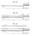
- FIG.3A-FIG.3C show section views of the image sensor
according to the first embodiment of the present invention in the
order of the manufacturing processes;
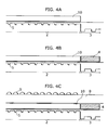
- FIG.4A-FIG.4C show section views of the image sensor
according to the second embodiment in the order of the
manufacturing processes;
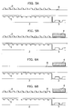
- FIG.5A and FIG.5B show section views of the image sensor
according to the third embodiment in the order of the manufacturing
processes;
- FIG.6A and FIG.6B show section views of the image sensor
according to the third embodiment in another order of the
manufacturing processes; and
- FIG.7A and 7B show section views of the image sensor
according to the fourth embodiment in the order of the
manufacturing processes.
-
DESCRIPTION OF THE PREFERRED EMBODIMENT(S)
(First Embodiment)
-
A sketchy top view of the image sensor according to the first
embodiment is the same as FIG.1, and comprises an imaging area2
including a plurality of pixel units (photodiode5), a wiring area3, and
a lightproof film4 on the wiring area3.
-
In the manufacturing method of the image sensor according to
the first embodiment, a transparent film10 is formed on the imaging
area2 using a material capable of patterning and of the same
thickness as an anti-flare pattern, either before or after the
anti-flare pattern of low transmittance (lightproof film4) is formed
on the wiring area3. In the formations of the transparent film10
and the lightproof film4, the height is made even between the top
surface of the transparent film10 and that of the lightproof film4.
The micro lenses are formed after a transparent film such as acryl is
applied. Consequently, a step height caused by the anti-flare
pattern (lightproof film4) is eliminated, thus the image sensor of low
shading can be manufactured.
-
FIG.3A-FIG.3C show section views of the image sensor
according to the first embodiment in the order of the manufacturing
processes. The manufacturing processes according to the present
embodiment will be explained in the order of (101) - (106) as
following:
- (101) After the wiring area3 and the imaging area2 are formed,
a transparent film is formed on the wiring area3 and the imaging
area2 so as to make a flat film over the wiring area3 and the imaging
area2. This formation of the transparent film is performed, for
example, by applying a transparent film, exposing it to light, and
developing it.
- (102) As shown in FIG.3A, a colorable photoresist4 of the same
thickness (0.3-0.9 µm) as the transparent film described above is
formed on the wiring area3. This formation is also performed by
patterning, that is, by applying the colorable photoresist4 of 0.3-0.9
µm, exposing it to light, and developing it.
- (103) As shown in FIG.3B, the colorable photoresist4 is colored
black, said photoresist4 being formed on the wiring area3, thereby
the photoresist4 is formed as the lightproof film4 (antireflective
film).
- (104) As shown in FIG.3B, the transparent film10 is formed,
using a material capable of patterning, on the imaging area2
covered with the flattening transparent film. As a material capable
of patterning, there is, for example, phenol type resin. Since acryl
resin is not capable of patterning in general, it is not used here.
The formation of this transparent film10 is performed by applying
the material capable of patterning, exposing it to light, and
developing it. In other words, (i) the material capable of
patterning is applied (0.3-0.9 µm) all over the top surface of the
imaging area2 covered with the flattening transparent film; ii) the
transparent film10 is exposed to light using a mask which covers
only the imaging area2, not the wiring area3 in the case the material
capable of patterning is a negative type; and iii) the area which was
uncovered with the mask (the exposed area) is eliminated by
developing the transparent film10. In the case the material
capable of patterning is a positive type, the transparent film10 is
exposed to light using a mask which covers only the wiring area3,
not the imaging area2; thereby, the area which was covered with the
mask (the unexposed area) is eliminated by developing the
transparent film10. In the processes of (102) and (104), in the
case a photoresist of the opposite characteristic is used, it is
possible to conduct the two processes with only one mask.
- (105) As shown in FIG.3C, the flat film(the transparent film8)
for forming micro lenses on top is applied (0.3-5.0 µm ). The
transparent film can be acryl.
- (106) As shown in FIG.3C, micro lenses9 are formed.
-
-
According to the image sensor manufactured by such processes
as described above, it is possible to pattern each of the lightproof
film4 over the wiring area3 and the transparent film10 over the
imaging area2; thus, it is possible to make the height even between
the top surface of the transparent film10 and that of the
antireflective film4. Consequently, it possible to manufacture the
image sensor of low shading which has less uneven sensitivity than
the conventional image sensor although it includes the antireflective
film (lightproof film4) for avoiding flares.
(Variation1)
-
The manufacturing processes according to the variation1 of
such manufacturing method as described above will be explained in
the order of (201) - (205). However, the same processes will be
omitted and the different processes will be mainly explained.
- (201) The wiring area3 is flattened in the same manner as
(101).
- (202) As shown in FIG.3A, the black photoresist4 (Black) for
controlling reflections is formed on the wiring area3 by applying the
black photoresist4 of 0.3-0.9 µm, exposing it to light, and developing
it. Thus, the black photoresist4 (Black) is formed as the
antireflective film. The photoresist can be either of a negative type
or a positive type.
- (203) As shown in FIG.3B, the transparent film10 is formed in
the area where Black does not exist by applying the transparent
film10 of 0.3-0.9 µm, exposing it to light, and developing it. The
sensitivity characteristic of the transparent film10 can be either of a
negative type or a positive type. In the case the photoresist of
Black is a positive type and the transparent film10 is a negative type,
it is possible to conduct two processes with one mask; and vice
versa.
- (204) As shown in FIG.3C, on Black and the transparent film10,
the flat film (the transparent film8) for forming micro lenses on top
is applied (0.3-5.0 µm).
- (205) The micro lenses are formed on the transparent film8.
-
(Variation2)
-
In addition, the manufacturing processes according to the
variation2 of such manufacturing method as described above will be
explained in the order of (301) - (306). However, the same
processes will be omitted and the different processes will be mainly
explained.
- (301) The wiring area3 is flattened in the same manner as
(101).
- (302) The blue or red photoresist (Blue or Red) is formed on the
wiring area3 by applying the blue or red photoresist of 0.3-0.9 µm,
exposing it to light, and developing it. The photoresist can be
either of a negative type or a positive type. Thus, about the lower
half of the antireflective film4 of FIG.3A is formed.
- (303) On the blue or red photoresist, another red or blue
photoresist (Red or Blue) is formed by applying the red or blue
photoresist of 0.3-0.9 um, exposing it to light, and developing it.
The photoresist can be either of a negative type or a positive type.
Thus, about the upper half of the antireflective film4 of FIG.3A is
formed.
- (304) On the imaging area2, the transparent film10 is formed
by applying the transparent film of the same thickness as the
combined blue and red photoresists, exposing it to light, and
developing it. The sensitivity characteristic of the transparent
film10 can be either of a negative type or a positive type. In the
case the photoresist of Red and Blue is a positive type and the
transparent film10 is a negative type, it is possible to conduct two
processes with one mask; and vice versa.
- (305) As shown in FIG.3C, on Red and Blue and the transparent
film10, the flat film (the transparent film8) for forming micro lenses
on top is applied (0.3-5.0 µm).
- (306) The micro lenses9 are formed on the transparent film8.
-
(Variation3)
-
Finally, the manufacturing processes according to the
variation3 of such manufacturing method as described above will be
explained in the order of (401) - (408). However, the same
processes will be omitted and the different processes will be mainly
explained.
- (401) The wiring area3 is flattened in the same manner as
(101).
- (402) The colorable photoresist is formed on the wiring area3
by applying it (0.3-0.9 µm), exposing it to light, and developing it.
The photoresist can be either of a negative type or a positive type.
Thus, about the lower half of the antireflective film4 as in FIG.3A is
formed.
- (403) The colorable photoresist is colored blue (or red).
- (404) On the blue (or red) photoresist, another colorable
photoresist is formed by applying it (0.3-0.9 µm), exposing it to light,
and developing it. The photoresist can be either of a negative type
or a positive type.
- (405) The colorable photoresist is colored red (or blue). Thus,
about the upper half of the antireflective film4 as in FIG.3A is
formed.
- (406) On the imaging area2, the transparent film10 is formed
by applying the transparent film of the same thickness (0.6-1.8 µm)
as the combined blue and red photoresists (Blue and Red), exposing
it to light, and developing it. The sensitivity characteristic of the
transparent film10 can be either of a negative type or a positive type.
In the case the photoresist of Red and Blue is a positive type and the
transparent film10 is a negative type, it is possible to conduct two
processes with one mask; and vice versa.
- (407) As shown in FIG.3C, on Red and Blue and the transparent
film10, the flat film(the transparent film8) for forming micro lenses
on top is applied (0.3-5.0 µm).
- (408) The micro lenses9 are formed on the transparent film8.
-
(Second Embodiment)
-
FIG.4A-FIG.4C show section views of the image sensor
according to the second embodiment in the order of the
manufacturing processes. While the transparent film10 is formed
after the formation of the lightproof film4 according to the
manufacturing method in FIG.3, the lightproof film4 is formed after
the formation of the transparent film10 in FIG.4.
-
The manufacturing processes according to the second
embodiment will be explained in the order of (101a) - (106a) as
following. However, the same processes as the first embodiment
will be omitted, and the different processes will be mainly explained.
- (101a) The wiring area3 is flattened in the same manner as
(101).
- (102a) The transparent film10 is formed on the imaging area2
in the same manner as (104). FIG.4A is a section view of this
formation.
- (103a) The colorable photoresist of the same thickness
(0.3-0.9 µm) as the transparent film is formed on the wiring area in
the same manner as (102).
- (104a) The colorable photoresist is colored black in the same
manner as (103). FIG.4B is a section view of this formation. Thus,
the lightproof film4 (the antireflective film) is formed.
- (105a) The flat film (the transparent film8) for forming micro
lenses on top is applied (0.3-5.0 µm) in the same manner as (105).
- (106a) The micro lenses9 are formed in the same manner as
(106). FIG.4C is a section view of this formation.
-
-
According to the image sensor manufactured by such processes
as described above, it is possible to form each of the lightproof film4
over the wiring area3 and the transparent film10 over the imaging
area2; thus, it is possible to make the height even between the top
surface of the transparent film10 and that of the antireflective film4.
Consequently, it possible to manufacture the image sensor of low
shading which has less uneven sensitivity than the conventional
image sensor although it includes the antireflective film (lightproof
film4) for avoiding flares.
-
The variations4-6 of the manufacturing method according to
the present embodiment will be explained as following. The
variations4-6 are performed according to the manufacturing method
in which the order of the formations of the lightproof film4 and the
transparent film10 is reversed from that of the variationsl-3
according to the first embodiment as mentioned above. In other
words, in the variations4-6, the lightproof film4 is formed after the
transparent film10 in the same manner as the variations1-3.
(Third Embodiment)
-
FIG.5A-FIG.5B show section views of the image sensor
according to the third embodiment in the order of the manufacturing
processes. The manufacturing processes according to the third
embodiment will. be explained in the order of (901) - (905) as
following.
- (901) The wiring area3 is flattened in the same manner as
(101).
- (902) The flat film(the transparent film8) for forming micro
lenses on top is applied (0.3-5.0 µm).
- (903) The micro lenses9 are formed. FIG.5A is a section view
of this formation.
- (904) Over the wiring area3, the colorable photoresist is
formed by applying it (0.3-0.9 µm), exposing it to light, and
developing it. The photoresist can be either of a negative type or a
positive type.
- (905) The colorable photoresist is colored black (Black). Thus,
the lightproof film4 is formed. FIG.5B shows the section view of
this formation.
-
-
In this manner, the lightproof film4 is formed on the flat film
(the transparent film8) for forming micro lenses on top, thereby this
formation prevents the step height from occurring among the micro
lenses due to the lightproof film4. In other words, the flat film
including the micro lenses on top is evenly formed over the imaging
area2 and the wiring area3. Consequently, it is possible to
manufacture the image sensor of low shading which has less uneven
sensitivity than the conventional image sensor.
-
The flat film (the transparent film8) is formed over the imaging
area2 and the wiring area3. However, as long as the transparent
film8 is formed over the imaging area2, the same effects can be
acquired.
-
The manufacturing processes according to the variation1 of the
third embodiment will be explained in the order of (111) - (114) as
following. However, the same processes will be omitted and the
different processes will be mainly explained.
- (111) The wiring area3 is flattened in the same manner as
(101).
- (112) The flat film(the transparent film8) for forming micro
lenses on top is applied (0.3-5.0 µm; depending on the cell size).
- (113) The micro lenses9 are formed. FIG.5A shows the
section view of this formation.
- (114) Over the wiring area3, the black photoresist (Black) is
patterned by applying it (0.3-0.9 µm ), exposing it to light, and
developing it. The photoresist can be either of a negative type or a
positive type. Thus, the lightproof film4 is formed. FIG.5B shows
the section view of this formation.
-
-
The manufacturing processes according to the variation2 of the
third embodiment will be explained in the order of (121) - (124) as
following. However, the same processes will be omitted and the
different processes will be mainly explained.
- (121) The wiring area3 is flattened in the same manner as
(101).
- (122) The flat film (the transparent film8) for forming micro
lenses on top is applied in the same manner as (112).
- (123) The micro lenses9 are formed in the same manner as
(113). FIG.5A shows the section view of this formation.
- (124) On the wiring area3, the red photoresist (Red) is formed
by applying it (0.3-0.9 µm), exposing it to light, and developing it.
The photoresist can be either of a negative type or a positive type.
- (125) On Red, the blue photoresist (Blue) is formed by applying
it (0.3-0.9 µm), exposing it to light, and developing it. The
photoresist can be either of a negative type or positive type.
FIG.5B shows the section view of this formation.
-
-
The manufacturing processes according to the variation3 of the
third embodiment will be explained in the order of (131) - (134) as
following. However, the same processes will be omitted and the
different processes will be mainly explained.
- (131) The wiring area3 is flattened in the same manner as
(101).
- (132) The flat film (the transparent film8) for forming micro
lenses on top is applied in the same manner as (112).
- (133) The micro lenses9 are formed on the transparent film8 in
the same manner as (113). FIG.5A shows the section view of this
formation.
- (134) The colorable photoresist is formed on the wiring area3
by applying it (0.3-0.9 µm), exposing it to light, and developing it.
The photoresist can be either of a negative type or a positive type.
- (135) The colorable photoresist is colored red (or blue).
- (136) On the red (or blue) photoresist, another colorable
photoresist is formed by applying it (0.3-0.9 µm), exposing it to light;
and developing it. The photoresist can be either of a negative type
or a positive type.
- (137) The colorable photoresist is colored blue (or red).
-
-
The image sensor as shown in FIG.5B can be manufactured
according to such variations as described above.
-
The manufacturing method of the image sensor as shown in
FIG.5B according to the processes of FIG.6A and FIG.6B will be
explained as following. While the lightproof film4 is formed after
the formation of the micro lenses in the manufacturing processes of
FIG.5, the lightproof film4 is formed before the formation of the
micro lenses in the manufacturing processes of FIG.6.
-
The manufacturing processes of FIG.6 will be explained in the
order of (901a) - (905a) as following. However, the same
processes will be omitted and the different processes will be mainly
explained.
- (901a) The wiring area3 is flattened in the same manner as
(901).
- (902a) The flat film(the transparent film8) for forming micro
lenses on top is applied (0.3-5.0 µm) in the same manner as (902).
- (903a) On the wiring area3, the colorable photoresist is formed
by applying it (0.3-0.9 µm), exposing it to light, and developing it in
the same manner as (904). The photoresist can be either of a
negative type or a positive type.
- (904a) The colorable photoresist is colored black (Black) in the
same manner as (905). Thus, the lightproof film4 is formed.
FIG.6A shows the section view of this formation.
- (905a) The micro lenses9 are formed in the same manner as
(903). FIG.6B is a section view of this formation (the same as
FIG.5B).
-
-
As described above, the order of the formations of the micro
lenses and the lightproof film4 is reversed between the
manufacturing processes of FIG.5A - FIG.5B and those of
FIG.6A-FIG.6B. However, it is possible to manufacture the image
sensor comprising the flat film (the transparent film8) which has an
evenly flat top surface for forming micro lenses on top according to
both of the manufacturing processes.
-
In the variations4-6 of the third embodiment, the order of the
formations of the micro lenses and the lightproof film4 is reversed
from that of the variations1-3 of the third embodiment.
(Fourth Embodiment)
-
FIG.7A-FIG.7B show the section views of the image sensor
according to the fourth embodiment in the order of the
manufacturing processes. The manufacturing processes of the
present embodiment will be explained in the order of (501) - (505).
- (501) Right on the wiring area3, the colorable photoresist is
formed by applying it (0.3-0.9 µm), exposing it to light, and
developing it so as to flatten the top surface of the wiring area3.
The photoresist can be either of a negative type or a positive type.
- (502) The colorable photoresist is colored black (Black). Thus,
the lightproof film4 is formed. FIG.7A shows the section view of
this formation.
- (503) On Black and the imaging area2, the flat film (the
transparent film8) for forming micro lenses on top is formed
(0.3-5.0 µm).
- (504) The micro lenses are formed. FIG.7B shows the section
view of this formation.
-
-
As described above, according to the image sensor of the fourth
embodiment, i) the lightproof film4 is formed to fill the gap between
the pixel units of the imaging area2 and the wiring area3; ii) the
transparent film8 is formed to flatten the top surface of the imaging
area2 and the wiring area3 covered with the lightproof film4; and iii)
the micro lenses9 are formed on the transparent film8. In this
manner, the flat film (the transparent film8) for forming micro
lenses on top is easily flattened. Consequently, it is possible to
manufacture the image sensor of low shading which has less uneven
sensitivity than the conventional image sensor.
-
The manufacturing processes according to the variation1 of the
fourth embodiment will be explained in the order of (601) - (603).
However, the same processes will be omitted and the different
processes will be mainly explained.
- (601) Right on the wiring area3, the black photoresist (Black)
for controlling reflections is formed by applying it (0.3-0.9 µm),
exposing it to light, and developing it. The photoresist can be
either of a negative type or a positive type.
- (602) On the imaging area2 and the wiring area3 covered with
Black, the flat film (the transparent film8) for forming micro lenses
on top is formed (0.3-5.0 µm). FIG.7A shows the section view of this
formation.
- (603) The micro lenses9 are formed on the transparent film8.
FIG.7B shows the section view of this formation.
-
-
The manufacturing processes according to the variation2 of the
fourth embodiment will be explained in the order of (701) - (704).
However, the same processes will be omitted and the different
processes will be mainly explained.
- (701) Right on the wiring area3, the red (or blue) photoresist is
formed by applying it (0.3-0.9 µm ), exposing it to light, and
developing it. The photoresist can be either of a negative type or a
positive type.
- (702) On
the red (or blue) photoresist, another blue (or red) photoresist is
formed by applying it (0.3-0.9 µm), exposing it to light, and
developing it. The photoresist can be either of a negative type or a
positive type.
- (703) On the imaging area2 and the wiring area3 covered with
the red and blue photoresists, the flat film(the transparent film8) for
forming micro lenses on top is formed (0.3-5.0 µm). FIG.7A shows
the section view of this formation.
- (704) The micro lenses9 are formed. FIG.7B shows the
section view of this formation.
-
-
The manufacturing processes according to the variation3 of the
fourth embodiment will be explained in the order of (801) - (806).
However, the same processes will be omitted and the different
processes will be mainly explained.
- (801) Right on the wiring area3, the colorable photoresist is
formed by applying it (0.3-0.9 µm ), exposing it to light, and
developing it. The photoresist can be either of a negative type or a
positive type.
- (802) The colorable photoresist is colored red (or blue).
- (803) On the red (or blue) photoresist, another colorable
photoresist is formed by applying it (0.3-0.9 µm) , exposing it to light,
and developing it. The photoresist can be either of a negative type
or a positive type.
- (804) The colorable photoresist is colored blue (or red).
- (805) On the imaging area2 and the wiring area3 covered with
the red and blue photoresists, the flat film (the transparent film8)
for forming micro lenses on top is formed (0.3-5.0 µm). FIG.7A
shows the section view of this formation.
- (806) The micro lenses9 are formed. FIG.7B shows the
section view of this formation.
-
-
The image sensor as shown in FIG.7B can be manufactured
according to such variations as described above.
-
Although the present invention has been fully described by way
of examples with reference to the accompanying drawings, it is to be
noted that various changes and modifications will be apparent to
those skilled in the art. Therefore, unless otherwise such changes
and modifications depart from the scope of the present invention,
they should be construed as being included therein.