EP1486817A1 - Method of manufacturing optical modulator - Google Patents
Method of manufacturing optical modulator Download PDFInfo
- Publication number
- EP1486817A1 EP1486817A1 EP03710447A EP03710447A EP1486817A1 EP 1486817 A1 EP1486817 A1 EP 1486817A1 EP 03710447 A EP03710447 A EP 03710447A EP 03710447 A EP03710447 A EP 03710447A EP 1486817 A1 EP1486817 A1 EP 1486817A1
- Authority
- EP
- European Patent Office
- Prior art keywords
- substrate
- thin
- wall portion
- optical modulator
- machining process
- Prior art date
- Legal status (The legal status is an assumption and is not a legal conclusion. Google has not performed a legal analysis and makes no representation as to the accuracy of the status listed.)
- Granted
Links
Images



Classifications
-
- G—PHYSICS
- G02—OPTICS
- G02F—OPTICAL DEVICES OR ARRANGEMENTS FOR THE CONTROL OF LIGHT BY MODIFICATION OF THE OPTICAL PROPERTIES OF THE MEDIA OF THE ELEMENTS INVOLVED THEREIN; NON-LINEAR OPTICS; FREQUENCY-CHANGING OF LIGHT; OPTICAL LOGIC ELEMENTS; OPTICAL ANALOGUE/DIGITAL CONVERTERS
- G02F1/00—Devices or arrangements for the control of the intensity, colour, phase, polarisation or direction of light arriving from an independent light source, e.g. switching, gating or modulating; Non-linear optics
- G02F1/01—Devices or arrangements for the control of the intensity, colour, phase, polarisation or direction of light arriving from an independent light source, e.g. switching, gating or modulating; Non-linear optics for the control of the intensity, phase, polarisation or colour
- G02F1/21—Devices or arrangements for the control of the intensity, colour, phase, polarisation or direction of light arriving from an independent light source, e.g. switching, gating or modulating; Non-linear optics for the control of the intensity, phase, polarisation or colour by interference
- G02F1/225—Devices or arrangements for the control of the intensity, colour, phase, polarisation or direction of light arriving from an independent light source, e.g. switching, gating or modulating; Non-linear optics for the control of the intensity, phase, polarisation or colour by interference in an optical waveguide structure
-
- G—PHYSICS
- G02—OPTICS
- G02F—OPTICAL DEVICES OR ARRANGEMENTS FOR THE CONTROL OF LIGHT BY MODIFICATION OF THE OPTICAL PROPERTIES OF THE MEDIA OF THE ELEMENTS INVOLVED THEREIN; NON-LINEAR OPTICS; FREQUENCY-CHANGING OF LIGHT; OPTICAL LOGIC ELEMENTS; OPTICAL ANALOGUE/DIGITAL CONVERTERS
- G02F1/00—Devices or arrangements for the control of the intensity, colour, phase, polarisation or direction of light arriving from an independent light source, e.g. switching, gating or modulating; Non-linear optics
- G02F1/01—Devices or arrangements for the control of the intensity, colour, phase, polarisation or direction of light arriving from an independent light source, e.g. switching, gating or modulating; Non-linear optics for the control of the intensity, phase, polarisation or colour
- G02F1/21—Devices or arrangements for the control of the intensity, colour, phase, polarisation or direction of light arriving from an independent light source, e.g. switching, gating or modulating; Non-linear optics for the control of the intensity, phase, polarisation or colour by interference
- G02F1/225—Devices or arrangements for the control of the intensity, colour, phase, polarisation or direction of light arriving from an independent light source, e.g. switching, gating or modulating; Non-linear optics for the control of the intensity, phase, polarisation or colour by interference in an optical waveguide structure
- G02F1/2255—Devices or arrangements for the control of the intensity, colour, phase, polarisation or direction of light arriving from an independent light source, e.g. switching, gating or modulating; Non-linear optics for the control of the intensity, phase, polarisation or colour by interference in an optical waveguide structure controlled by a high-frequency electromagnetic component in an electric waveguide structure
-
- G—PHYSICS
- G02—OPTICS
- G02F—OPTICAL DEVICES OR ARRANGEMENTS FOR THE CONTROL OF LIGHT BY MODIFICATION OF THE OPTICAL PROPERTIES OF THE MEDIA OF THE ELEMENTS INVOLVED THEREIN; NON-LINEAR OPTICS; FREQUENCY-CHANGING OF LIGHT; OPTICAL LOGIC ELEMENTS; OPTICAL ANALOGUE/DIGITAL CONVERTERS
- G02F2203/00—Function characteristic
- G02F2203/21—Thermal instability, i.e. DC drift, of an optical modulator; Arrangements or methods for the reduction thereof
-
- Y—GENERAL TAGGING OF NEW TECHNOLOGICAL DEVELOPMENTS; GENERAL TAGGING OF CROSS-SECTIONAL TECHNOLOGIES SPANNING OVER SEVERAL SECTIONS OF THE IPC; TECHNICAL SUBJECTS COVERED BY FORMER USPC CROSS-REFERENCE ART COLLECTIONS [XRACs] AND DIGESTS
- Y10—TECHNICAL SUBJECTS COVERED BY FORMER USPC
- Y10T—TECHNICAL SUBJECTS COVERED BY FORMER US CLASSIFICATION
- Y10T29/00—Metal working
- Y10T29/49—Method of mechanical manufacture
- Y10T29/49002—Electrical device making
-
- Y—GENERAL TAGGING OF NEW TECHNOLOGICAL DEVELOPMENTS; GENERAL TAGGING OF CROSS-SECTIONAL TECHNOLOGIES SPANNING OVER SEVERAL SECTIONS OF THE IPC; TECHNICAL SUBJECTS COVERED BY FORMER USPC CROSS-REFERENCE ART COLLECTIONS [XRACs] AND DIGESTS
- Y10—TECHNICAL SUBJECTS COVERED BY FORMER USPC
- Y10T—TECHNICAL SUBJECTS COVERED BY FORMER US CLASSIFICATION
- Y10T29/00—Metal working
- Y10T29/49—Method of mechanical manufacture
- Y10T29/49002—Electrical device making
- Y10T29/49016—Antenna or wave energy "plumbing" making
-
- Y—GENERAL TAGGING OF NEW TECHNOLOGICAL DEVELOPMENTS; GENERAL TAGGING OF CROSS-SECTIONAL TECHNOLOGIES SPANNING OVER SEVERAL SECTIONS OF THE IPC; TECHNICAL SUBJECTS COVERED BY FORMER USPC CROSS-REFERENCE ART COLLECTIONS [XRACs] AND DIGESTS
- Y10—TECHNICAL SUBJECTS COVERED BY FORMER USPC
- Y10T—TECHNICAL SUBJECTS COVERED BY FORMER US CLASSIFICATION
- Y10T29/00—Metal working
- Y10T29/49—Method of mechanical manufacture
- Y10T29/49002—Electrical device making
- Y10T29/49082—Resistor making
- Y10T29/49085—Thermally variable
-
- Y—GENERAL TAGGING OF NEW TECHNOLOGICAL DEVELOPMENTS; GENERAL TAGGING OF CROSS-SECTIONAL TECHNOLOGIES SPANNING OVER SEVERAL SECTIONS OF THE IPC; TECHNICAL SUBJECTS COVERED BY FORMER USPC CROSS-REFERENCE ART COLLECTIONS [XRACs] AND DIGESTS
- Y10—TECHNICAL SUBJECTS COVERED BY FORMER USPC
- Y10T—TECHNICAL SUBJECTS COVERED BY FORMER US CLASSIFICATION
- Y10T29/00—Metal working
- Y10T29/49—Method of mechanical manufacture
- Y10T29/49002—Electrical device making
- Y10T29/49117—Conductor or circuit manufacturing
-
- Y—GENERAL TAGGING OF NEW TECHNOLOGICAL DEVELOPMENTS; GENERAL TAGGING OF CROSS-SECTIONAL TECHNOLOGIES SPANNING OVER SEVERAL SECTIONS OF THE IPC; TECHNICAL SUBJECTS COVERED BY FORMER USPC CROSS-REFERENCE ART COLLECTIONS [XRACs] AND DIGESTS
- Y10—TECHNICAL SUBJECTS COVERED BY FORMER USPC
- Y10T—TECHNICAL SUBJECTS COVERED BY FORMER US CLASSIFICATION
- Y10T29/00—Metal working
- Y10T29/49—Method of mechanical manufacture
- Y10T29/49002—Electrical device making
- Y10T29/49117—Conductor or circuit manufacturing
- Y10T29/49124—On flat or curved insulated base, e.g., printed circuit, etc.
- Y10T29/49126—Assembling bases
Definitions
- the present invention relates to a method of manufacturing an optical modulator suitable for use in a high-speed, large-capacity optical fiber communication system or the like.
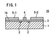
- FIG. 1 is a cross-sectional view of a conventional optical modulator.
- the optical modulator 10 shown in FIG. 1 has coplanar waveguide (CPW) modulation electrodes for modulating light guided through an optical waveguide.
- the optical modulator 10 comprises a substrate 1 in the form of an X-cut plate of lithium niobate, Mach-Zehnder optical waveguides 2 formed directly beneath a principal surface IA of the substrate 1 by titanium diffusion, a buffer layer 3 of silicon oxide formed on the principal surface IA, and a central electrode 4 and ground electrodes 5-1, 5-2 formed on the buffer layer 3.
- CPW coplanar waveguide
- FIG. 2 is a cross-sectional view of another conventional optical modulator.
- the optical modulator 20 shown in FIG. 2 has coplanar waveguide (CPW) modulation electrodes for modulating light guided through an optical waveguide.
- the optical modulator 20 comprises a substrate 11 in the form of an Z-cut plate of lithium niobate, Mach-Zehnder optical waveguides 12 formed directly beneath a principal surface 11A of the substrate 11 by titanium diffusion, a buffer layer 13 of silicon oxide formed on the principal surface 11A, and a central electrode 14 and ground electrodes 15-1, 15-2 formed on the buffer layer 13.
- the buffer layers 3, 13 are provided for the purpose of increasing speed matching between the light guided through the optical waveguides 2, 12 and a microwave applied to the modulating electrodes.
- the buffer layers 3, 13 included in the substrates 1, 11 are responsible for a DC drift that is produced. Furthermore, since modulation signals are applied from the modulation electrodes through the buffer layers 3, 13 to the light guided through the optical waveguides 2, 12, a substantial modulation signal voltage applied to the light is reduced. For effectively energizing the optical modulators 10, 20, it is necessary to apply a relatively high voltage to the modulation electrodes, despite the demand for reduced drive voltages.
- the optical modulator 20 shown in FIG. 2 since the optical waveguides 12 are positioned asymmetrically with respect to the central electrode 14, the chirp increases, failing to make long-distance transmission.
- the present invention provides a method of manufacturing an optical modulator having a novel arrangement which achieves speed matching without a buffer layer and which is free from the above problems.
- a method of manufacturing an optical modulator comprises the steps of forming an optical waveguide directly beneath a principal surface of a substrate made of a material having an electro-optic effect, forming modulation electrodes for modulating light guided through the optical waveguide, on the principal surface of the substrate, applying the principal surface of the substrate to a base substrate with the modulation electrodes interposed therebetween, performing a first machining process on a reverse side of the substrate while the base substrate is fixed in position, thereby processing the substrate in its entirety into a thin plate, performing a second machining process on the reverse side of the substrate, which is processed into a thin plate, to process a portion of the substrate which includes the optical waveguide into a thin-wall portion, performing a third machining process on the thin-wall portion of the substrate to process the portion of the substrate which includes the optical waveguide into a first thin-wall portion and to process a portion adjacent to the first thin-wall portion into a second thin-wall portion which is thinner than the first thin-wall portion, and applying the reverse side of the
- a method of manufacturing an optical modulator comprises the steps of forming an optical waveguide directly beneath a principal surface of a substrate made of a material having an electro-optic effect, forming modulation electrodes for modulating light guided through the optical waveguide, on the principal surface of the substrate, applying the principal surface of the substrate to a base substrate with the modulation electrodes interposed therebetween, performing a first machining process on a reverse side of the substrate while the base substrate is fixed in position, thereby processing the substrate in its entirety into a thin plate, performing a second machining process on the reverse side of the substrate which is processed into a thin plate to process a portion of the substrate which includes the optical waveguide into a thin-wall portion, performing a laser machining process on the thin-wall portion of the substrate to process the portion of the substrate which includes the optical waveguide into a first thin-wall portion and to process a portion adjacent to the first thin-wall portion into a second thin-wall portion which is thinner than the first thin-wall portion, and applying the reverse side of the substrate to
- a method of manufacturing an optical modulator comprises the steps of forming an optical waveguide directly beneath a principal surface of a substrate made of a material having an electro-optic effect, forming modulation electrodes for modulating light guided through the optical waveguide, on the principal surface of the substrate, applying the principal surface of the substrate to a base substrate with the modulation electrodes interposed therebetween, performing a first machining process on a reverse side of the substrate while the base substrate is fixed in position, thereby processing the substrate in its entirety into a thin plate, performing a laser machining process on the reverse side of the substrate which is processed into a thin plate to process a portion of the substrate which includes the optical waveguide into a thin-wall portion, performing a second machining process on the thin-wall portion of the substrate to process the portion of the substrate which includes the optical waveguide into a first thin-wall portion and to process a portion adjacent to the first thin-wall portion into a second thin-wall portion which is thinner than the first thin-wall portion, and applying the reverse side of the substrate to
- a method of manufacturing an optical modulator comprises the steps of forming an optical waveguide directly beneath a principal surface of a substrate made of a material having an electro-optic effect, forming modulation electrodes for modulating light guided through the optical waveguide, on the principal surface of the substrate, applying the principal surface of the substrate to a base substrate with the modulation electrodes interposed therebetween, performing a machining process on a reverse side of the substrate while the base substrate is fixed in position, thereby processing the substrate in its entirety into a thin plate, performing a first laser machining process on the reverse side of the substrate which is processed into a thin plate to process a portion of the substrate which includes the optical waveguide into a thin-wall portion, performing a second laser machining process on the thin-wall portion of the substrate to process the portion of the substrate which includes the optical waveguide into a first thin-wall portion and to process a portion adjacent to the first thin-wall portion into a second thin-wall portion which is thinner than the first thin-wall portion, and applying the reverse side of the substrate
- the inventors have succeeded in developing an optical modulator having a novel arrangement which is capable of achieving speed matching without a buffer layer and reducing a coupling loss that is caused when an optical fiber is coupled.
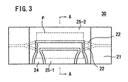
- FIG. 3 is a plan view of a novel optical modulator manufactured by a manufacturing method according to the present invention
- FIG. 4 is a cross-sectional view taken along line A - A of FIG. 3.
- the optical modulator 30 shown in FIGS. 3 and 4 comprises a thin substrate 21 made of a material having an electro-optic effect, such as lithium niobate, Mach-Zehnder optical waveguides 22 formed in the substrate 21 near a principal surface 21A thereof, and a central electrode 24 and ground electrodes 25-1, 25-2 formed on the substrate 21.
- the central electrode 24 and the ground electrodes 25-1, 25-2 serve as CPW modulation electrodes for modulating light guided through optical waveguides 22.
- the reverse side of the substrate 21 is processed to provide a first thin-wall portion 26 formed in a region including the optical waveguides 22, and second thin-wall portions 27 formed adjacent to the first thin-wall portion 26, the second thin-wall portions 27 being thinner than the first thin-wall portion 26.
- the first thin-wall portion 26 has an end face (reverse side) positioned directly beneath the optical waveguides 22.
- modulation signals from the modulation electrodes seep into a low-dielectric-constant region (air) that is present below the second thin-wall portion 27, speed matching conditions can be satisfied without forming a buffer layer. Furthermore, because the modulation signals are effectively applied to the optical waveguides 22, a drive voltage applied to the optical modulator 30 is lowered.
- the first thin-wall portion 26 formed in the region including the optical waveguides 22 has a thickness t1 greater than the thickness t2 of the second thin-wall portions 27 formed adjacent to the first thin-wall portion 26. Therefore, the optical waveguides 22 have a cross-sectional shape prevented from being flattened. Consequently, when light is applied, any reduction in a coupling loss with respect to a region where the first and second thin-wall portions 26, 27 are not formed is prevented.
- the first and second thin-wall portions 26, 27 should preferably be formed coextensively with a region P shown in FIG. 3.
- the region P is a region where light guided through the optical waveguides 22 and modulation signals from the modulation electrodes substantially coact with each other, and a region indicated by the broken lines where the optical waveguides 22, the central electrode 24, and the ground electrodes 25-1, 25-2 extend substantially parallel to each other.
- the first thin-wall portion 26 and the second thin-wall portion 27 may be formed so as to include the region P and extend entirely along the optical waveguides 22 of the substrate 21.
- the substrate 21 since the substrate 21 is thin and has the first thin-wall portion 26 and the second thin-wall portion 27, the substrate 21 may not be of sufficient mechanical strength. Therefore, a support substrate 31 made of lithium niobate or the like is applied to a reverse side 21B of the substrate 21.
- FIG. 5 is a cross-sectional view of a modification of the optical modulator shown in FIGS. 3 and 4.
- An optical modulator 40 shown in FIG. 5 is basically of the same structure as the optical modulator 30 shown in FIGS. 3 and 4, but differs therefrom in that a groove 35 is defined in the support substrate 31, and the reverse side 21B of the substrate 21 is applied to a principal surface 31A of the support substrate 31 such that the optical waveguides 22, the first thin-wall portion 26, and the second thin-wall portions 27 are positioned within the groove 35.
- the groove 28 has a depth d of 1 ⁇ m or more and preferably in the range from 10 ⁇ m to 200 ⁇ m.
- the substrate 21 is a thin plate from a substrate material having a thickness of some millimeters until the thickness Ts thereof is in the range from about 50 ⁇ m to 300 ⁇ m.
- the first thin-wall portion 26 has a small thickness t1 in the range from about 15 ⁇ m to 50 ⁇ m, and the second thin-wall portions t2 have a small thickness of 12.5 ⁇ m or less.
- machining techniques for producing thin plates and thin-wall portions are not yet sufficiently established, and the yield of such optical modulators is extremely low.
- the inventors have made intensive studies to establish machining techniques for realizing the above structures and to find a method of stably producing the optical modulators 30, 40 shown in FIGS. 3 and 4 and FIG. 5.
- the inventors have invented the first manufacturing method through the fourth manufacturing method described above, i.e., have found that after a substrate material is applied to a base substrate, the base substrate is fixed, the substrate material is machined into a substrate as a thin plate, and thin-wall portions are produced by machining or laser processing, resulting in an increase in the yield of optical modulators.
- FIGS. 6 through 10 are cross-sectional views showing the manufacturing steps of the manufacturing method according to the first embodiment.
- a plurality of optical modulators are simultaneously fabricated on a wafer (substrate) having a predetermined size.
- a wafer substrate having a predetermined size.
- one optical modulator fabricated on the wafer will be described.
- a predetermined mask pattern is formed on a principal surface 21A of a substrate 21 which is made of a material having an electro-optic effect, such as lithium niobate
- Mach-Zehnder optical waveguides 22 are fabricated directly beneath the principal surface 21A by titanium diffusion or the like.
- a predetermined mask pattern is formed on the principal surface 21A of the substrate 21, and CPW modulation electrodes comprising a central electrode 24 and ground electrodes 25-1, 25-2 are fabricated by plating or a combination of evaporation and plating.
- the central electrode 24 and the ground electrodes 25-1, 25-2 have a thickness Te preferably in the range from 15 ⁇ m to 50 ⁇ m, and the central electrode 24 has a width W preferably in the range from 5 ⁇ m to 50 ⁇ m, for thereby reducing an electrode loss of modulation signals.
- Gaps G between the central electrode 24 and the ground electrodes 25-1, 25-2 should preferably in the range from 25 ⁇ m to 55 ⁇ m for thereby suppressing an increase in the drive voltage and also effectively modulating light that is guided through the optical waveguides 22.
- the principal surface 21A of the substrate 21 is applied to a base substrate 41 by a thermoplastic resin 39 interposed therebetween, and the base substrate 41 is fixed to the level block of a polishing machine or the like by a thermoplastic resin.
- the reverse side 21B of the substrate 21 is subjected to a polishing process as a first machining process until the substrate 21 is polished to a thin plate having a thickness Ts.
- the thickness Ts of the substrate 21 is in the range from 30 ⁇ m to 300 ⁇ m.
- the polishing process comprises a lateral polishing process, a high-speed lapping process, and a chemical polishing process (CMP).
- a reverse side 21B of the substrate 21 is subjected to a second machining process to form a thin-wall portion 28.
- regions except regions including the optical waveguides 22 are subjected to a third machining process to form a first thin-wall portion 26 including the optical waveguides 22 and second thin-wall portions 27 disposed adjacent to the first thin-wall portion 26 and thinner than the first thin-wall portion 26, as shown in FIG. 10.
- Those regions of the first and second thin-wall portions 26, 27 which correspond to portions other than the CPW electrodes are not machined. Therefore, since the first and second thin-wall portions 26, 27 are covered with a thick substrate portion, their mechanical strength is maintained.
- the first machining process and the second machining process are performed after the base substrate 41 is fixedly applied by a thermoplastic resin to the level block of a grinding machine such as a microgrinder, sand blaster, or the like.
- the first thin-wall portion 26 has a thickness t1 preferably in the range from 5 ⁇ m to 30 ⁇ m for preventing the optical waveguides 22 from being flattened to suppress an increase in the coupling loss that is caused when an optical fiber is coupled and to effectively apply modulating electrodes from the modulation electrodes to light guided through the optical waveguides 22.
- the first thin-wall portion 26 has a width L preferably in the range from (W + 2 ⁇ m) to (W + 2G) where W is the width of the central electrode 24 and G is the gap between the first and second thin-wall portions 26, 27.
- the second thin-wall portions 27 have a thickness t2 required to be smaller than the thickness t1 of the first thin-wall portion, preferably to meet the relationship t1 - t2 ⁇ 1 ⁇ m, for thereby effectively applying modulating signals from the modulation electrodes to light guided through the optical waveguides 22.
- the reverse side 21B of the substrate 21 and the principal surface 31A of the support substrate 31 are applied to each other by a thermoplastic resin such as epoxy film interposed therebetween, fabricating the optical modulator 30 shown in FIGS. 3 and 4 or the optical modulator 40 shown in FIG. 5. If the optical modulator 40 shown in FIG. 5 is fabricated, then the groove 35 is defined in the principal surface 31A of the support substrate 31, and the substrate 21 and the support substrate 31 are applied to each other such that the optical waveguides 22, the first thin-wall portion 26, and the second thin-wall portions 27 are positioned within the groove 35. Thereafter, the base substrate 41 is removed from the substrate 21.
- a thermoplastic resin such as epoxy film interposed therebetween
- the second machining process and the third machining process include a grinding process using a microgrinder.
- the outer circumferential blade of the microgrinder tends to be deformed and has its grinding surface suffering surface irregularities which are liable to introduce variations in the substrate thickness. Therefore, during the grinding process, it is preferable to perform, from time to time, truing on the grinding surface to keep the outer circumferential blade in shape. Since the shape of the outer circumferential blade reflects the surface accuracy of the truing tool, the truing tool should preferably be made of a material that has surface roughness or planarity that satisfies prescribed conditions and is harder than the outer circumferential blade of the microgrinder.
- the particle size and shape of the abrasive grain of the outer circumferential blade that is used may be selected appropriately.
- a wedge-shaped blade may be used in the second machining process to form wedge-shaped second thin-wall portions 27.
- the thickness of the tip ends of the wedge-shaped second thin-wall portions, i.e., the smallest thickness thereof, is represented by t1.
- the second thin-wall portions 27 thus formed are effective to prevent the substrate 21 from cracking and also to increase the mechanical strength of the substrate 21 and the mechanical strength of the optical modulator 30.
- the assembly of the optical modulator 30 is basically fabricated by the process shown in FIGS. 6 through 10, except as follows:
- regions except regions including the optical waveguides 22 are subjected to a laser machining process to form a first thin-wall portion 26 including the optical waveguides 22 and second thin-wall portions 27 disposed adjacent to the first thin-wall portion 26 and thinner than the first thin-wall portion 26.
- regions of the first and second thin-wall portions 26, 27 which correspond to portions other than the CPW electrodes are not machined.
- the laser machining process may be performed using an excimer laser having a pulse duration of 10 nsecs. or less, with an irradiation intensity set to a value in the range from 1 mJ to 2 mJ.
- the first thin-wall portion 26 and the second thin-wall portions 27 can thus be formed highly accurately in a relative short period of time.
- the reverse side 21B of the substrate 21 and the principal surface 31A of the support substrate 31 are applied to each other by a thermoplastic resin such as epoxy film interposed therebetween, fabricating the optical modulator 30 shown in FIGS. 3 and 4 or the optical modulator 40 shown in FIG. 5.
- the machining process used to form the thin-wall portion 28 shown in FIG. 9 is performed after the base substrate 41 is fixedly applied by a thermoplastic resin to the level block of a grinding machine such as a microgrinder, sand blaster, or the like.
- a grinding machine such as a microgrinder, sand blaster, or the like. The roughness and width of the blade used in the grinding process are selected appropriately.
- the machining process includes a grinding process using a microgrinder or the like. It is preferable to perform, from time to time, truing on the grinding surface to keep the outer circumferential blade in shape.
- the dimensions required on the optical modulator 30 including the substrate 21 as a thin plate and the first thin-wall portion 26 and the second thin-wall portions 27 are the same as those in the first manufacturing process.
- the assembly of the optical modulator 30 is basically fabricated by the process shown in FIGS. 6 through 10, except as follows:
- the thin-wall portion 28 shown in FIG. 9 is fabricated by a laser machining process instead of the grinding process described above.
- the laser machining process may be performed using an excimer laser, with an irradiation intensity set to a value in the range from 1.0 J/cm 2 to 8.0 J/cm 2 .
- the thin-wall portion 28 can thus be formed highly accurately in a relative short period of time.
- the thin-wall portion 28 is subjected to a machining process which is the same as the second machining process in the manufacturing process according to the first embodiment to form a first thin-wall portion 26 including the optical waveguides 22 and second thin-wall portions 27 disposed adjacent to the first thin-wall portion 26 and thinner than the first thin-wall portion 26, as shown in FIG. 10.
- a machining process which is the same as the second machining process in the manufacturing process according to the first embodiment to form a first thin-wall portion 26 including the optical waveguides 22 and second thin-wall portions 27 disposed adjacent to the first thin-wall portion 26 and thinner than the first thin-wall portion 26, as shown in FIG. 10.
- end faces directly beneath the optical waveguides 22 are not machined.
- the machining process is performed after the base substrate 31 is fixedly applied by a thermoplastic resin to the level block of a grinding machine such as a microgrinder, sand blaster, or the like.
- a grinding machine such as a microgrinder, sand blaster, or the like.
- the roughness and width of the blade used in the grinding process are selected appropriately.
- a wedge-shaped blade may be used to form wedge-shaped second thin-wall portions 27, as shown in FIG. 11.
- the machining process includes a grinding process using a microgrinder or the like, in the same manner as described above. It is preferable to perform, from time to time, truing on the grinding surface to keep the outer circumferential blade in shape.
- the dimensions required on the optical modulator 30 including the substrate 21 as a thin plate and the first thin-wall portion 26 and the second thin-wall portions 27 are the same as those in the first manufacturing process.
- the assembly of the optical modulator 30 is basically fabricated by the process shown in FIGS. 6 through 10, except as follows:
- the thin-wall portion 28 shown in FIG. 10 is fabricated by a first laser machining process instead of the grinding process described above.
- the first thin-wall portion 26 and the second thin-wall portions 27 are fabricated by a second laser machining process performed on the thin-wall portion 28.
- the first laser machining process may be performed using an excimer laser, with an irradiation intensity set to a value in the range from 1.0 J/cm 2 to 8.0 J/cm 2 .
- the thin-wall portion 28 can thus be formed highly accurately in a relative short period of time.
- the second laser machining process may be performed using an excimer laser having a pulse duration of 10 nsecs. or less, with an irradiation intensity set to a value in the range from 1 mJ to 2 mJ.
- the first thin-wall portion 26 and the second thin-wall portions 27 can thus be formed highly accurately in a relative short period of time.
- the dimensions required on the optical modulator 30 including the substrate 21 as a thin plate and the first thin-wall portion 26 and the second thin-wall portions 27 are the same as those in the first manufacturing process.
- the optical modulator shown in FIGS. 3 and 4 was fabricated according to the process shown in FIGS. 6 through 10 based on the first manufacturing process.
- An X-cut plate of lithium niobate having a thickness of 0.5 mm was used as the substrate 21, and the Mach-Zehnder optical waveguides 22 were formed in the substrate 21 near the principal surface 21A thereof by titanium diffusion, as shown in FIG. 6.
- the CPW modulation electrodes were fabricated on the principal surface 21A by plating.
- the central electrode 24 had a width W of 30 ⁇ m, the gaps G between the central electrode 24 and the ground electrodes 25-1, 25-2 were each of 40 ⁇ m, and the electrodes had a thickness Te of 30 ⁇ m and a length of 40 mm.
- a resin-bonded blade of #6000 having a width of 100 ⁇ m was used to perform a machining process on the reverse side 21B of the substrate 21, forming the thin-wall portion 28 shown in FIG. 9.
- the blade had a rotational speed of 12000 rpm.
- the substrate was ground 1 ⁇ m from the surface thereof at a rate of 0.1 mm/min. in the thickness direction of the substrate, and then slotted at a rate of 20 mm/min. in the horizontal direction (in the direction of the electrode length) from that position. The above process was repeated to machine the substrate.
- truing was performed, using a grinding wheel of #1500 each time the substrate was machined 100 ⁇ m in the thickness direction.
- the first thin-wall portion 26 had a width L of 90 pm and a thickness t1 of 15 ⁇ m
- the second thin-wall portions 27 had a thickness t2 of 10 ⁇ m. The thicknesses of these thin-wall portions were measured by a shape measuring unit.
- An optical fiber was bonded to the optical modulator 30 by an UV-curable resin, and the packaged optical modulator was evaluated for S21 characteristics.
- the -6 dB band was 40 GHz and over, and the microwave effective refractive index nm was 2.15.
- the evaluated optical response for -3 dB was 40 GHz and over.
- the coupling loss was 5 dB.
- the optical modulator 30 was fabricated in the same manner as Example 1 except that the second machining process was performed using a wedge-shaped blade to form the wedge-shaped second thin-wall portions 27 shown in FIG. 11.
- the second thin-wall portions 27 had a thickness t2 of 10 ⁇ m, as with Example 1.
- the optical modulator 30 had the same S21 characteristics, optical response, and coupling loss as those of Example 1.
- the optical modulator 30 was fabricated in the same manner and of the same dimensions as Example 1 except that a laser machining process, instead of the second machining process, was performed on the thin-wall portion 28, and the first thin-wall portion 26 and the second thin-wall portions 27 were formed according to the second manufacturing method.
- the laser machining process was performed using a KrF excimer laser having a frequency of 120 Hz, with an irradiation intensity of 2 mJ and a scanning speed of 300 ⁇ m/sec.
- the optical modulator 30 had the same S21 characteristics, optical response, and coupling loss as those of Example 1.
- the optical modulator 30 was fabricated in the same manner and of the same dimensions as Example 1 except that a laser machining process, instead of the first machining process, was performed on the reverse side 21B of the substrate 21, and the thin-wall portion 28 was fabricated according to the third manufacturing method.
- the laser machining process was performed using a KrF excimer laser having a frequency of 195 Hz, with an irradiation intensity of 6.8 J/cm 2 and a scanning speed of 1800 ⁇ m/sec. After the substrate 21 was machined until its thickness reaches 100 ⁇ m, it was machined with an irradiation intensity of 3.8 J/cm 2 and a scanning speed of 1800 ⁇ m/sec. until its thickness reaches 15 ⁇ m.
- the optical modulator 30 had the same S21 characteristics, optical response, and coupling loss as those of Example 1.
- the optical modulator 30 was fabricated in the same manner and of the same dimensions as Example 1 except that a first laser machining process, instead of the first machining process, was performed to form the thin-wall portion 28, a second laser machining process, instead of the second machining process, was performed on the thin-wall portion 28, and the first thin-wall portion 26 and the second thin-wall portions 27 were formed according to the fourth manufacturing method.
- the first laser machining process was performed using a KrF excimer laser having a frequency of 195 Hz, with an irradiation intensity of 6.8 J/cm 2 and a scanning speed of 1800 ⁇ m/sec.
- the substrate 21 was machined until its thickness reaches 100 ⁇ m, it was machined with an irradiation intensity of 3.8 J/cm 2 and a scanning speed of 1800 ⁇ m/sec. until its thickness reaches 15 ⁇ m.
- the second laser machining process was performed using a KrF excimer laser having a pulse duration of 4 nsecs. and a frequency of 120 Hz, with an irradiation intensity of 2 mJ and a scanning speed of 300 ⁇ m/sec.
- the optical modulator 30 had the same S21 characteristics, optical response, and coupling loss as those of Example 1.
- the optical modulator 40 shown in FIG. 5 was fabricated.
- the thin-wall portion 28, the first thin-wall portion 26, and the second thin-wall portions 27 were formed to the same dimensions by the same first and second laser machining processes as those in Example 5.
- the substrate 21 as a thin plate and the support substrate 31 having the groove 35 defined in the principal surface thereof and having a depth d of 0.05 mm and a width L2 of 0.3 mm were applied to each other by epoxy film.
- the reverse side 21B of the substrate 21 and the principal surface 31A of the support substrate 31 were applied to each other such that the optical waveguides 22, the first thin-wall portion 26, and the second thin-wall portions 27 are positioned within the groove 35.
- the assembly thus obtained was cut into a chip, producing the optical modulator 40 shown in FIG. 5.
- An optical fiber was bonded to the optical modulator 40 by an UV-curable resin, and the packaged optical modulator was evaluated for S21 characteristics.
- the -6 dB band was 40 GHz and over, and the microwave effective refractive index nm was 2.15.
- the evaluated optical response for -3 dB was 40 GHz and over.
- the coupling loss was 5 dB.
- the substrate 21 comprises an X-cut plate of lithium niobate in the above embodiments.
- the substrate 21 may comprise a Y-cut plate, a Z-cut plate, or an off-cut plate.
- Lithium niobate may be replaced with a known material having an electro-chemical effect such as lithium tantalate.
- Elements such as Mg, Zn, Sc, and In may be added to the substrate 21 to increase optical damage resistance thereof.
- a polishing process may be included in addition to the grinding process and the laser machining process.
- the optical waveguides 22 may be formed by proton exchange, rather than titanium diffusion.
- a substrate can be processed into a thin plate highly accurately, and a first thin-wall portion and second thin-wall portions can be formed stably and highly accurately in the reverse side of the substrate in the form of a thin plate. Therefore, an optical modulator can be fabricated which can achieve speed matching without a buffer layer and is excellent as to a coupling loss.
Landscapes
- Physics & Mathematics (AREA)
- Nonlinear Science (AREA)
- General Physics & Mathematics (AREA)
- Optics & Photonics (AREA)
- Electromagnetism (AREA)
- Optical Modulation, Optical Deflection, Nonlinear Optics, Optical Demodulation, Optical Logic Elements (AREA)
Abstract
Description
Claims (15)
- A method of manufacturing an optical modulator, comprising the steps of:forming an optical waveguide (22) directly beneath a principal surface (21A) of a substrate (21) made of a material having an electro-optic effect;forming modulation electrodes for modulating light guided through said optical waveguide (22), on said principal surface (21A) of said substrate (21);applying said principal surface (21A) of said substrate (21) to a base substrate (41) with said modulation electrodes interposed therebetween;performing a first machining process on a reverse side (21B) of said substrate (21) while said base substrate (41) is being fixed in position, thereby processing said substrate (21) in its entirety into a thin plate;performing a second machining process on said reverse side (21B) of said substrate (21) which is processed into a thin plate to process a portion of said substrate (21) which includes said optical waveguide (22) into a thin-wall portion;performing a third machining process on said thin-wall portion of said substrate (21) to process said portion of said substrate (21) which includes said optical waveguide (22) into a first thin-wall portion (26) and to process a portion adjacent to said first thin-wall portion (26) into a second thin-wall portion (27) which is thinner than said first thin-wall portion (26); andapplying said reverse side (21B) of said substrate (21) to a principal surface (31A) of a support substrate (31), and thereafter removing said base substrate (41) from said substrate (21).
- A method of manufacturing an optical modulator according to claim 1, wherein at least one of said second machining process and said third machining process includes a grinding process using an outer circumferential blade.
- A method of manufacturing an optical modulator according to claim 2, including the step of truing said outer circumferential blade to shape.
- A method of manufacturing an optical modulator, comprising the steps of:forming an optical waveguide (22) directly beneath a principal surface (21A) of a substrate (21) made of a material having an electro-optic effect;forming modulation electrodes for modulating light guided through said optical waveguide (22), on said principal surface (21A) of said substrate (21);applying said principal surface (21A) of said substrate (21) to a base substrate (41) with said modulation electrodes interposed therebetween;performing a first machining process on a reverse side (21B) of said substrate (21) while said base substrate (41) is being fixed in position, thereby processing said substrate (21) in its entirety into a thin plate;performing a second machining process on said reverse side (21B) of said substrate (21) which is processed into a thin plate to process a portion of said substrate (21) which includes said optical waveguide (22) into a thin-wall portion;performing a laser machining process on said thin-wall portion of said substrate (21) to process said portion of said substrate (21) which includes said optical waveguide (22) into a first thin-wall portion (26) and to process a portion adjacent to said first thin-wall portion (26) into a second thin-wall portion (27) which is thinner than said first thin-wall portion (26); andapplying said reverse side (21B) of said substrate (21) to a principal surface of a support substrate (31), and thereafter removing said base substrate (41) from said substrate (21).
- A method of manufacturing an optical modulator according to claim 4, wherein said second machining process includes a grinding process using an outer circumferential blade.
- A method of manufacturing an optical modulator according to claim 5, including the step of truing said outer circumferential blade to shape.
- A method of manufacturing an optical modulator, comprising the steps of:forming an optical waveguide (22) directly beneath a principal surface (21A) of a substrate (21) made of a material having an electro-optic effect;forming modulation electrodes for modulating light guided through said optical waveguide (22), on said principal surface (21A) of said substrate (21);applying said principal surface (21A) of said substrate (21) to a base substrate (41) with said modulation electrodes interposed therebetween;performing a first machining process on a reverse side (21B) of said substrate (21) while said base substrate (41) is being fixed in position, thereby processing said substrate (21) in its entirety into a thin plate;performing a laser machining process on said reverse side (21B) of said substrate (21) which is processed into a thin plate to process a portion of said substrate (21) which includes said optical waveguide (22) into a thin-wall portion;performing a second machining process on said thin-wall portion of said substrate (21) to process said portion of said substrate (21) which includes said optical waveguide (22) into a first thin-wall portion (26) and to process a portion adjacent to said first thin-wall portion (26) into a second thin-wall portion (27) which is thinner than said first thin-wall portion (26); andapplying said reverse side (21B) of said substrate (21) to a principal surface (31A) of a support substrate (31), and thereafter removing said base substrate (41) from said substrate (21).
- A method of manufacturing an optical modulator according to claim 7, wherein said second machining process includes a grinding process using an outer circumferential blade.
- A method of manufacturing an optical modulator according to claim 8, including the step of truing said outer circumferential blade to shape.
- A method of manufacturing an optical modulator, comprising the steps of:forming an optical waveguide (22) directly beneath a principal surface (21A) of a substrate (21) made of a material having an electro-optic effect;forming modulation electrodes for modulating light guided through said optical waveguide (22), on said principal surface (21A) of said substrate (21);applying said principal surface (21A) of said substrate (21) to a base substrate (41) with said modulation electrodes interposed therebetween;performing a machining process on a reverse side (21B) of said substrate (21) while said base substrate (41) is being fixed in position, thereby processing said substrate (21) in its entirety into a thin plate;performing a first laser machining process on said reverse side (21B) of said substrate (21) which is processed into a thin plate to process a portion of said substrate (21) which includes said optical waveguide (22) into a thin-wall portion;performing a second laser machining process on said thin-wall portion of said substrate (21) to process said portion of said substrate (21) which includes said optical waveguide (22) into a first thin-wall portion (26) and to process a portion adjacent to said first thin-wall portion (26) into a second thin-wall portion (27) which is thinner than said first thin-wall portion (26); andapplying said reverse side of said substrate (21) to a principal surface (31A) of a support substrate (31), and thereafter removing said base substrate (41) from said substrate (21).
- A method of manufacturing an optical modulator according to any one of claims 1 through 10, wherein said support substrate (31) has a groove (35), and said substrate (21) and said support substrate (31) are applied to each other such that said optical waveguide (22), said first thin-wall portion (26), and said second thin-wall portion (27) are positioned within said groove (35).
- A method of manufacturing an optical modulator according to any one of claims 1 through 11, wherein said substrate (21) is processed into a thin plate having a thickness ranging from 30 µm to 300 µm by said machining process.
- A method of manufacturing an optical modulator according to any one of claims 1 through 12, wherein said first thin-wall portion (26) has a thickness ranging from 5 µm to 30 µm.
- A method of manufacturing an optical modulator according to any one of claims 1 through 13, wherein the difference between the thickness of said first thin-wall portion (26) and the thickness of said second thin-wall portion (27) is at least 1 µm.
- A method of manufacturing an optical modulator according to any one of claims 1 through 14, wherein said modulation electrodes include a central electrode having a width W and said modulation electrodes are spaced from each other by a distance G, said first thin-wall portion (26) having a width ranging from (W + 2 µm) to (W + 2G).
Applications Claiming Priority (3)
| Application Number | Priority Date | Filing Date | Title |
|---|---|---|---|
| JP2002076216 | 2002-03-19 | ||
| JP2002076216A JP3762320B2 (en) | 2002-03-19 | 2002-03-19 | Manufacturing method of optical modulator |
| PCT/JP2003/003373 WO2003079103A1 (en) | 2002-03-19 | 2003-03-19 | Method for manufacturing optical modulator |
Publications (3)
| Publication Number | Publication Date |
|---|---|
| EP1486817A1 true EP1486817A1 (en) | 2004-12-15 |
| EP1486817A4 EP1486817A4 (en) | 2005-08-17 |
| EP1486817B1 EP1486817B1 (en) | 2009-04-01 |
Family
ID=28035425
Family Applications (1)
| Application Number | Title | Priority Date | Filing Date |
|---|---|---|---|
| EP03710447A Expired - Lifetime EP1486817B1 (en) | 2002-03-19 | 2003-03-19 | Method of manufacturing optical modulator |
Country Status (5)
| Country | Link |
|---|---|
| US (1) | US7290328B2 (en) |
| EP (1) | EP1486817B1 (en) |
| JP (1) | JP3762320B2 (en) |
| DE (1) | DE60326941D1 (en) |
| WO (1) | WO2003079103A1 (en) |
Cited By (1)
| Publication number | Priority date | Publication date | Assignee | Title |
|---|---|---|---|---|
| EP2136240B1 (en) * | 2007-03-29 | 2021-05-19 | Sumitomo Osaka Cement Co., Ltd. | Optical waveguide element, and method for restraining temperature crosstalk of optical waveguide element |
Families Citing this family (7)
| Publication number | Priority date | Publication date | Assignee | Title |
|---|---|---|---|---|
| JP4868763B2 (en) * | 2005-03-31 | 2012-02-01 | 住友大阪セメント株式会社 | Light modulator |
| JP5254855B2 (en) | 2008-03-28 | 2013-08-07 | 日本碍子株式会社 | Traveling wave type optical modulator |
| GB201015169D0 (en) * | 2010-09-13 | 2010-10-27 | Oclaro Technology Ltd | Electro-optic devices |
| US10018888B2 (en) * | 2012-06-06 | 2018-07-10 | Eospace, Inc. | Advanced techniques for improving high-efficiency optical modulators |
| JP6107868B2 (en) * | 2015-03-31 | 2017-04-05 | 住友大阪セメント株式会社 | Optical waveguide device |
| JP7334616B2 (en) * | 2019-12-26 | 2023-08-29 | 住友大阪セメント株式会社 | Optical waveguide element, optical modulator, optical modulation module, and optical transmitter |
| JP2026088763A (en) * | 2024-11-19 | 2026-05-29 | 株式会社日本製鋼所 | Optical waveguide device, and method for manufacturing an optical waveguide device |
Family Cites Families (6)
| Publication number | Priority date | Publication date | Assignee | Title |
|---|---|---|---|---|
| JP2928129B2 (en) * | 1995-03-29 | 1999-08-03 | 日本電気株式会社 | Optical modulator and method of manufacturing the same |
| US5749132A (en) * | 1995-08-30 | 1998-05-12 | Ramar Corporation | Method of fabrication an optical waveguide |
| JP3954251B2 (en) * | 1999-08-27 | 2007-08-08 | 日本碍子株式会社 | Traveling waveform light modulator |
| JP2001174765A (en) * | 1999-12-15 | 2001-06-29 | Ngk Insulators Ltd | Traveling waveform light modulator |
| JP4587509B2 (en) * | 1999-12-21 | 2010-11-24 | 住友大阪セメント株式会社 | Waveguide type optical modulator |
| JP2002357797A (en) * | 2001-03-30 | 2002-12-13 | Ngk Insulators Ltd | Optical waveguide device, manufacturing method thereof, and traveling waveform optical modulator |
-
2002
- 2002-03-19 JP JP2002076216A patent/JP3762320B2/en not_active Expired - Fee Related
-
2003
- 2003-03-19 EP EP03710447A patent/EP1486817B1/en not_active Expired - Lifetime
- 2003-03-19 DE DE60326941T patent/DE60326941D1/en not_active Expired - Lifetime
- 2003-03-19 WO PCT/JP2003/003373 patent/WO2003079103A1/en not_active Ceased
-
2004
- 2004-09-16 US US10/942,562 patent/US7290328B2/en not_active Expired - Fee Related
Cited By (1)
| Publication number | Priority date | Publication date | Assignee | Title |
|---|---|---|---|---|
| EP2136240B1 (en) * | 2007-03-29 | 2021-05-19 | Sumitomo Osaka Cement Co., Ltd. | Optical waveguide element, and method for restraining temperature crosstalk of optical waveguide element |
Also Published As
| Publication number | Publication date |
|---|---|
| US20050039322A1 (en) | 2005-02-24 |
| WO2003079103A1 (en) | 2003-09-25 |
| EP1486817A4 (en) | 2005-08-17 |
| JP3762320B2 (en) | 2006-04-05 |
| US7290328B2 (en) | 2007-11-06 |
| EP1486817B1 (en) | 2009-04-01 |
| DE60326941D1 (en) | 2009-05-14 |
| JP2003270600A (en) | 2003-09-25 |
Similar Documents
| Publication | Publication Date | Title |
|---|---|---|
| US6819851B2 (en) | Optical waveguide device and a travelling-wave optical modulator | |
| US6556727B2 (en) | Travelling wave-type optical modulator | |
| EP1657588B1 (en) | Optical waveguide device and traveling wave type opticalmodulator | |
| US7068863B2 (en) | Optical waveguide device, an optical modulator, a mounting structure for an optical waveguide device and a supporting member for an optical waveguide substrate | |
| CN111965857B (en) | Preparation method of electro-optic crystal film, electro-optic crystal film and electro-optic modulator | |
| EP1455219A1 (en) | Optical waveguide device, and traveling wave form optical modulator | |
| EP1079257B1 (en) | Travelling wave optical modulator | |
| EP1785756A2 (en) | Optical waveguide devices | |
| US7290328B2 (en) | Method of manufacturing optical modulator | |
| CN113534506A (en) | Optical waveguide device and method of manufacturing an optical waveguide device | |
| US6950580B2 (en) | Optical waveguide devices and travelling wave type optical modulators | |
| CN111965854B (en) | Electro-optic crystal film, preparation method thereof and electro-optic modulator | |
| JPH1010348A (en) | Method for manufacturing optical waveguide device | |
| JP2009086336A (en) | Optical waveguide type device | |
| JP4453894B2 (en) | Optical waveguide device and traveling wave optical modulator | |
| JP2003270601A (en) | Manufacturing method of optical modulator | |
| EP1441250A2 (en) | Electrode systems for optical modulation and optical modulators | |
| EP1193536B1 (en) | A travelling wave-type optical modulator | |
| JP2003270599A (en) | Manufacturing method of optical modulator | |
| JPH11352350A (en) | Manufacturing method of optical waveguide device | |
| JP2007079465A (en) | Optical control element and its manufacturing method | |
| CN111965855A (en) | Electro-optical crystal film, method for producing the same, and electro-optical modulator | |
| JP5556787B2 (en) | Manufacturing method of light control element | |
| JPH0756036A (en) | Optical waveguide device and manufacturing method thereof | |
| KR20000041037A (en) | Method for cutting glass substrate for liquid crystal display device |
Legal Events
| Date | Code | Title | Description |
|---|---|---|---|
| PUAI | Public reference made under article 153(3) epc to a published international application that has entered the european phase |
Free format text: ORIGINAL CODE: 0009012 |
|
| 17P | Request for examination filed |
Effective date: 20040917 |
|
| AK | Designated contracting states |
Kind code of ref document: A1 Designated state(s): DE FR GB |
|
| RIC1 | Information provided on ipc code assigned before grant |
Ipc: 7G 02F 1/225 B Ipc: 7G 02F 1/035 A |
|
| A4 | Supplementary search report drawn up and despatched |
Effective date: 20050701 |
|
| 17Q | First examination report despatched |
Effective date: 20080219 |
|
| GRAP | Despatch of communication of intention to grant a patent |
Free format text: ORIGINAL CODE: EPIDOSNIGR1 |
|
| GRAS | Grant fee paid |
Free format text: ORIGINAL CODE: EPIDOSNIGR3 |
|
| GRAA | (expected) grant |
Free format text: ORIGINAL CODE: 0009210 |
|
| AK | Designated contracting states |
Kind code of ref document: B1 Designated state(s): DE FR GB |
|
| REG | Reference to a national code |
Ref country code: GB Ref legal event code: FG4D |
|
| REF | Corresponds to: |
Ref document number: 60326941 Country of ref document: DE Date of ref document: 20090514 Kind code of ref document: P |
|
| PLBE | No opposition filed within time limit |
Free format text: ORIGINAL CODE: 0009261 |
|
| STAA | Information on the status of an ep patent application or granted ep patent |
Free format text: STATUS: NO OPPOSITION FILED WITHIN TIME LIMIT |
|
| 26N | No opposition filed |
Effective date: 20100105 |
|
| REG | Reference to a national code |
Ref country code: FR Ref legal event code: ST Effective date: 20101130 |
|
| PG25 | Lapsed in a contracting state [announced via postgrant information from national office to epo] |
Ref country code: FR Free format text: LAPSE BECAUSE OF NON-PAYMENT OF DUE FEES Effective date: 20100331 |
|
| PGFP | Annual fee paid to national office [announced via postgrant information from national office to epo] |
Ref country code: GB Payment date: 20130225 Year of fee payment: 11 |
|
| PGFP | Annual fee paid to national office [announced via postgrant information from national office to epo] |
Ref country code: DE Payment date: 20140417 Year of fee payment: 12 |
|
| GBPC | Gb: european patent ceased through non-payment of renewal fee |
Effective date: 20140319 |
|
| PG25 | Lapsed in a contracting state [announced via postgrant information from national office to epo] |
Ref country code: GB Free format text: LAPSE BECAUSE OF NON-PAYMENT OF DUE FEES Effective date: 20140319 |
|
| REG | Reference to a national code |
Ref country code: DE Ref legal event code: R119 Ref document number: 60326941 Country of ref document: DE |
|
| PG25 | Lapsed in a contracting state [announced via postgrant information from national office to epo] |
Ref country code: DE Free format text: LAPSE BECAUSE OF NON-PAYMENT OF DUE FEES Effective date: 20151001 |