EP1484737A1 - Dispositif d'affichage - Google Patents
Dispositif d'affichage Download PDFInfo
- Publication number
- EP1484737A1 EP1484737A1 EP03253549A EP03253549A EP1484737A1 EP 1484737 A1 EP1484737 A1 EP 1484737A1 EP 03253549 A EP03253549 A EP 03253549A EP 03253549 A EP03253549 A EP 03253549A EP 1484737 A1 EP1484737 A1 EP 1484737A1
- Authority
- EP
- European Patent Office
- Prior art keywords
- display
- supply
- controller
- display data
- frame
- Prior art date
- Legal status (The legal status is an assumption and is not a legal conclusion. Google has not performed a legal analysis and makes no representation as to the accuracy of the status listed.)
- Withdrawn
Links
Images


Classifications
-
- G—PHYSICS
- G06—COMPUTING; CALCULATING OR COUNTING
- G06F—ELECTRIC DIGITAL DATA PROCESSING
- G06F3/00—Input arrangements for transferring data to be processed into a form capable of being handled by the computer; Output arrangements for transferring data from processing unit to output unit, e.g. interface arrangements
- G06F3/14—Digital output to display device ; Cooperation and interconnection of the display device with other functional units
-
- G—PHYSICS
- G09—EDUCATION; CRYPTOGRAPHY; DISPLAY; ADVERTISING; SEALS
- G09G—ARRANGEMENTS OR CIRCUITS FOR CONTROL OF INDICATING DEVICES USING STATIC MEANS TO PRESENT VARIABLE INFORMATION
- G09G3/00—Control arrangements or circuits, of interest only in connection with visual indicators other than cathode-ray tubes
- G09G3/20—Control arrangements or circuits, of interest only in connection with visual indicators other than cathode-ray tubes for presentation of an assembly of a number of characters, e.g. a page, by composing the assembly by combination of individual elements arranged in a matrix no fixed position being assigned to or needed to be assigned to the individual characters or partial characters
- G09G3/34—Control arrangements or circuits, of interest only in connection with visual indicators other than cathode-ray tubes for presentation of an assembly of a number of characters, e.g. a page, by composing the assembly by combination of individual elements arranged in a matrix no fixed position being assigned to or needed to be assigned to the individual characters or partial characters by control of light from an independent source
- G09G3/36—Control arrangements or circuits, of interest only in connection with visual indicators other than cathode-ray tubes for presentation of an assembly of a number of characters, e.g. a page, by composing the assembly by combination of individual elements arranged in a matrix no fixed position being assigned to or needed to be assigned to the individual characters or partial characters by control of light from an independent source using liquid crystals
- G09G3/3611—Control of matrices with row and column drivers
- G09G3/3648—Control of matrices with row and column drivers using an active matrix
-
- G—PHYSICS
- G09—EDUCATION; CRYPTOGRAPHY; DISPLAY; ADVERTISING; SEALS
- G09G—ARRANGEMENTS OR CIRCUITS FOR CONTROL OF INDICATING DEVICES USING STATIC MEANS TO PRESENT VARIABLE INFORMATION
- G09G2310/00—Command of the display device
- G09G2310/04—Partial updating of the display screen
-
- G—PHYSICS
- G09—EDUCATION; CRYPTOGRAPHY; DISPLAY; ADVERTISING; SEALS
- G09G—ARRANGEMENTS OR CIRCUITS FOR CONTROL OF INDICATING DEVICES USING STATIC MEANS TO PRESENT VARIABLE INFORMATION
- G09G2330/00—Aspects of power supply; Aspects of display protection and defect management
- G09G2330/02—Details of power systems and of start or stop of display operation
- G09G2330/021—Power management, e.g. power saving
- G09G2330/022—Power management, e.g. power saving in absence of operation, e.g. no data being entered during a predetermined time
-
- G—PHYSICS
- G09—EDUCATION; CRYPTOGRAPHY; DISPLAY; ADVERTISING; SEALS
- G09G—ARRANGEMENTS OR CIRCUITS FOR CONTROL OF INDICATING DEVICES USING STATIC MEANS TO PRESENT VARIABLE INFORMATION
- G09G3/00—Control arrangements or circuits, of interest only in connection with visual indicators other than cathode-ray tubes
- G09G3/20—Control arrangements or circuits, of interest only in connection with visual indicators other than cathode-ray tubes for presentation of an assembly of a number of characters, e.g. a page, by composing the assembly by combination of individual elements arranged in a matrix no fixed position being assigned to or needed to be assigned to the individual characters or partial characters
- G09G3/34—Control arrangements or circuits, of interest only in connection with visual indicators other than cathode-ray tubes for presentation of an assembly of a number of characters, e.g. a page, by composing the assembly by combination of individual elements arranged in a matrix no fixed position being assigned to or needed to be assigned to the individual characters or partial characters by control of light from an independent source
- G09G3/36—Control arrangements or circuits, of interest only in connection with visual indicators other than cathode-ray tubes for presentation of an assembly of a number of characters, e.g. a page, by composing the assembly by combination of individual elements arranged in a matrix no fixed position being assigned to or needed to be assigned to the individual characters or partial characters by control of light from an independent source using liquid crystals
- G09G3/3611—Control of matrices with row and column drivers
- G09G3/3622—Control of matrices with row and column drivers using a passive matrix
- G09G3/3629—Control of matrices with row and column drivers using a passive matrix using liquid crystals having memory effects, e.g. ferroelectric liquid crystals
-
- G—PHYSICS
- G09—EDUCATION; CRYPTOGRAPHY; DISPLAY; ADVERTISING; SEALS
- G09G—ARRANGEMENTS OR CIRCUITS FOR CONTROL OF INDICATING DEVICES USING STATIC MEANS TO PRESENT VARIABLE INFORMATION
- G09G3/00—Control arrangements or circuits, of interest only in connection with visual indicators other than cathode-ray tubes
- G09G3/20—Control arrangements or circuits, of interest only in connection with visual indicators other than cathode-ray tubes for presentation of an assembly of a number of characters, e.g. a page, by composing the assembly by combination of individual elements arranged in a matrix no fixed position being assigned to or needed to be assigned to the individual characters or partial characters
- G09G3/34—Control arrangements or circuits, of interest only in connection with visual indicators other than cathode-ray tubes for presentation of an assembly of a number of characters, e.g. a page, by composing the assembly by combination of individual elements arranged in a matrix no fixed position being assigned to or needed to be assigned to the individual characters or partial characters by control of light from an independent source
- G09G3/36—Control arrangements or circuits, of interest only in connection with visual indicators other than cathode-ray tubes for presentation of an assembly of a number of characters, e.g. a page, by composing the assembly by combination of individual elements arranged in a matrix no fixed position being assigned to or needed to be assigned to the individual characters or partial characters by control of light from an independent source using liquid crystals
- G09G3/3611—Control of matrices with row and column drivers
- G09G3/3648—Control of matrices with row and column drivers using an active matrix
- G09G3/3651—Control of matrices with row and column drivers using an active matrix using multistable liquid crystals, e.g. ferroelectric liquid crystals
Definitions
- the present invention relates to a display controller.
- Display controllers are known.
- One such display controller 10 is shown in the display system, generally 5, illustrated by figure 1.
- a display 40 displays display data which is stored by a core 30 in a frame buffer 20.
- the display data may comprise, for example, a picture or a frame of video data.
- the display controller 10 controls the supply of display data stored in the frame buffer 20 to the display 40.
- the display controller 10 accesses the display data from the frame buffer 20 and provides this display data to the display 40 in a predetermined format which includes any necessary timing or synchronisation signals. Accordingly, the display controller 10 receives display data from the frame buffer 20 over the bus 17 in response to control signals issued over the path 15. The display data is then provided to the display 40 over the bus 27 and includes the synchronisation signals provided over the bus 25.
- FIG. 2 illustrates in more detail an example arrangement of the display 40.
- the display 40 comprises a number of pixels.
- the display has 'N' pixels in the horizontal direction and 'M' pixels in the vertical direction.
- Each pixel comprises a red, green and blue component.
- the display 40 receives the display data as colour component signals or data, in this case separate red, green and blue colour component data, over the data bus 27.
- the display also receives vertical synchronisation, horizontal synchronisation, data valid and clock signals or data over the timing and synchronisation bus 25 which controls the display of the display data on the display 40.
- the display controller 10 issues a vertical synchronisation signal 100 over the timing and synchronisation bus 25 to the display 40 which indicates to the display 40 that a new frame of data is about to be sent. Thereafter, a horizontal synchronisation signal 110 is issued over the timing and synchronisation bus 25 which indicates to the display 40 that the first line of data is about to be received over the data bus 27.
- the display controller 10 issues a control signal over path 15 to the frame buffer 20 to request the first line of display data.
- the first line of display data is accessed from the frame buffer 20 over the data bus 17 and passed to the display 40 over the data bus 27.
- the display controller 10 provides a data valid signal 120 over the timing and synchronisation bus 25.
- the display 40 reads the display data 130 from the data bus 27.
- a clock signal 160 is provided which provides timing information to the frame buffer 20, the display controller 10 and the display 40. The use of such clock signals is well known and it will be appreciated that typically, events such as the issue of the vertical synchronisation signals 100, horizontal synchronisation signals 110, data valid signals 120 and the data itself are timed to coincide with the rising or falling edges of the clock signal 160.
- the display data comprises separate red, green and blue colour component data.
- Each of the colour component data comprises a number of data values, each value generally corresponding to a particular pixel in the display 40.
- at least 'N' data values are provided for each colour component data for that line.
- the display controller 10 provides a horizontal synchronisation signal 110 to the display 40 to indicate the end of that line and that the next line of display data is about to be provided.
- the display controller 10 sends a control signal over the path 15 to the frame buffer 20 to access the next line of display data.
- the display controller 10 receives the next line of display data from the frame buffer 20 over the bus 17, provides this next line of data 140 over the data bus 27 to the display 40 and provides a data valid signal 120 to the display 40.
- the display 40 on receipt of the data valid signal 120 then displays the next line of display data at each of the corresponding pixels of that line.
- the process is then repeated for the next frame of data stored in the frame buffer 20, and so on.
- the duration of the vertical synchronisation signal 100 is significantly longer than the horizontal synchronisation signal 110.
- the duration of the horizontal synchronisation signal 110 represents the period of time in a conventional cathode ray tube display for the scanning beam to be deflected horizontally back to the beginning of a line, this often being referred to as an inter-frame period.
- the duration of the vertical synchronisation signal 100 represents the period of time in a conventional cathode ray tube display for the scanning beam to be deflected horizontally back to the beginning of the line and vertically back to the beginning of the frame.
- the frame buffer 20, the display controller 10 and the display 40 all consume power in order to display each frame of display data. Additionally, power is consumed when propagating display data including control, timing and synchronisation signals between the display controller 10, frame buffer 20 and display 40.
- the amount of power consumed can be relatively high since, typically, the display controller 10 is arranged to supply frames of display data to the display 40 at a rate such that the display 40 is updated at a refresh rate of around 60 or 70 hertz.
- the power consumed in driving the display 40 can limit the operating life of battery powered devices.
- a display controller for controlling a display having a plurality of pixels forming a frame
- the display controller comprising: display data supply means operable to supply sequential frames of display data to the display; and a supply controller operable to control the supply of each frame of display data from the display data supply means for displaying on the display, the supply controller being operable to prevent intermittently the supply of a frame of display data to the display for a predetermined period.
- the average amount of power consumed in driving the display is reduced.
- This power reduction occurs because unlike in the prior art approaches where signals and display data are constantly being supplied to the display, these signals are interrupted for a predetermined period.
- no power is consumed by the display data supply means in response to requests to supply display data, or by the supply controller in supplying the display data to the display.
- the operation of the display data supply means and the supply controller is suspended, no power is consumed in propagating data to the display.
- the operation of the display itself is interrupted and hence no power is consumed by the display during this period.
- the display data supply means for example, a frame buffer
- the frequency of memory accesses is reduced. This reduces power consumption, the benefit of which is significant.
- reducing the frequency of memory accesses can also increase system performance.
- the display data supply means such as a frame buffer memory
- the display data supply means may be shared by many other devices (e.g. the CPU) and/or used as storage for other processes or activities.
- the memory bandwidth required to support the display controller is reduced, saving memory access power, and freeing memory for other devices.
- each pixel has a pixel persistence of time 't'
- the display data supply means is operable to supply display data for each pixel in the frame and the supply controller is operable to prevent intermittently the supply of a subsequent frame of display data to the display for the predetermined period which is up to time 't'.
- the predetermined period By limiting the predetermined period to be less than the pixel persistence time or visual persistence time of each pixel, the visual impact of the delay of the supply of frames of display data is reduced. It will be appreciated that each pixel may exhibit persistence due to any of a number of different mechanisms controlling the illumination of those pixels. It will also be appreciated that the persistence time may be the amount of time which the pixel remains at a predetermined intensity (or a predetermined percentage thereof) after receiving an activating charge or signal and that this persistence time can be estimated based on the recommended minimum refresh rate of the display.
- the supply controller is operable to prevent intermittently the supply of the subsequent frame of display data to the display for the predetermined period after the supply of a current frame of data to the display.
- the time taken by the display to display the supplied frame of display data is a time 'q', where time 'q' is less than time 't'.
- the supply controller can provide each frame of display data to the display at its normal rate which takes time 'q' and a delay of time (also referred to herein as the predetermined period 'p') is then introduced between frames, and this delay of time 'p' may be longer than the time 'q' taken to display the frame of display data on the display.
- the rate of providing each frame of data to the display could have been reduced instead.
- preferred embodiments enable the frame of display data to be updated at its normal refresh rate, which is not generally observable, and any delay is introduced in the inter-frame period.
- the predetermined period is up to time 't' minus time 'q'.
- the frames of display data supplied by the display data supply means are regularly updated such as, for example, where the display data comprises frames of video data or where the display data comprises a graphical user interface which is being interacted with by a user, then introducing a delay can also result in an undesirable visual effect whereby latency occurs between the frames of display data being updated and these frames of display data being displayed on the display.
- the supply controller is operable to resume the supply of the subsequent frame of display data to the display during the predetermined period in response to the receipt of an indication that the subsequent frame of display data differs from the current frame of display data.
- the duration of any delay between frames of data to be displayed can be reduced in order to minimise any latency and any adverse visual effects in the situation where the subsequent frame of data differs from the frame that is currently being displayed.
- the supply controller is operable to generate timing signals to control the supply of the sequential frames of display data to the display, the supply controller being operable to prevent the generation of the timing signals for the predetermined period to prevent the supply of the subsequent frame of display data to the display.
- the supply controller can prevent the generation of these timing signals which prevents the supply of the subsequent frame to the display which in turn prevents the display from being updated.
- the timing signals comprise vertical synchronisation and horizontal synchronisation signals
- the supply controller being operable to prevent the generation of the vertical synchronisation and horizontal synchronisation signals for the predetermined period to prevent the supply of the subsequent frame of display data to the display.
- the supply controller can prevent the display being updated by not generating the synchronisation signals during the predetermined period, and hence prevent the supply of the subsequent frame of display data.
- the supply controller comprises a programmable prevention register operable to store an indication of the predetermined period.
- Providing a programmable register in which to store an indication of the predetermined period provides an efficient means by which the duration of the predetermined period may be set and adjusted.
- the supply controller is responsive to a signal indicative of the predetermined period.
- the display comprises thin film transistor active matrix control.
- any displays utilising a thin film transistor active matrix control technique have been found to be particularly suited to this technique.
- the typical persistence time of each pixel in such a display is many times longer than the typical frame refresh rates at which such displays are generally operated.
- power consumption when operating such a display can be significantly reduced, whilst maintaining desirable visual characteristics of display, by refreshing the display at its normal rate but by intermittently preventing the supply of a frame of display data to the display for a predetermined period.
- the display is a thin film transistor liquid crystal display.
- a method of controlling the supply of sequential frames of display data to a display comprising the steps of: a) supplying each frame of display data for displaying on the display; and b) preventing intermittently the supply of a frame of display data to the display for a predetermined period.
- a computer program product operable to perform the second aspect of the present invention when said product is run on a computer.
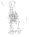
- Figure 4 illustrates a display system, generally 5', incorporating a display controller 10' according to a preferred embodiment of the present invention.
- the display controller 10' is coupled to a frame buffer 20 and a display 40.
- the display controller 10' is preferably coupled to the core 30 by way of a data path 35'.
- the display controller 10' receives and transmits display data over the buses 17, 27 and sends control and synchronisation signals over the paths 15, 25 in a similar fashion to that described with reference to figure 1 above.
- the display controller 10' is also operable to reduce the average amount of power consumed in driving the display by introducing preferably an inter-frame delay period during which no signals are provided to the display 40.
- the supply of display data is preferably interrupted during an inter-frame period in order to minimise any visual effects
- the interruption could occur at any other convenient time such as, for example, during the transmission of lines comprising the so-called 'blanking period' of a frame of video data (the period when non-display data such as teletext or the like is transmitted) or during assertion of the horizontal synchronisation signal.
- the display controller 10' comprises a direct memory access (DMA) controller 50' operable to access display data from the frame buffer 20.
- the display controller 10' also comprises a timing generator 60' operable to provide signals to control the DMA controller 50' and to provide timing and synchronisation signals to the display 40 over the path 25.
- the display controller 10' also comprises a register bank 70' which comprises synchronisation registers 75', a prevention register 80' and a refresh register 90'.
- the synchronisation registers 75' store timing and synchronisation information which is used by the timing generator 60' to determine the timing of the display data sent over bus 27, and the generation of the timing and synchronisation signals sent over bus 25.
- the synchronisation registers 75' provide information regarding the construction and duration of the vertical synchronisation signal 100, the horizontal synchronisation signal 110 and their relationship with respect to the data valid 120 and display data signals 130, 140, 150, 155.
- Clock signal 160 is provided which provides timing information to the frame buffer 20, the display controller 10 and the display 40.
- the timing generator 60' utilises the clock signal when generating, for example, the vertical synchronisation signals 100, horizontal synchronisation signals 110 and data valid signals 120.
- the prevention register 80' stores an indication of the duration of the period of time 'p' for which the generation of the timing and synchronisation signals are prevented from being generated. Whilst preventing the generation of the timing and synchronisation signals, no display data is retrieved from the frame buffer 20, no display data is supplied to the display 40 and the display 40 is not updated.
- the indication stored in this register may be set by the core 30 to suit a particular display based, for example, on the persistence of pixels of the display as derivable from the minimum refresh rate (Rmin) recommended for the display 40. It will be appreciated that the persistence time of the pixels can be estimated to be 1/Rmin. Additionally, or alternatively, the indication stored in the register may be set or varied dynamically based on the characteristics of the display data to be displayed, for example, based on the rate of change of data stored in the frame buffer 20.
- the refresh register 90' stores an indication of whether data stored in the frame buffer 20 differs to that currently being displayed on the display 40. This determination is generally made by the core 30 which will set the refresh register 90' when the data stored in the frame buffer 20 differs to that being displayed on the display 40. As will be explained in more detail below, the timing generator 60' will also refer to the refresh register 90' in order to determine whether, during the predetermined period, to resume the generation of the timing signals in order to update the display 40.
- the core 30 stores a frame of display data in the frame buffer 20 over the data bus 35 for subsequent display on the display 40.
- the display data stored in the frame buffer 20 is periodically updated by the core 30.
- the display controller 10' operates to access the display data stored in the frame buffer 20 and to provide that display data including any necessary timing and synchronisation signals to the display 40 for its display thereon.
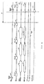
- the DMA controller 50' In order to display a frame of data on the display 40 the DMA controller 50', in response to a signal received from the timing generator 60', sends a data request signal to the frame buffer 20 over the control path 15. Typically, display data corresponding to the first line of the frame is provided to the DMA controller 50' over the data bus 17. Concurrently with the request for display data the timing generator 60' generates the vertical synchronisation signal 100, the characteristics of which are determined by reference to particular values programmed by the core 30 into the synchronisation registers 75', which is transmitted over the timing and synchronisation bus 25.
- the timing generator 60' provides a horizontal synchronisation signal 110 over the timing and synchronisation bus 25 to the display 40.
- the horizontal synchronisation signal 110 is again constructed with reference to particular values stored in the synchronisation registers 75' programmed by the core 30.
- the timing of these synchronisation signals are arranged to conform, for compatibility reasons, to those used by conventional cathode ray tube displays which have been developed to display primarily moving images and whose pixels have a relatively short visual persistence time. It will be appreciated that the duration of the horizontal synchronisation signal 110 will be significantly shorter than that of the vertical synchronisation signal 100.
- the receipt of the vertical synchronisation signal 100 by the display 40 will indicate to the display 40 a beginning of a frame of display data. Thereafter, the receipt of horizontal synchronisation signals 110 indicates to the display 40 the beginning of sequential lines of display data which together form the frame.
- the DMA controller 50' provides the first line of frame data to the display 40 over the data bus 27.
- the timing generator 60' provides a data valid signal 120 over the timing and synchronisation bus 25 to the display 40 to indicate that the first line of display data 130 is now available.
- the display 40 then reads the first line of display data 130 which is then scanned onto the appropriate line of the display 40. Thereafter, this process is repeated for each line of data forming the frame.
- the timing generator 60' transmits a further horizontal synchronisation signal 110 to the display 40 over the timing and synchronisation bus 25 to indicate the end of the last line and that the frame of display data is now complete.
- the display controller 10' provides each frame of display data to the display 40 in a conventional manner, using appropriate timing and control signals for that display. Accordingly, it will be appreciated that the supply of display data to the display 40 remains unchanged.
- the time taken between the first issue of the vertical synchronisation signal 100 indicating the beginning of the frame and the issue of the last horizontal synchronisation signal 110 indicative of the end of the frame will take between 12.5 and 20 milliseconds (i.e. a refresh rate of 50 to 80Hz).
- the timing generator 60' suspends the generation of any further timing, synchronisation or control signals for a predetermined period.
- the timing generator 60' determines the period for which the generation of these signals is suspended by examining the contents of the prevention register 80'.
- the contents of the prevention register 80' are typically programmed by the core 30.
- the value stored in the prevention register 80' is typically selected based on the type of display being used. In order to minimise any undesirable visual effects, such as screen flicker, the value is selected to be less than or equal to the visual persistence time of the pixels forming the display, which can be determined from the recommended minimum refresh rate, Rmin, specified for the display.
- the pixel persistence or visual persistence time is typically in the order of 100 milliseconds. Accordingly, the time between updates of frames of display data can be as long as this persistence time. It will be appreciated that this extended persistence time is due to the provision of a storage element (typically a transistor) for each pixel.
- the value stored in the prevention register 80' may be indicative of up to the persistence time less the time taken to scan a frame of data onto the display. Accordingly, in the example thin film transistor liquid crystal display, the prevention register 80' can store a value representing up to around 80 to 84 milliseconds (100 milliseconds persistence time less 16 to 20 milliseconds scan time).
- the data is supplied and scanned every 100 milliseconds. It will be appreciated that by updating the display 40 in this manner significantly reduces the power consumption of the display system 5'. Also, because the display is rescanned within the persistence time, any undesirable visual effects of the inter-frame delay are minimised.
- timing, control and synchronisation signals Whilst in this preferred embodiment the generation of the timing, control and synchronisation signals is prevented during an inter-frame period, it will be appreciated that the generation of these signals could be prevented at any other time during the frame such as, for example, during the supply of lines of display data (although this may have an undesirable visual effect) or in particular during the supply of display data which corresponds to lines associated with the blanking interval of the frame.
- the generation of timing, synchronisation and control signals and the transmission of display data recommences after the period 'p' indicated by the prevention register 80'.
- a prevention register 80' is shown, it will be appreciated that alternatively the core 30 could instead provide a signal to the timing generator 60' over the data path 35' indicative of the period for which the generation of the timing, synchronisation and control signals is suspended. However, providing such a register reduces the amount of data that needs to be transmitted by the core 30 to the display controller 10'.
- the value stored in the prevention register 80' may be dynamically varied by the core 30 dependent on a number of factors. Such factors include the characteristics of the display data itself (such as whether the frame represents static or moving images), characteristics of the display 40 or, in situations where the display controller 10' drives more than one type of display, then the value can be altered depending on which display is being controlled.
- Figure 6 illustrates an early refresh operation which utilises the refresh register 90' according to a preferred embodiment.
- This optional feature is utilised in order to prevent any unacceptable update latency which may result from the introduction of the inter-frame delay.
- This update latency may occur when the data stored in the frame buffer 20 is changed faster than the rate at which the display 40 is supplied with that data. Such latency can cause a seemingly poor response from the display following, for example, a user action which causes the display data in the frame buffer 20 to be changed, but that change is not rapidly shown on the display 40.
- a signal 170 is provided to the display controller 10' over the data path 35'.
- the refresh register 90' is set.
- the timing generator 60' is responsive to the refresh register 90' it being set. In the event that the refresh register 90' has been set the timing generator 60' then resumes the generation of timing, synchronisation and control signals and lines of display data are retrieved and provided to the display 40 at the appropriate time. Once the display 40 has been updated, the refresh register 90' is then once again cleared.
- TFT LCD thin film transistor
Landscapes
- Engineering & Computer Science (AREA)
- Theoretical Computer Science (AREA)
- Physics & Mathematics (AREA)
- General Physics & Mathematics (AREA)
- Human Computer Interaction (AREA)
- General Engineering & Computer Science (AREA)
- Chemical & Material Sciences (AREA)
- Crystallography & Structural Chemistry (AREA)
- Computer Hardware Design (AREA)
- Control Of Indicators Other Than Cathode Ray Tubes (AREA)
Priority Applications (1)
| Application Number | Priority Date | Filing Date | Title |
|---|---|---|---|
| EP03253549A EP1484737A1 (fr) | 2003-06-05 | 2003-06-05 | Dispositif d'affichage |
Applications Claiming Priority (1)
| Application Number | Priority Date | Filing Date | Title |
|---|---|---|---|
| EP03253549A EP1484737A1 (fr) | 2003-06-05 | 2003-06-05 | Dispositif d'affichage |
Publications (1)
| Publication Number | Publication Date |
|---|---|
| EP1484737A1 true EP1484737A1 (fr) | 2004-12-08 |
Family
ID=33155264
Family Applications (1)
| Application Number | Title | Priority Date | Filing Date |
|---|---|---|---|
| EP03253549A Withdrawn EP1484737A1 (fr) | 2003-06-05 | 2003-06-05 | Dispositif d'affichage |
Country Status (1)
| Country | Link |
|---|---|
| EP (1) | EP1484737A1 (fr) |
Cited By (10)
| Publication number | Priority date | Publication date | Assignee | Title |
|---|---|---|---|---|
| US8988443B2 (en) | 2009-09-25 | 2015-03-24 | Arm Limited | Methods of and apparatus for controlling the reading of arrays of data from memory |
| US9182934B2 (en) | 2013-09-20 | 2015-11-10 | Arm Limited | Method and apparatus for generating an output surface from one or more input surfaces in data processing systems |
| US9195426B2 (en) | 2013-09-20 | 2015-11-24 | Arm Limited | Method and apparatus for generating an output surface from one or more input surfaces in data processing systems |
| US9349156B2 (en) | 2009-09-25 | 2016-05-24 | Arm Limited | Adaptive frame buffer compression |
| US9406155B2 (en) | 2009-09-25 | 2016-08-02 | Arm Limited | Graphics processing systems |
| US9640131B2 (en) | 2014-02-07 | 2017-05-02 | Arm Limited | Method and apparatus for overdriving based on regions of a frame |
| US9881401B2 (en) | 2009-09-25 | 2018-01-30 | Arm Limited | Graphics processing system |
| US9996363B2 (en) | 2011-04-04 | 2018-06-12 | Arm Limited | Methods of and apparatus for displaying windows on a display |
| US10194156B2 (en) | 2014-07-15 | 2019-01-29 | Arm Limited | Method of and apparatus for generating an output frame |
| US10832639B2 (en) | 2015-07-21 | 2020-11-10 | Arm Limited | Method of and apparatus for generating a signature representative of the content of an array of data |
Citations (4)
| Publication number | Priority date | Publication date | Assignee | Title |
|---|---|---|---|---|
| US5181131A (en) * | 1988-11-11 | 1993-01-19 | Semiconductor Energy Laboratory Co., Ltd. | Power conserving driver circuit for liquid crystal displays |
| US5686934A (en) * | 1991-08-02 | 1997-11-11 | Canon Kabushiki Kaisha | Display control apparatus |
| EP1035536A2 (fr) * | 1999-03-12 | 2000-09-13 | Minolta Co., Ltd. | Dispositif électronique portable à affichage à cristaux liquides et sa méthode de commande |
| US20020036616A1 (en) * | 2000-05-26 | 2002-03-28 | Satoshi Inoue | Display device and recording medium |
-
2003
- 2003-06-05 EP EP03253549A patent/EP1484737A1/fr not_active Withdrawn
Patent Citations (4)
| Publication number | Priority date | Publication date | Assignee | Title |
|---|---|---|---|---|
| US5181131A (en) * | 1988-11-11 | 1993-01-19 | Semiconductor Energy Laboratory Co., Ltd. | Power conserving driver circuit for liquid crystal displays |
| US5686934A (en) * | 1991-08-02 | 1997-11-11 | Canon Kabushiki Kaisha | Display control apparatus |
| EP1035536A2 (fr) * | 1999-03-12 | 2000-09-13 | Minolta Co., Ltd. | Dispositif électronique portable à affichage à cristaux liquides et sa méthode de commande |
| US20020036616A1 (en) * | 2000-05-26 | 2002-03-28 | Satoshi Inoue | Display device and recording medium |
Non-Patent Citations (2)
| Title |
|---|
| CARTS-POWELL Y: "CHOLESTERIC LCDS SHOW IMAGES AFTER POWER IS TURNED OFF", LASER FOCUS WORLD, PENNWELL PUBLISHING, TULSA, US, vol. 34, no. 9, September 1998 (1998-09-01), pages 99 - 101,103, XP001031931, ISSN: 1043-8092 * |
| MACLEOD A: "FERROELECTRIC DISPLAY DOES NOT NEED REFRESH", NEW ELECTRONICS, INTERNATIONAL THOMSON PUBLISHING, LONDON, GB, vol. 24, no. 11, 1 December 1991 (1991-12-01), pages 28 - 29,31, XP000310176, ISSN: 0047-9624 * |
Cited By (10)
| Publication number | Priority date | Publication date | Assignee | Title |
|---|---|---|---|---|
| US8988443B2 (en) | 2009-09-25 | 2015-03-24 | Arm Limited | Methods of and apparatus for controlling the reading of arrays of data from memory |
| US9349156B2 (en) | 2009-09-25 | 2016-05-24 | Arm Limited | Adaptive frame buffer compression |
| US9406155B2 (en) | 2009-09-25 | 2016-08-02 | Arm Limited | Graphics processing systems |
| US9881401B2 (en) | 2009-09-25 | 2018-01-30 | Arm Limited | Graphics processing system |
| US9996363B2 (en) | 2011-04-04 | 2018-06-12 | Arm Limited | Methods of and apparatus for displaying windows on a display |
| US9182934B2 (en) | 2013-09-20 | 2015-11-10 | Arm Limited | Method and apparatus for generating an output surface from one or more input surfaces in data processing systems |
| US9195426B2 (en) | 2013-09-20 | 2015-11-24 | Arm Limited | Method and apparatus for generating an output surface from one or more input surfaces in data processing systems |
| US9640131B2 (en) | 2014-02-07 | 2017-05-02 | Arm Limited | Method and apparatus for overdriving based on regions of a frame |
| US10194156B2 (en) | 2014-07-15 | 2019-01-29 | Arm Limited | Method of and apparatus for generating an output frame |
| US10832639B2 (en) | 2015-07-21 | 2020-11-10 | Arm Limited | Method of and apparatus for generating a signature representative of the content of an array of data |
Similar Documents
| Publication | Publication Date | Title |
|---|---|---|
| KR101025343B1 (ko) | 스테레오 글래스 셔터를 제어하는 시스템, 방법, 및 컴퓨터 판독 가능 기록 매체 | |
| US8643658B2 (en) | Techniques for aligning frame data | |
| EP2293272B1 (fr) | Réglage de fréquences d'images dynamique | |
| CN1981519B (zh) | 用于显示图像帧序列的方法和系统 | |
| JP6703800B2 (ja) | 表示装置、表示装置の制御方法、および制御プログラム | |
| US8823721B2 (en) | Techniques for aligning frame data | |
| US20140009480A1 (en) | Display system with display panel and display controller and driver having moving picture interface | |
| US8207974B2 (en) | Switch for graphics processing units | |
| EP1999740A2 (fr) | Systeme, procede et produit-programme informatique pour commander des obturateurs de lunettes stereo | |
| JP5058434B2 (ja) | Lcd動作電流を減少させるタイミングコントローラとlcdドライバとディスプレイデータ出力方法 | |
| JP2002123223A (ja) | 液晶表示装置及びコンピュータ | |
| US6844879B2 (en) | Drawing apparatus | |
| JP2011043827A (ja) | 画像表示装置、画像表示モニター、およびテレビジョン受像機 | |
| JP6609313B2 (ja) | 制御装置、表示装置、制御方法、および制御プログラム | |
| EP1484737A1 (fr) | Dispositif d'affichage | |
| US8867115B2 (en) | Control of array of two-dimensional imaging elements in light modulating displays | |
| US8194065B1 (en) | Hardware system and method for changing a display refresh rate | |
| US9087473B1 (en) | System, method, and computer program product for changing a display refresh rate in an active period | |
| US10896660B2 (en) | Display control device, display device, and display control method | |
| US11854476B1 (en) | Timing controller having mechanism for frame synchronization, display panel thereof, and display system thereof | |
| CN114153416B (zh) | 一种显示控制的方法及相关装置 | |
| US20230419892A1 (en) | Display driving method and apparatus, display driver integrated circuit chip and terminal | |
| US7046227B2 (en) | System and method for continuously tracing transfer rectangles for image data transfers | |
| JP2002221944A (ja) | 液晶表示パネルの駆動装置、情報端末装置、液晶表示の制御方法、およびプログラム | |
| US20060012602A1 (en) | System and method for efficiently performing automatic partial transfers of image data |
Legal Events
| Date | Code | Title | Description |
|---|---|---|---|
| PUAI | Public reference made under article 153(3) epc to a published international application that has entered the european phase |
Free format text: ORIGINAL CODE: 0009012 |
|
| AK | Designated contracting states |
Kind code of ref document: A1 Designated state(s): AT BE BG CH CY CZ DE DK EE ES FI FR GB GR HU IE IT LI LU MC NL PT RO SE SI SK TR |
|
| AX | Request for extension of the european patent |
Extension state: AL LT LV MK |
|
| AKX | Designation fees paid | ||
| REG | Reference to a national code |
Ref country code: DE Ref legal event code: 8566 |
|
| STAA | Information on the status of an ep patent application or granted ep patent |
Free format text: STATUS: THE APPLICATION IS DEEMED TO BE WITHDRAWN |
|
| 18D | Application deemed to be withdrawn |
Effective date: 20050609 |