EP1483722B1 - Speichermodulbaugruppe, die teilweise defekte chips verwendet - Google Patents
Speichermodulbaugruppe, die teilweise defekte chips verwendet Download PDFInfo
- Publication number
- EP1483722B1 EP1483722B1 EP03713706A EP03713706A EP1483722B1 EP 1483722 B1 EP1483722 B1 EP 1483722B1 EP 03713706 A EP03713706 A EP 03713706A EP 03713706 A EP03713706 A EP 03713706A EP 1483722 B1 EP1483722 B1 EP 1483722B1
- Authority
- EP
- European Patent Office
- Prior art keywords
- clock
- memory
- memory parts
- patching
- parts
- Prior art date
- Legal status (The legal status is an assumption and is not a legal conclusion. Google has not performed a legal analysis and makes no representation as to the accuracy of the status listed.)
- Expired - Lifetime
Links
Images





Classifications
-
- G—PHYSICS
- G11—INFORMATION STORAGE
- G11C—STATIC STORES
- G11C7/00—Arrangements for writing information into, or reading information out from, a digital store
-
- H—ELECTRICITY
- H10—SEMICONDUCTOR DEVICES; ELECTRIC SOLID-STATE DEVICES NOT OTHERWISE PROVIDED FOR
- H10P—GENERIC PROCESSES OR APPARATUS FOR THE MANUFACTURE OR TREATMENT OF DEVICES COVERED BY CLASS H10
- H10P74/00—Testing or measuring during manufacture or treatment of wafers, substrates or devices
- H10P74/23—Testing or measuring during manufacture or treatment of wafers, substrates or devices characterised by multiple measurements, corrections, marking or sorting processes
-
- B—PERFORMING OPERATIONS; TRANSPORTING
- B82—NANOTECHNOLOGY
- B82Y—SPECIFIC USES OR APPLICATIONS OF NANOSTRUCTURES; MEASUREMENT OR ANALYSIS OF NANOSTRUCTURES; MANUFACTURE OR TREATMENT OF NANOSTRUCTURES
- B82Y10/00—Nanotechnology for information processing, storage or transmission, e.g. quantum computing or single electron logic
-
- G—PHYSICS
- G11—INFORMATION STORAGE
- G11C—STATIC STORES
- G11C11/00—Digital stores characterised by the use of particular electric or magnetic storage elements; Storage elements therefor
- G11C11/21—Digital stores characterised by the use of particular electric or magnetic storage elements; Storage elements therefor using electric elements
- G11C11/34—Digital stores characterised by the use of particular electric or magnetic storage elements; Storage elements therefor using electric elements using semiconductor devices
- G11C11/40—Digital stores characterised by the use of particular electric or magnetic storage elements; Storage elements therefor using electric elements using semiconductor devices using transistors
-
- G—PHYSICS
- G11—INFORMATION STORAGE
- G11C—STATIC STORES
- G11C29/00—Checking stores for correct operation ; Subsequent repair; Testing stores during standby or offline operation
-
- G—PHYSICS
- G11—INFORMATION STORAGE
- G11C—STATIC STORES
- G11C29/00—Checking stores for correct operation ; Subsequent repair; Testing stores during standby or offline operation
- G11C29/02—Detection or location of defective auxiliary circuits, e.g. defective refresh counters
- G11C29/022—Detection or location of defective auxiliary circuits, e.g. defective refresh counters in I/O circuitry
-
- G—PHYSICS
- G11—INFORMATION STORAGE
- G11C—STATIC STORES
- G11C29/00—Checking stores for correct operation ; Subsequent repair; Testing stores during standby or offline operation
- G11C29/70—Masking faults in memories by using spares or by reconfiguring
- G11C29/88—Masking faults in memories by using spares or by reconfiguring with partially good memories
-
- G—PHYSICS
- G11—INFORMATION STORAGE
- G11C—STATIC STORES
- G11C29/00—Checking stores for correct operation ; Subsequent repair; Testing stores during standby or offline operation
- G11C29/70—Masking faults in memories by using spares or by reconfiguring
- G11C29/88—Masking faults in memories by using spares or by reconfiguring with partially good memories
- G11C29/886—Masking faults in memories by using spares or by reconfiguring with partially good memories combining plural defective memory devices to provide a contiguous address range, e.g. one device supplies working blocks to replace defective blocks in another device
-
- G—PHYSICS
- G11—INFORMATION STORAGE
- G11C—STATIC STORES
- G11C5/00—Details of stores covered by group G11C11/00
- G11C5/06—Arrangements for interconnecting storage elements electrically, e.g. by wiring
- G11C5/063—Voltage and signal distribution in integrated semi-conductor memory access lines, e.g. word-line, bit-line, cross-over resistance, propagation delay
-
- H—ELECTRICITY
- H05—ELECTRIC TECHNIQUES NOT OTHERWISE PROVIDED FOR
- H05K—PRINTED CIRCUITS; CASINGS OR CONSTRUCTIONAL DETAILS OF ELECTRIC APPARATUS; MANUFACTURE OF ASSEMBLAGES OF ELECTRICAL COMPONENTS
- H05K1/00—Printed circuits
- H05K1/02—Details
- H05K1/0286—Programmable, customizable or modifiable circuits
- H05K1/029—Programmable, customizable or modifiable circuits having a programmable lay-out, i.e. adapted for choosing between a few possibilities
-
- H—ELECTRICITY
- H05—ELECTRIC TECHNIQUES NOT OTHERWISE PROVIDED FOR
- H05K—PRINTED CIRCUITS; CASINGS OR CONSTRUCTIONAL DETAILS OF ELECTRIC APPARATUS; MANUFACTURE OF ASSEMBLAGES OF ELECTRICAL COMPONENTS
- H05K1/00—Printed circuits
- H05K1/02—Details
- H05K1/0286—Programmable, customizable or modifiable circuits
- H05K1/0292—Programmable, customizable or modifiable circuits having a modifiable lay-out, i.e. adapted for engineering changes or repair
-
- H—ELECTRICITY
- H10—SEMICONDUCTOR DEVICES; ELECTRIC SOLID-STATE DEVICES NOT OTHERWISE PROVIDED FOR
- H10W—GENERIC PACKAGES, INTERCONNECTIONS, CONNECTORS OR OTHER CONSTRUCTIONAL DETAILS OF DEVICES COVERED BY CLASS H10
- H10W42/00—Arrangements for protection of devices
- H10W42/121—Arrangements for protection of devices protecting against mechanical damage
-
- H—ELECTRICITY
- H05—ELECTRIC TECHNIQUES NOT OTHERWISE PROVIDED FOR
- H05K—PRINTED CIRCUITS; CASINGS OR CONSTRUCTIONAL DETAILS OF ELECTRIC APPARATUS; MANUFACTURE OF ASSEMBLAGES OF ELECTRICAL COMPONENTS
- H05K1/00—Printed circuits
- H05K1/18—Printed circuits structurally associated with non-printed electric components
- H05K1/181—Printed circuits structurally associated with non-printed electric components associated with surface mounted components
-
- H—ELECTRICITY
- H05—ELECTRIC TECHNIQUES NOT OTHERWISE PROVIDED FOR
- H05K—PRINTED CIRCUITS; CASINGS OR CONSTRUCTIONAL DETAILS OF ELECTRIC APPARATUS; MANUFACTURE OF ASSEMBLAGES OF ELECTRICAL COMPONENTS
- H05K2201/00—Indexing scheme relating to printed circuits covered by H05K1/00
- H05K2201/10—Details of components or other objects attached to or integrated in a printed circuit board
- H05K2201/10007—Types of components
- H05K2201/10159—Memory
-
- H—ELECTRICITY
- H05—ELECTRIC TECHNIQUES NOT OTHERWISE PROVIDED FOR
- H05K—PRINTED CIRCUITS; CASINGS OR CONSTRUCTIONAL DETAILS OF ELECTRIC APPARATUS; MANUFACTURE OF ASSEMBLAGES OF ELECTRICAL COMPONENTS
- H05K2203/00—Indexing scheme relating to apparatus or processes for manufacturing printed circuits covered by H05K3/00
- H05K2203/16—Inspection; Monitoring; Aligning
- H05K2203/162—Testing a finished product, e.g. heat cycle testing of solder joints
-
- H—ELECTRICITY
- H10—SEMICONDUCTOR DEVICES; ELECTRIC SOLID-STATE DEVICES NOT OTHERWISE PROVIDED FOR
- H10W—GENERIC PACKAGES, INTERCONNECTIONS, CONNECTORS OR OTHER CONSTRUCTIONAL DETAILS OF DEVICES COVERED BY CLASS H10
- H10W72/00—Interconnections or connectors in packages
- H10W72/50—Bond wires
- H10W72/581—Auxiliary members, e.g. flow barriers
Definitions
- the present invention relates to the field of electronic memory modules. More specifically, embodiments of the present invention relate to the fabrication of DDR memory and other logic modules that selectively use operating segments of a plurality of less-than-perfect chips or packages exclusively, or in combination with perfect ones.
- DDR Double Data Rate
- a method and apparatus disclosed herein for manufacturing DDR and other memory modules uses partially-defective memory parts or a combination of partially-defective and flawless memory parts.
- the method and apparatus include an improved clocking method and system, which enables an indeterminate number of memory parts to be used without distorting the clock signal.
- a Phase-Lock Loop circuit is used to significantly reduce clock distortion on DDR and other memory modules.
- Fig. 1 is a flowchart illustrating a method of fabricating a memory module according to one embodiment.
- a clock booster is mounted on a multi-layer circuit board (101).
- the clock booster may be any apparatus that receives a clock input, and outputs one or more clock signals capable of driving a multiplicity of logic parts without clock distortion.
- a Phase-Locked Loop circuit may be used as a clock booster.
- memory parts are tested and patched (102).
- the testing and patching (102) allows a fully-functional memory module to be fabricated using partially-defective parts. Due to the load that each memory part adds, it is desirable to only connect the clock signal to those memory parts that are utilized. This may be accomplished using any number of switching mechanisms to connect or disconnect a clock signal to a memory part.
- a clock patching network may be used to selectively connect or disconnect outputs of a clock booster to the memory parts (103).
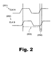
- Fig. 2 is a graph illustrating a distortion of a clock signal due to clock skew.
- clock skew may be described as a decrease of available time in a clock cycle.
- CLK A (201) produces a clock signal with a fixed frequency
- CLK B (202) slightly trails the signal for CLK A (201). Because the two clocks are not synchronized there is a loss (204) in the clock period. For example, if two memory parts were being accessed at the same time, one with CLK A and the other with CLK B, the effective clock period (203) would be reduced because the clock signals are not synchronized. For many memory modules it may be desirable to access up to 16 memory parts at the same time.
- clock skew an important design issue since clock skew is often caused by variations in the load the clock is driving, etc.
- applications such as DDR that use both the rising and falling edge of a clock are sensitive to reductions in clock period caused by clock skew.
- Fig. 3 is a graph illustrating a distortion of a clock signal due to electrical noise. Electrical noise is common in high frequency electrical applications, and is detrimental in memory units. As shown in Fig. 3, a clock signal (301) is rising from a logic low level (302) to a logic high level (303).
- a logic threshold level (304) to distinguish when a clock signal (301) is "high” or “low.” For example, when the clock signal (301) reaches point 1 (305), a device using the clock signal will recognize a logic high (303), but a period of electrical noise (306) on the clock signal may cause the clock (301) signal to dip below the logic threshold value (304), resulting in extraneous clocking when the clock signal (301) again crosses the logic threshold value (304) at point 2 (307). A period of electrical noise (306) on a clock signal (301) may consequently cause double clocking, false clocking, and waveform distortion, etc.
- a device that strengthens a clock signal to allow a high number of memory parts to be driven by that clock signal is desirable.
- Fig. 4 illustrates a schematic diagram of a Phase-Locked Loop circuit that may be used as a clock booster for a memory module according to one embodiment of the present invention.
- a PPL unit (407) may comprise a number of buffer units (417), PPL circuitry (406), and a mux (409).
- Several signals including a clock signal, CLK (401), Inv_CLK (402), FBin (403), Inv_FBin (404), VCC (408), and Output Enable (423) are supplied as input signals to the PPL unit (407).
- Fig. 5 is a block diagram illustrating a layout of major components of a memory module fabricated according to one selected embodiment.
- a 64M(megabytes), 128M, or 256M DDR or SDR memory module fabricated using 8Mx8, 16Mx8, or 32Mx8 memory parts may be illustrated by the memory module of Fig. 5.
- the memory module (500) may comprise a multi-layer circuit board (531), paired memory parts (532), patching networks (533), and a selectively operable clock booster (507), such as the PPL unit (407, Fig. 4) shown in Fig. 4.
- the paired memory parts (532) are designated by P1, P2, P3, and P4, with each pair preferably comprising one primary and one secondary memory part.
- Fig. 6 is a block diagram illustrating a primary and secondary memory part in conjunction with a patching network.
- the I/O lines (I/O 1-I/O 8) of a primary memory part (601) may be connected to pads (604) of a patching network (603).
- each pad (604) to which a separate primary I/O line is connected is preferably close to a separate output line (Out1-Out8).
- the backup I/O lines (I/O 1b-I/O 8b) from a secondary memory part (602) are also connected to pads (604) of the patching network (603).
- the patching network (703) is used to connect a primary or secondary I/O line to an output line (Out1-Out2). This may be accomplished by connecting a single pad (704) corresponding to a primary I/O line or backup I/O line to one of six pads (704) corresponding to each output line. Electrically conductive materials, e.g., solder, jumper wires, etc., may be used to connect pads (704) of the patching network (703) to allow a host device to access the I/O bits of a primary memory part (701) or secondary memory part (702).
- Fig. 8 is a block diagram illustrating a primary and secondary memory part in conjunction with another patching network.
- two I/O lines (I/O 1-I/O 2) of a primary memory part (801) may be connected to two separate pads (804) of a patching network (803).
- eight backup I/O lines (I/O 1b-I/O 8b) are connected to eight other pads (804) of the patching network (803).
- each output line (Out1-Out2) is connected to a series of pads (804), thus providing a separate connective pad (804) adjacent to each pad (804) corresponding to an I/O line.
- Fig. 7 illustrates two primary I/O lines and eight backup I/O lines connected to ten separate pads (804) of the patching network (803). Therefore, each output line is connected to ten pads (804) adjacent to the pads (804) corresponding to the primary and secondary I/O lines.
- FIG. 8 The illustration of FIG. 8 is incomplete in that only one patching network (803) is shown.
- additional patching networks (803) are preferred, wherein two primary I/O lines and all eight backup I/O lines are connected to each patching network (803). Therefore, a memory module using the patching configuration shown in FIG. 8, would preferably use four patching networks (803) for each primary memory part (801) and secondary memory part (802) pair.
- the spacing between the pads (804) shown in FIG. 8 is for illustrative purposes only. In a real implementation, pads (804) are preferably close together, thus allowing electrical connections between pads (804) corresponding to I/O lines and pads (804) corresponding to output lines to be easily made.
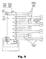
- FIG. 9 is a block diagram illustrating a PLL clock driver, which may be selectively connected to a number of memory parts in one selected embodiment.
- a PPL unit (907) e.g., the PPL unit (407, FIG. 4) described in FIG. 4, receives a clock signal, CLK (901), from which a number of outputs (synthesized copies of the incoming clock signal) are created. These outputs are connected to primary memory parts (932) and secondary memory parts (933) through switches (924).
- the switches (924) may selectively be opened or closed, thereby allowing a clock signal to be used preferably only with memory parts (932, 933) whose I/O lines are accessed.
- the PPL unit (907) may be enabled or disabled using an enable switch (926).
- FIG. 10 is similar to FIG. 9 in that FIG. 10 is a block diagram illustrating a PLL clock driver, which may be selectively connected to a number of memory parts.
- a PPL unit (1007) e.g., the PPL unit (407, FIG. 4) described in FIG. 4, receives a clock signal, CLK (1001), from which a number of outputs (synthesized copies of the incoming clock signal) are created.
- CLK clock signal
- These outputs may preferably be connected to primary memory parts (1032) and secondary memory parts (1033) through a clock patching network (1025), which uses pads (1024) to selectively complete a connection, thereby allowing a clock signal to be used preferably only with memory parts (1032, 1033) whose I/O lines are accessed.
- the PPL unit (1007) may be enabled or disabled using an enable switch (1026).
- FIG. 11 is a block diagram illustrating a PLL clock driver, selectively connected to a number of memory parts.
- a PPL unit (1107) e.g., the PPL unit (407, FIG. 4) described in FIG. 4, receives a clock signal, CLK (1101), from which a number of outputs (synthesized copies of the incoming clock signal) are created. These outputs may preferably be connected to primary memory parts (1132) and secondary memory parts (1133) through a clock patching network (1125), which uses pads (1124) to selectively complete a connection, thereby allowing a clock signal to be used preferably only with memory parts (1132, 1133) whose I/O lines are accessed. Additionally, the PPL unit (1107) may be enabled or disabled using an enable switch (1126).
- solder dots (1127) or jumper wires (1128) may be used.
- a protective material (1129) e.g., a thermally curable material, may be used to physically protect jumper wires (1128), solder dots (1127), etc.
- all of the memory parts (1132, 1133) are connected to a clock output from the PPL (1107) with exception of the secondary memory part (1133) associated with the memory part pair, P2.
- this illustration is preferable if I/O lines of all memory parts are utilized to create a fully-functional memory module except the secondary memory part of P2.
Landscapes
- Engineering & Computer Science (AREA)
- Microelectronics & Electronic Packaging (AREA)
- Chemical & Material Sciences (AREA)
- Nanotechnology (AREA)
- Theoretical Computer Science (AREA)
- Crystallography & Structural Chemistry (AREA)
- Physics & Mathematics (AREA)
- Mathematical Physics (AREA)
- Computer Hardware Design (AREA)
- Techniques For Improving Reliability Of Storages (AREA)
- Semiconductor Memories (AREA)
- For Increasing The Reliability Of Semiconductor Memories (AREA)
- Semiconductor Integrated Circuits (AREA)
- Dram (AREA)
Claims (9)
- Verfahren zum selektiven Implementieren eines Taktverstärkers (Clock Booster), wobei das Verfahren die folgenden Schritte umfasst:Montieren eines Taktverstärkers (507) auf einer mehrlagigen Leiterplatte (101);Testen und Patchen von Speicherteilen, einschließlich teilweise defekter Speicherteile, um ein voll funktionsfähiges Speichermodul (102) zu erzielen; und je nach dem Testergebnis, selektives Verbinden des genannten Taktverstärkers mit den genannten gepatchten Speicherteilen, deren E/A-Leitungen verwendet werden (103).
- Verfahren nach Anspruch 1, bei dem der genannte Taktverstärker (507) eine Phasenregelkreisschaltung (407) umfasst.
- Verfahren nach Anspruch 1, bei dem das genannte Testen (102) E/A-Leitungsfunktionstests umfasst.
- Verfahren Anspruch 1, bei das genannte selektive Verbinden eines Taktverstärkers (507) die Verwendung eines Taktpatching-Netzwerks (603) zum Verbinden eines Taktsignals mit den genannten Speicherteilen (601) umfasst.
- Verfahren nach Anspruch 4, bei dem das genannte Taktsignal einen Ausgang von dem genannten Taktverstärker (507) umfasst.
- Speichermodul (500), das mit dem Verfahren nach Anspruch 1 hergestellt wurde.
- Mehrlagige Leiterplatte (531) zum Herstellen eines Speichermoduls mit einem selektiv zu betreibenden Taktverstärker (507) und teilweise defekten Speicherteilen (601), wobei die genannte Leiterplatte Folgendes umfasst:Mittel zum Testen und Patchen von Speicherteilen, einschließlich teilweise defekter Speicherteile, um ein voll funktionelles Speichermodul (102) zu erzielen; undMittel zum selektiven Verbinden des genannten Taktverstärkers mit den genannten gepatchten Speicherteilen, deren E/A-Leitungen benutzt werden (103).
- Mehrlagige Leiterplatte nach Anspruch 7, wobei die genannte Platte ein Mittel zum Verwenden einer unbestimmten Anzahl von Speicherteilen (532) umfasst, das Patching-Netzwerke (533) umfasst.
- Mehrlagige Leiterplatte nach Anspruch 7, wobei das genannte Mittel zum selektiven Verbinden des genannten Taktverstärkers (507) mit den genannten Speicherteilen (532) ein Taktpatching-Netzwerk (533) umfasst.
Priority Applications (1)
| Application Number | Priority Date | Filing Date | Title |
|---|---|---|---|
| EP06115412A EP1699056A1 (de) | 2002-02-26 | 2003-02-24 | Halbleiterspeichermodul und mehrschichtige Leiterplatte zur Herstellung eines Speichermoduls |
Applications Claiming Priority (5)
| Application Number | Priority Date | Filing Date | Title |
|---|---|---|---|
| US36003602P | 2002-02-26 | 2002-02-26 | |
| US360036P | 2002-02-26 | ||
| US10/371,736 US20030161198A1 (en) | 2002-02-26 | 2003-02-20 | Method and apparatus for implementing a selectively operable clock booster for DDR memory or other logic modules which utilize partially-defective memory parts, or a combination of partially-defective and flawless memory parts |
| US371736 | 2003-02-20 | ||
| PCT/US2003/005845 WO2003073356A1 (en) | 2002-02-26 | 2003-02-24 | Memory module assembly using partially defective chips |
Related Child Applications (1)
| Application Number | Title | Priority Date | Filing Date |
|---|---|---|---|
| EP06115412A Division EP1699056A1 (de) | 2002-02-26 | 2003-02-24 | Halbleiterspeichermodul und mehrschichtige Leiterplatte zur Herstellung eines Speichermoduls |
Publications (3)
| Publication Number | Publication Date |
|---|---|
| EP1483722A1 EP1483722A1 (de) | 2004-12-08 |
| EP1483722A4 EP1483722A4 (de) | 2005-04-27 |
| EP1483722B1 true EP1483722B1 (de) | 2007-04-18 |
Family
ID=27760587
Family Applications (2)
| Application Number | Title | Priority Date | Filing Date |
|---|---|---|---|
| EP06115412A Withdrawn EP1699056A1 (de) | 2002-02-26 | 2003-02-24 | Halbleiterspeichermodul und mehrschichtige Leiterplatte zur Herstellung eines Speichermoduls |
| EP03713706A Expired - Lifetime EP1483722B1 (de) | 2002-02-26 | 2003-02-24 | Speichermodulbaugruppe, die teilweise defekte chips verwendet |
Family Applications Before (1)
| Application Number | Title | Priority Date | Filing Date |
|---|---|---|---|
| EP06115412A Withdrawn EP1699056A1 (de) | 2002-02-26 | 2003-02-24 | Halbleiterspeichermodul und mehrschichtige Leiterplatte zur Herstellung eines Speichermoduls |
Country Status (10)
| Country | Link |
|---|---|
| US (1) | US20030161198A1 (de) |
| EP (2) | EP1699056A1 (de) |
| KR (1) | KR20050002834A (de) |
| AT (1) | ATE360252T1 (de) |
| AU (1) | AU2003217745A1 (de) |
| CA (1) | CA2477754A1 (de) |
| DE (1) | DE60313302T2 (de) |
| DK (1) | DK1483722T3 (de) |
| ES (1) | ES2283760T3 (de) |
| WO (1) | WO2003073356A1 (de) |
Family Cites Families (16)
| Publication number | Priority date | Publication date | Assignee | Title |
|---|---|---|---|---|
| JPH0738274B2 (ja) * | 1988-12-22 | 1995-04-26 | 株式会社東芝 | 不揮発性半導体メモリシステム |
| US4922128A (en) * | 1989-01-13 | 1990-05-01 | Ibm Corporation | Boost clock circuit for driving redundant wordlines and sample wordlines |
| US5208178A (en) * | 1990-08-02 | 1993-05-04 | Hitachi, Ltd. | Manufacturing a semiconductor integrated circuit device having on chip logic correction |
| US5655113A (en) * | 1994-07-05 | 1997-08-05 | Monolithic System Technology, Inc. | Resynchronization circuit for a memory system and method of operating same |
| JP3273440B2 (ja) * | 1994-10-19 | 2002-04-08 | マイクロン・テクノロジー・インコーポレーテッド | 部分的に良好なメモリ集積回路から使用可能な部分を得るための効率的な方法 |
| IN188196B (de) * | 1995-05-15 | 2002-08-31 | Silicon Graphics Inc | |
| JPH09282900A (ja) * | 1996-04-11 | 1997-10-31 | Oki Electric Ind Co Ltd | メモリモジュール |
| US6119049A (en) * | 1996-08-12 | 2000-09-12 | Tandon Associates, Inc. | Memory module assembly using partially defective chips |
| US5867448A (en) * | 1997-06-11 | 1999-02-02 | Cypress Semiconductor Corp. | Buffer for memory modules with trace delay compensation |
| US6351827B1 (en) * | 1998-04-08 | 2002-02-26 | Kingston Technology Co. | Voltage and clock margin testing of memory-modules using an adapter board mounted to a PC motherboard |
| US6195762B1 (en) * | 1998-06-24 | 2001-02-27 | Micron Techonology, Inc. | Circuit and method for masking a dormant memory cell |
| US6282210B1 (en) * | 1998-08-12 | 2001-08-28 | Staktek Group L.P. | Clock driver with instantaneously selectable phase and method for use in data communication systems |
| JP4480855B2 (ja) * | 2000-06-08 | 2010-06-16 | 富士通マイクロエレクトロニクス株式会社 | 半導体デバイスを含むモジュール、及びモジュールを含むシステム |
| US6445625B1 (en) * | 2000-08-25 | 2002-09-03 | Micron Technology, Inc. | Memory device redundancy selection having test inputs |
| US6711695B1 (en) * | 2001-01-26 | 2004-03-23 | Hewlett-Packard Development Company, L.P. | PECL voltage DIMM with remote multi-module etch skew compensation |
| US6763444B2 (en) * | 2001-05-08 | 2004-07-13 | Micron Technology, Inc. | Read/write timing calibration of a memory array using a row or a redundant row |
-
2003
- 2003-02-20 US US10/371,736 patent/US20030161198A1/en not_active Abandoned
- 2003-02-24 KR KR10-2004-7013211A patent/KR20050002834A/ko not_active Withdrawn
- 2003-02-24 DE DE60313302T patent/DE60313302T2/de not_active Expired - Fee Related
- 2003-02-24 WO PCT/US2003/005845 patent/WO2003073356A1/en not_active Ceased
- 2003-02-24 CA CA002477754A patent/CA2477754A1/en not_active Abandoned
- 2003-02-24 DK DK03713706T patent/DK1483722T3/da active
- 2003-02-24 EP EP06115412A patent/EP1699056A1/de not_active Withdrawn
- 2003-02-24 AU AU2003217745A patent/AU2003217745A1/en not_active Abandoned
- 2003-02-24 AT AT03713706T patent/ATE360252T1/de not_active IP Right Cessation
- 2003-02-24 EP EP03713706A patent/EP1483722B1/de not_active Expired - Lifetime
- 2003-02-24 ES ES03713706T patent/ES2283760T3/es not_active Expired - Lifetime
Also Published As
| Publication number | Publication date |
|---|---|
| AU2003217745A1 (en) | 2003-09-09 |
| EP1483722A1 (de) | 2004-12-08 |
| CA2477754A1 (en) | 2003-09-04 |
| ATE360252T1 (de) | 2007-05-15 |
| DE60313302D1 (de) | 2007-05-31 |
| DE60313302T2 (de) | 2008-01-03 |
| WO2003073356A8 (en) | 2004-07-29 |
| EP1699056A1 (de) | 2006-09-06 |
| ES2283760T3 (es) | 2007-11-01 |
| US20030161198A1 (en) | 2003-08-28 |
| DK1483722T3 (da) | 2007-06-25 |
| EP1483722A4 (de) | 2005-04-27 |
| WO2003073356A1 (en) | 2003-09-04 |
| AU2003217745A8 (en) | 2003-09-09 |
| KR20050002834A (ko) | 2005-01-10 |
Similar Documents
| Publication | Publication Date | Title |
|---|---|---|
| US11043258B2 (en) | Memory system topologies including a memory die stack | |
| US7729151B2 (en) | System including a buffered memory module | |
| KR101533120B1 (ko) | 멀티 다이 메모리 디바이스 | |
| US11328764B2 (en) | Memory system topologies including a memory die stack | |
| US20030090879A1 (en) | Dual inline memory module | |
| US8928349B2 (en) | On-die termination circuit, semiconductor memory device and memory system | |
| CN102859598A (zh) | 平衡式裸片上终结 | |
| US20070115712A1 (en) | Apparatus and method for mounting microelectronic devices on a mirrored board assembly | |
| US20230401008A1 (en) | Command address input buffer bias current reduction | |
| EP1483722B1 (de) | Speichermodulbaugruppe, die teilweise defekte chips verwendet | |
| US5828608A (en) | Selectively decoupled I/O latch | |
| US11967355B2 (en) | Systems for reducing inconsistencies across current mirror | |
| US6556051B2 (en) | Apparatus for providing both supports including synchronous dynamic random access memory (SDRAM) module and double data rate (DDR) DRAM module | |
| KR20070028064A (ko) | 반도체 메모리 장치 및 그 병렬 테스트 연결을 통한직류특성 테스트 방법 | |
| US7060512B2 (en) | Patching methods and apparatus for fabricating memory modules | |
| CA2477763A1 (en) | Methods and apparatus for fabricating chip-on-board modules |
Legal Events
| Date | Code | Title | Description |
|---|---|---|---|
| PUAI | Public reference made under article 153(3) epc to a published international application that has entered the european phase |
Free format text: ORIGINAL CODE: 0009012 |
|
| 17P | Request for examination filed |
Effective date: 20040830 |
|
| AK | Designated contracting states |
Kind code of ref document: A1 Designated state(s): AT BE BG CH CY CZ DE DK EE ES FI FR GB GR HU IE IT LI LU MC NL PT SE SI SK TR |
|
| AX | Request for extension of the european patent |
Extension state: AL LT LV MK RO |
|
| A4 | Supplementary search report drawn up and despatched |
Effective date: 20050316 |
|
| RIC1 | Information provided on ipc code assigned before grant |
Ipc: 7G 11C 5/06 B Ipc: 7G 11C 29/00 A |
|
| GRAP | Despatch of communication of intention to grant a patent |
Free format text: ORIGINAL CODE: EPIDOSNIGR1 |
|
| GRAS | Grant fee paid |
Free format text: ORIGINAL CODE: EPIDOSNIGR3 |
|
| GRAA | (expected) grant |
Free format text: ORIGINAL CODE: 0009210 |
|
| AK | Designated contracting states |
Kind code of ref document: B1 Designated state(s): AT BE BG CH CY CZ DE DK EE ES FI FR GB GR HU IE IT LI LU MC NL PT SE SI SK TR |
|
| PG25 | Lapsed in a contracting state [announced via postgrant information from national office to epo] |
Ref country code: SI Free format text: LAPSE BECAUSE OF FAILURE TO SUBMIT A TRANSLATION OF THE DESCRIPTION OR TO PAY THE FEE WITHIN THE PRESCRIBED TIME-LIMIT Effective date: 20070418 Ref country code: CH Free format text: LAPSE BECAUSE OF FAILURE TO SUBMIT A TRANSLATION OF THE DESCRIPTION OR TO PAY THE FEE WITHIN THE PRESCRIBED TIME-LIMIT Effective date: 20070418 Ref country code: FI Free format text: LAPSE BECAUSE OF FAILURE TO SUBMIT A TRANSLATION OF THE DESCRIPTION OR TO PAY THE FEE WITHIN THE PRESCRIBED TIME-LIMIT Effective date: 20070418 Ref country code: LI Free format text: LAPSE BECAUSE OF FAILURE TO SUBMIT A TRANSLATION OF THE DESCRIPTION OR TO PAY THE FEE WITHIN THE PRESCRIBED TIME-LIMIT Effective date: 20070418 |
|
| REG | Reference to a national code |
Ref country code: SE Ref legal event code: TRGR |
|
| REG | Reference to a national code |
Ref country code: CH Ref legal event code: EP |
|
| REG | Reference to a national code |
Ref country code: IE Ref legal event code: FG4D |
|
| REF | Corresponds to: |
Ref document number: 60313302 Country of ref document: DE Date of ref document: 20070531 Kind code of ref document: P |
|
| REG | Reference to a national code |
Ref country code: GR Ref legal event code: EP Ref document number: 20070401591 Country of ref document: GR |
|
| REG | Reference to a national code |
Ref country code: DK Ref legal event code: T3 |
|
| ET | Fr: translation filed | ||
| PG25 | Lapsed in a contracting state [announced via postgrant information from national office to epo] |
Ref country code: PT Free format text: LAPSE BECAUSE OF FAILURE TO SUBMIT A TRANSLATION OF THE DESCRIPTION OR TO PAY THE FEE WITHIN THE PRESCRIBED TIME-LIMIT Effective date: 20070918 |
|
| REG | Reference to a national code |
Ref country code: CH Ref legal event code: PL |
|
| REG | Reference to a national code |
Ref country code: ES Ref legal event code: FG2A Ref document number: 2283760 Country of ref document: ES Kind code of ref document: T3 |
|
| PG25 | Lapsed in a contracting state [announced via postgrant information from national office to epo] |
Ref country code: CZ Free format text: LAPSE BECAUSE OF FAILURE TO SUBMIT A TRANSLATION OF THE DESCRIPTION OR TO PAY THE FEE WITHIN THE PRESCRIBED TIME-LIMIT Effective date: 20070418 Ref country code: BG Free format text: LAPSE BECAUSE OF FAILURE TO SUBMIT A TRANSLATION OF THE DESCRIPTION OR TO PAY THE FEE WITHIN THE PRESCRIBED TIME-LIMIT Effective date: 20070718 |
|
| PLBE | No opposition filed within time limit |
Free format text: ORIGINAL CODE: 0009261 |
|
| STAA | Information on the status of an ep patent application or granted ep patent |
Free format text: STATUS: NO OPPOSITION FILED WITHIN TIME LIMIT |
|
| PG25 | Lapsed in a contracting state [announced via postgrant information from national office to epo] |
Ref country code: SK Free format text: LAPSE BECAUSE OF FAILURE TO SUBMIT A TRANSLATION OF THE DESCRIPTION OR TO PAY THE FEE WITHIN THE PRESCRIBED TIME-LIMIT Effective date: 20070418 |
|
| 26N | No opposition filed |
Effective date: 20080121 |
|
| PGFP | Annual fee paid to national office [announced via postgrant information from national office to epo] |
Ref country code: DK Payment date: 20080228 Year of fee payment: 6 Ref country code: ES Payment date: 20080226 Year of fee payment: 6 |
|
| PGFP | Annual fee paid to national office [announced via postgrant information from national office to epo] |
Ref country code: GB Payment date: 20080227 Year of fee payment: 6 Ref country code: IE Payment date: 20080227 Year of fee payment: 6 Ref country code: IT Payment date: 20080313 Year of fee payment: 6 Ref country code: NL Payment date: 20080224 Year of fee payment: 6 Ref country code: SE Payment date: 20080227 Year of fee payment: 6 |
|
| PGFP | Annual fee paid to national office [announced via postgrant information from national office to epo] |
Ref country code: AT Payment date: 20080304 Year of fee payment: 6 |
|
| PGFP | Annual fee paid to national office [announced via postgrant information from national office to epo] |
Ref country code: DE Payment date: 20080331 Year of fee payment: 6 Ref country code: FR Payment date: 20080229 Year of fee payment: 6 |
|
| PGFP | Annual fee paid to national office [announced via postgrant information from national office to epo] |
Ref country code: BE Payment date: 20080306 Year of fee payment: 6 |
|
| PG25 | Lapsed in a contracting state [announced via postgrant information from national office to epo] |
Ref country code: MC Free format text: LAPSE BECAUSE OF NON-PAYMENT OF DUE FEES Effective date: 20080228 |
|
| PG25 | Lapsed in a contracting state [announced via postgrant information from national office to epo] |
Ref country code: EE Free format text: LAPSE BECAUSE OF FAILURE TO SUBMIT A TRANSLATION OF THE DESCRIPTION OR TO PAY THE FEE WITHIN THE PRESCRIBED TIME-LIMIT Effective date: 20070418 |
|
| PGFP | Annual fee paid to national office [announced via postgrant information from national office to epo] |
Ref country code: GR Payment date: 20080228 Year of fee payment: 6 |
|
| PG25 | Lapsed in a contracting state [announced via postgrant information from national office to epo] |
Ref country code: CY Free format text: LAPSE BECAUSE OF FAILURE TO SUBMIT A TRANSLATION OF THE DESCRIPTION OR TO PAY THE FEE WITHIN THE PRESCRIBED TIME-LIMIT Effective date: 20070418 |
|
| BERE | Be: lapsed |
Owner name: CELETRONIX INTERNATIONAL, LTD Effective date: 20090228 Owner name: CELETRONIX USA, INC. Effective date: 20090228 |
|
| EUG | Se: european patent has lapsed | ||
| REG | Reference to a national code |
Ref country code: DK Ref legal event code: EBP |
|
| GBPC | Gb: european patent ceased through non-payment of renewal fee |
Effective date: 20090224 |
|
| PG25 | Lapsed in a contracting state [announced via postgrant information from national office to epo] |
Ref country code: AT Free format text: LAPSE BECAUSE OF NON-PAYMENT OF DUE FEES Effective date: 20090224 |
|
| NLV4 | Nl: lapsed or anulled due to non-payment of the annual fee |
Effective date: 20090901 |
|
| REG | Reference to a national code |
Ref country code: FR Ref legal event code: ST Effective date: 20091030 |
|
| PG25 | Lapsed in a contracting state [announced via postgrant information from national office to epo] |
Ref country code: NL Free format text: LAPSE BECAUSE OF NON-PAYMENT OF DUE FEES Effective date: 20090901 |
|
| PG25 | Lapsed in a contracting state [announced via postgrant information from national office to epo] |
Ref country code: DE Free format text: LAPSE BECAUSE OF NON-PAYMENT OF DUE FEES Effective date: 20090901 Ref country code: IE Free format text: LAPSE BECAUSE OF NON-PAYMENT OF DUE FEES Effective date: 20090224 |
|
| PG25 | Lapsed in a contracting state [announced via postgrant information from national office to epo] |
Ref country code: GR Free format text: LAPSE BECAUSE OF NON-PAYMENT OF DUE FEES Effective date: 20090902 Ref country code: BE Free format text: LAPSE BECAUSE OF NON-PAYMENT OF DUE FEES Effective date: 20090228 |
|
| REG | Reference to a national code |
Ref country code: ES Ref legal event code: FD2A Effective date: 20090225 |
|
| PG25 | Lapsed in a contracting state [announced via postgrant information from national office to epo] |
Ref country code: GB Free format text: LAPSE BECAUSE OF NON-PAYMENT OF DUE FEES Effective date: 20090224 Ref country code: FR Free format text: LAPSE BECAUSE OF NON-PAYMENT OF DUE FEES Effective date: 20090302 |
|
| PG25 | Lapsed in a contracting state [announced via postgrant information from national office to epo] |
Ref country code: HU Free format text: LAPSE BECAUSE OF FAILURE TO SUBMIT A TRANSLATION OF THE DESCRIPTION OR TO PAY THE FEE WITHIN THE PRESCRIBED TIME-LIMIT Effective date: 20071019 Ref country code: ES Free format text: LAPSE BECAUSE OF NON-PAYMENT OF DUE FEES Effective date: 20090225 Ref country code: DK Free format text: LAPSE BECAUSE OF NON-PAYMENT OF DUE FEES Effective date: 20090831 Ref country code: LU Free format text: LAPSE BECAUSE OF NON-PAYMENT OF DUE FEES Effective date: 20080224 |
|
| PG25 | Lapsed in a contracting state [announced via postgrant information from national office to epo] |
Ref country code: TR Free format text: LAPSE BECAUSE OF FAILURE TO SUBMIT A TRANSLATION OF THE DESCRIPTION OR TO PAY THE FEE WITHIN THE PRESCRIBED TIME-LIMIT Effective date: 20070418 |
|
| PG25 | Lapsed in a contracting state [announced via postgrant information from national office to epo] |
Ref country code: IT Free format text: LAPSE BECAUSE OF NON-PAYMENT OF DUE FEES Effective date: 20090224 |
|
| PG25 | Lapsed in a contracting state [announced via postgrant information from national office to epo] |
Ref country code: SE Free format text: LAPSE BECAUSE OF NON-PAYMENT OF DUE FEES Effective date: 20090225 |