EP1482391A2 - A current source/sink with high output impedance using bipolar transistors - Google Patents
A current source/sink with high output impedance using bipolar transistors Download PDFInfo
- Publication number
- EP1482391A2 EP1482391A2 EP04102407A EP04102407A EP1482391A2 EP 1482391 A2 EP1482391 A2 EP 1482391A2 EP 04102407 A EP04102407 A EP 04102407A EP 04102407 A EP04102407 A EP 04102407A EP 1482391 A2 EP1482391 A2 EP 1482391A2
- Authority
- EP
- European Patent Office
- Prior art keywords
- current
- bjt
- base
- emitter
- collector
- Prior art date
- Legal status (The legal status is an assumption and is not a legal conclusion. Google has not performed a legal analysis and makes no representation as to the accuracy of the status listed.)
- Granted
Links
- 238000000034 method Methods 0.000 claims abstract description 10
- 230000007423 decrease Effects 0.000 claims 3
- 239000000654 additive Substances 0.000 claims 1
- 230000000996 additive effect Effects 0.000 claims 1
- 230000008859 change Effects 0.000 abstract description 7
- 238000010586 diagram Methods 0.000 description 3
- 230000000694 effects Effects 0.000 description 2
- 238000006243 chemical reaction Methods 0.000 description 1
- 238000010276 construction Methods 0.000 description 1
- 230000036039 immunity Effects 0.000 description 1
- 230000006872 improvement Effects 0.000 description 1
- 238000012986 modification Methods 0.000 description 1
- 230000004048 modification Effects 0.000 description 1
- 230000008707 rearrangement Effects 0.000 description 1
- 238000006467 substitution reaction Methods 0.000 description 1
Images

Classifications
-
- G—PHYSICS
- G05—CONTROLLING; REGULATING
- G05F—SYSTEMS FOR REGULATING ELECTRIC OR MAGNETIC VARIABLES
- G05F3/00—Non-retroactive systems for regulating electric variables by using an uncontrolled element, or an uncontrolled combination of elements, such element or such combination having self-regulating properties
- G05F3/02—Regulating voltage or current
- G05F3/08—Regulating voltage or current wherein the variable is DC
- G05F3/10—Regulating voltage or current wherein the variable is DC using uncontrolled devices with non-linear characteristics
- G05F3/16—Regulating voltage or current wherein the variable is DC using uncontrolled devices with non-linear characteristics being semiconductor devices
- G05F3/20—Regulating voltage or current wherein the variable is DC using uncontrolled devices with non-linear characteristics being semiconductor devices using diode- transistor combinations
- G05F3/26—Current mirrors
- G05F3/265—Current mirrors using bipolar transistors only
Definitions
- the present invention generally relates to the art of electrical current sources/sinks and , more particularly, to a current source with improved output impedance using bipolar transistors.
- the present invention provides technical advantages as a circuit and method that provides a cascode current source/sink with high output impedance.
- the dependency on the external load is reduced by directing a compensation current corresponding to change in base current in the cascode in an approach such that the compensation current cancels out the error of the cascode.
- the biasing is arranged such that change in base current of the cascode is summed at the emitter of the cascode such that the collector current of the cascode remains unchanged.
- a current source will supply a constant current irrespective of the magnitude and frequency of the applied voltage.
- a bipolar junction transistor is itself a voltage controlled current source.
- the output current may vary as the applied voltage changes.
- a cascode current device is a commonly used cure all to improve a current source/sink's immunity to change in voltage. Referring to Figure 1 there is illustrated a conventional cascode current device 100 which is often used as the output stage of an amplifier. Typically, a transistor Q 1 (referred to as the cascode transistor) is coupled in series between the output transistor Q out and the output V out .
- the cascode current device 100 also includes a corresponding current mirror ratio circuit or input amplifier stage, such as that shown in the dashed lines at item 11, coupled in parallel and to the base of the output transistor Q out .
- a feedback resistor R 1 coupled in series with the emitter of the output transistor Q out .
- the circuit configuration of item 11 can include, for example, a constant current source I coupled to the base of transistor Q IN1 and the collector of transistor Q IN2 in which the collector of Q IN1 is coupled to the power supply and the emitter is coupled to the base of Q IN2 , and the emitter of Q IN2 is coupled to the reference through R 2 and the base is coupled to the reference through R 3 .
- the above-described cascode configuration has the effect of reducing the dependency of the circuit 100 on the output voltage V out such that the reaction of the output transistor Q out to changes in output voltage V out is reduced.
- the output impedance of the final circuit is limited by the Beta and Early voltage of the cascode transistor Q 1 and impact ionization within the cascode transistor Q 1 .
- Vout is varied the bias current I bc of the cascode transistor Q 1 changes causing error in I out .
- Circuit 200 is the same as the circuit 100 illustrated in Figure 1 except for the addition of constant current source I s and transistor Q 2 .
- I s is coupled between the power supply and the base of cascode transistor Q 1 and the emitter of transistor Q 2 .
- the emitter of Q 2 is coupled to the base of the cascode transistor Q 1 , the collector is coupled to the emitter of the cascode transistor Q 1 , and the base is coupled to the base of the output transistor Q out .
- current source I s and transistor Q 2 cooperatively work as a type of proactive fault device which directs the changing base current of Q 1 back to the emitter of Q 1 . More specifically, the base current in Q1 changes as Vout varies but, since the current in Q2 changes by the same amount, the change is summed at the emitter of Q1 canceling out the effect. Thus, the collector current or I out does not change, thereby increasing the output impedance. Additionally, impact ionization current of the cascode transistor Q 1 which tends to lower output impedance is also canceled.
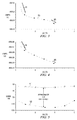
- Figure 3 illustrates an output plot of current verses voltage for the conventional current sink illustrated in Figure 1.
- the saturation region can generally be seen at item 31 and the impact ionization region can be generally seen at item 35.
- the slope of the curve seen at item 33 illustrates the error.
- Figure 4 illustrates an output plot of current and verses voltage for the circuit design illustrated in Figure 2. Notice in the impact ionization 35 of Figure 3 is almost completely cancelled. Also, notice the slope between saturation 31 and impact ionization 35 is at a lower level and much more flat.
- Figure 5 generally shows the derivative of the plots shown in Figures 3 and 4.
- the plots show the impedance in ohms versus voltage for the conventional current sink illustrated in Figure 1 (shown by item 51) and the circuit design illustrated in Figure 2 (shown by item 53). Note that an improvement of approximately a ten fold is made in the impedance.
Landscapes
- Engineering & Computer Science (AREA)
- Microelectronics & Electronic Packaging (AREA)
- Physics & Mathematics (AREA)
- Nonlinear Science (AREA)
- Electromagnetism (AREA)
- General Physics & Mathematics (AREA)
- Radar, Positioning & Navigation (AREA)
- Automation & Control Theory (AREA)
- Amplifiers (AREA)
Abstract
Description
Claims (16)
- A method for increasing output impedance of a current source/sink which includes circuitry for providing an output current to an external load, said circuitry including a first bipolar junction transistor (BJT) having a base, collector and emitter, said first BJT coupled in series with a second BJT having a base, collector and emitter, wherein said emitter of said first BJT is coupled to said collector of said second BJT and the external load is coupled between said collector of said first BJT and said emitter of said second BJT, said method comprising:detecting base current variance in said first BJT; andcompensating for said detected base current variance by applying a current to said first BJT emitter and said second BJT corresponding to the detected base current variation.
- The method of Claim 1 further including applying a constant current to said first BJT base and an emitter of a third BJT also having a base and a collector, said third BJT base is coupled to said second BJT base, and said third BJT collector is coupled to said first BJT emitter.
- The method of Claim 2 further including applying said compensation current via said third BJT collector to said first BJT emitter responsive to variation in the base current of said first BIT.
- The method of any of Claims 1 - 3, wherein said compensation current is approximately equal to the base current error.
- The method of any of Claims 1 - 4, further including varying said compensation current to correspond to variation in the base current of said first BJT due to variations in the external load voltage.
- The method of any of Claims 1 - 5, further compensating for said first BJT base current variance due to beta and impact ionization of said first BJT and due to variation of the external load.
- A device for increasing output impedance of a current amplifier which provides a current to an external load, the current amplifier having an input stage and an output stage, the output stage including a cascode transistor having a base, collector and emitter in cascode with an output transistor having a base, collector and emitter, the device comprising:a means for detecting base current variance in said cascode transistor; anda means for compensating for said detected base current variance by applying a variable current to the cascode transistor emitter and the output transistor collector, said variable current corresponding to the detected base current variation.
- The device of Claim 7, wherein said means for detecting includes means for detecting variation in the base current of said cascode transistor due to Beta and impact ionization of said cascode transistor and due to variation in the external load voltage.
- The device of either Claim 7 or 8, wherein said means for detecting comprises a node for receiving a constant current, wherein said node sources the base current of said cascode transistor and said means for compensating such that when the cascode transistor base current increases, current to the means for compensating decreases by a corresponding amount, and when the base current decreases, current to the means for compensating increases by a corresponding amount.
- The device of Claim 9, wherein said means for compensating comprises a bipolar junction transistor having a base, collector and emitter, wherein said emitter is coupled to said node and said collector is coupled to said output transistor for applying an additive current which directly corresponds to base current increase and base current decrease of said cascode transistor.
- A current amplifier comprising:an input stage for providing a reference current; andan output stage having first circuitry operable to source an output current to an external load, said circuitry including a first bipolar junction transistor (BJT) having a base, collector and emitter, said first BJT coupled in series with a second BJT having a base, collector and emitter, wherein said emitter of said first BJT is coupled to said collector of said second BJT and the external load is coupled between said collector of said first BJT and said emitter of said second BJT;said output stage further having second circuitry coupled to said first BJT and said second BJT and operable to compensate for base current error in said first BJT by directing a current corresponding to the base current error to said first BJT transistor emitter
- The current amplifier of Claim 11, wherein said second circuitry includes a current source operable for applying a constant current and coupled to said first BJT base and an emitter of a third BJT also having a base and a collector, said third BJT base is coupled to said second BJT base, and said third BJT collector is coupled to said first BJT emitter.
- The current amplifier of Claim 12, wherein said third BJT collector applies said compensation current to said first BJT emitter responsive to variation in the base current of said first BJT.
- The current amplifier of any of Claims 11 - 13, wherein said compensation current is approximately equal to the base current error.
- The current amplifier of any of Claims 11 - 14, wherein said second circuitry is further operable to vary said compensation current to correspond to variation in the base current error due to variations in the external load voltage.
- The current amplifier of any of Claims 11 - 15, wherein said second circuitry is further operable to compensate for the base current error due to beta and impact ionization of said first BJT and due to variation of the external load.
Applications Claiming Priority (2)
| Application Number | Priority Date | Filing Date | Title |
|---|---|---|---|
| US10/447,176 US6856188B2 (en) | 2003-05-28 | 2003-05-28 | Current source/sink with high output impedance using bipolar transistors |
| US447176 | 2003-05-28 |
Publications (3)
| Publication Number | Publication Date |
|---|---|
| EP1482391A2 true EP1482391A2 (en) | 2004-12-01 |
| EP1482391A3 EP1482391A3 (en) | 2005-02-09 |
| EP1482391B1 EP1482391B1 (en) | 2007-04-18 |
Family
ID=33131584
Family Applications (1)
| Application Number | Title | Priority Date | Filing Date |
|---|---|---|---|
| EP04102407A Expired - Lifetime EP1482391B1 (en) | 2003-05-28 | 2004-05-28 | A current source/sink with high output impedance using bipolar transistors |
Country Status (4)
| Country | Link |
|---|---|
| US (1) | US6856188B2 (en) |
| EP (1) | EP1482391B1 (en) |
| JP (1) | JP2004357299A (en) |
| DE (1) | DE602004005919T2 (en) |
Families Citing this family (2)
| Publication number | Priority date | Publication date | Assignee | Title |
|---|---|---|---|---|
| US7925320B2 (en) * | 2006-03-06 | 2011-04-12 | Garmin Switzerland Gmbh | Electronic device mount |
| RU2571400C1 (en) * | 2014-10-30 | 2015-12-20 | Федеральное Государственное Бюджетное Образовательное Учреждение Высшего Профессионального Образования "Донской Государственный Технический Университет" (Дгту) | Cascode amplifier with extended frequency band |
Family Cites Families (7)
| Publication number | Priority date | Publication date | Assignee | Title |
|---|---|---|---|---|
| US3843933A (en) * | 1973-04-06 | 1974-10-22 | Rca Corp | Current amplifier |
| US4297646A (en) * | 1980-01-25 | 1981-10-27 | Motorola Inc. | Current mirror circuit |
| US4345217A (en) * | 1980-08-05 | 1982-08-17 | Motorola, Inc. | Cascode current source |
| US4855618A (en) * | 1988-02-16 | 1989-08-08 | Analog Devices, Inc. | MOS current mirror with high output impedance and compliance |
| US5512815A (en) * | 1994-05-09 | 1996-04-30 | National Semiconductor Corporation | Current mirror circuit with current-compensated, high impedance output |
| US5592076A (en) * | 1995-07-03 | 1997-01-07 | Motorola, Inc. | Base current supply circuit for multiple current sources |
| US6664842B1 (en) * | 2001-12-28 | 2003-12-16 | Inphi Corporation | FET active load and current source |
-
2003
- 2003-05-28 US US10/447,176 patent/US6856188B2/en not_active Expired - Lifetime
-
2004
- 2004-05-27 JP JP2004157618A patent/JP2004357299A/en not_active Ceased
- 2004-05-28 EP EP04102407A patent/EP1482391B1/en not_active Expired - Lifetime
- 2004-05-28 DE DE602004005919T patent/DE602004005919T2/en not_active Expired - Lifetime
Also Published As
| Publication number | Publication date |
|---|---|
| US20040239410A1 (en) | 2004-12-02 |
| DE602004005919T2 (en) | 2008-01-17 |
| EP1482391B1 (en) | 2007-04-18 |
| JP2004357299A (en) | 2004-12-16 |
| DE602004005919D1 (en) | 2007-05-31 |
| US6856188B2 (en) | 2005-02-15 |
| EP1482391A3 (en) | 2005-02-09 |
Similar Documents
| Publication | Publication Date | Title |
|---|---|---|
| US8222955B2 (en) | Compensated bandgap | |
| JP2005512376A (en) | Amplifier with bias compensation using a current mirror circuit | |
| US11539337B2 (en) | Amplifier with input bias current cancellation | |
| US12405623B2 (en) | Amplifier having transconductance attenuation | |
| US7233209B2 (en) | Integrated preamplifier circuit for detecting a signal current from a photodiode | |
| US6194886B1 (en) | Early voltage and beta compensation circuit for a current mirror | |
| US6657496B2 (en) | Amplifier circuit with regenerative biasing | |
| US20040056721A1 (en) | Bias circuit with controlled temperature dependence | |
| US6856188B2 (en) | Current source/sink with high output impedance using bipolar transistors | |
| US8760220B1 (en) | Beta enhanced voltage reference circuit | |
| US20240072801A1 (en) | Push-pull buffer circuit | |
| US5973564A (en) | Operational amplifier push-pull output stage with low quiescent current | |
| US20110316635A1 (en) | Triplet transconductor | |
| US4524330A (en) | Bipolar circuit for amplifying differential signal | |
| US6680651B2 (en) | Current mirror and differential amplifier for providing large current ratio and high output impedence | |
| CN115001412A (en) | Self-adaptive bias circuit | |
| US20050264365A1 (en) | Linearity enhanced amplifier | |
| US20260025103A1 (en) | Frequency compensation in amplifiers with local-feedback buffer stages | |
| US20250309845A1 (en) | Amplifier with impedance-setting circuit | |
| EP0508711B1 (en) | Transistor direct-coupled amplifier | |
| US20250047252A1 (en) | Single-ended amplifier with bias stabilization | |
| JP3255226B2 (en) | Voltage controlled amplifier | |
| JP2003316454A (en) | Stabilized power supply circuit | |
| JP3134343B2 (en) | Bandgap reference voltage generation circuit | |
| US20230069204A1 (en) | Control of base currents for output driver transistors in amplifiers |
Legal Events
| Date | Code | Title | Description |
|---|---|---|---|
| PUAI | Public reference made under article 153(3) epc to a published international application that has entered the european phase |
Free format text: ORIGINAL CODE: 0009012 |
|
| AK | Designated contracting states |
Kind code of ref document: A2 Designated state(s): AT BE BG CH CY CZ DE DK EE ES FI FR GB GR HU IE IT LI LU MC NL PL PT RO SE SI SK TR |
|
| AX | Request for extension of the european patent |
Extension state: AL HR LT LV MK |
|
| PUAL | Search report despatched |
Free format text: ORIGINAL CODE: 0009013 |
|
| AK | Designated contracting states |
Kind code of ref document: A3 Designated state(s): AT BE BG CH CY CZ DE DK EE ES FI FR GB GR HU IE IT LI LU MC NL PL PT RO SE SI SK TR |
|
| AX | Request for extension of the european patent |
Extension state: AL HR LT LV MK |
|
| 17P | Request for examination filed |
Effective date: 20050809 |
|
| AKX | Designation fees paid |
Designated state(s): DE FR GB |
|
| GRAP | Despatch of communication of intention to grant a patent |
Free format text: ORIGINAL CODE: EPIDOSNIGR1 |
|
| GRAS | Grant fee paid |
Free format text: ORIGINAL CODE: EPIDOSNIGR3 |
|
| GRAA | (expected) grant |
Free format text: ORIGINAL CODE: 0009210 |
|
| AK | Designated contracting states |
Kind code of ref document: B1 Designated state(s): DE FR GB |
|
| REF | Corresponds to: |
Ref document number: 602004005919 Country of ref document: DE Date of ref document: 20070531 Kind code of ref document: P |
|
| RIN2 | Information on inventor provided after grant (corrected) |
Inventor name: KINYUA, MARTIN KITHINJI Inventor name: CORSI, MARCO Inventor name: BRIGHT, WILLIAM J. |
|
| ET | Fr: translation filed | ||
| PLBE | No opposition filed within time limit |
Free format text: ORIGINAL CODE: 0009261 |
|
| STAA | Information on the status of an ep patent application or granted ep patent |
Free format text: STATUS: NO OPPOSITION FILED WITHIN TIME LIMIT |
|
| 26N | No opposition filed |
Effective date: 20080121 |
|
| PG25 | Lapsed in a contracting state [announced via postgrant information from national office to epo] |
Ref country code: FR Free format text: LAPSE BECAUSE OF NON-PAYMENT OF DUE FEES Effective date: 20070531 |
|
| REG | Reference to a national code |
Ref country code: FR Ref legal event code: PLFP Year of fee payment: 13 |
|
| REG | Reference to a national code |
Ref country code: FR Ref legal event code: PLFP Year of fee payment: 14 |
|
| REG | Reference to a national code |
Ref country code: FR Ref legal event code: PLFP Year of fee payment: 15 |
|
| PGFP | Annual fee paid to national office [announced via postgrant information from national office to epo] |
Ref country code: DE Payment date: 20190412 Year of fee payment: 16 |
|
| PGFP | Annual fee paid to national office [announced via postgrant information from national office to epo] |
Ref country code: FR Payment date: 20190417 Year of fee payment: 16 |
|
| PGFP | Annual fee paid to national office [announced via postgrant information from national office to epo] |
Ref country code: GB Payment date: 20190430 Year of fee payment: 16 |
|
| REG | Reference to a national code |
Ref country code: DE Ref legal event code: R119 Ref document number: 602004005919 Country of ref document: DE |
|
| GBPC | Gb: european patent ceased through non-payment of renewal fee |
Effective date: 20200528 |
|
| PG25 | Lapsed in a contracting state [announced via postgrant information from national office to epo] |
Ref country code: GB Free format text: LAPSE BECAUSE OF NON-PAYMENT OF DUE FEES Effective date: 20200528 Ref country code: FR Free format text: LAPSE BECAUSE OF NON-PAYMENT OF DUE FEES Effective date: 20200531 |
|
| PG25 | Lapsed in a contracting state [announced via postgrant information from national office to epo] |
Ref country code: DE Free format text: LAPSE BECAUSE OF NON-PAYMENT OF DUE FEES Effective date: 20201201 |