EP1482289A1 - Bolomètre à antenne pour ondes millimétriques ou submillimétriques comportant une cavité optimisée et son procédé de fabrication - Google Patents
Bolomètre à antenne pour ondes millimétriques ou submillimétriques comportant une cavité optimisée et son procédé de fabrication Download PDFInfo
- Publication number
- EP1482289A1 EP1482289A1 EP04102263A EP04102263A EP1482289A1 EP 1482289 A1 EP1482289 A1 EP 1482289A1 EP 04102263 A EP04102263 A EP 04102263A EP 04102263 A EP04102263 A EP 04102263A EP 1482289 A1 EP1482289 A1 EP 1482289A1
- Authority
- EP
- European Patent Office
- Prior art keywords
- bolometer
- antenna
- cavity
- silicon
- substrate
- Prior art date
- Legal status (The legal status is an assumption and is not a legal conclusion. Google has not performed a legal analysis and makes no representation as to the accuracy of the status listed.)
- Granted
Links
Images



Classifications
-
- G—PHYSICS
- G01—MEASURING; TESTING
- G01J—MEASUREMENT OF INTENSITY, VELOCITY, SPECTRAL CONTENT, POLARISATION, PHASE OR PULSE CHARACTERISTICS OF INFRARED, VISIBLE OR ULTRAVIOLET LIGHT; COLORIMETRY; RADIATION PYROMETRY
- G01J5/00—Radiation pyrometry, e.g. infrared or optical thermometry
- G01J5/02—Constructional details
- G01J5/08—Optical arrangements
-
- G—PHYSICS
- G01—MEASURING; TESTING
- G01J—MEASUREMENT OF INTENSITY, VELOCITY, SPECTRAL CONTENT, POLARISATION, PHASE OR PULSE CHARACTERISTICS OF INFRARED, VISIBLE OR ULTRAVIOLET LIGHT; COLORIMETRY; RADIATION PYROMETRY
- G01J5/00—Radiation pyrometry, e.g. infrared or optical thermometry
- G01J5/02—Constructional details
- G01J5/08—Optical arrangements
- G01J5/0837—Microantennas, e.g. bow-tie
-
- G—PHYSICS
- G01—MEASURING; TESTING
- G01J—MEASUREMENT OF INTENSITY, VELOCITY, SPECTRAL CONTENT, POLARISATION, PHASE OR PULSE CHARACTERISTICS OF INFRARED, VISIBLE OR ULTRAVIOLET LIGHT; COLORIMETRY; RADIATION PYROMETRY
- G01J5/00—Radiation pyrometry, e.g. infrared or optical thermometry
- G01J5/10—Radiation pyrometry, e.g. infrared or optical thermometry using electric radiation detectors
- G01J5/20—Radiation pyrometry, e.g. infrared or optical thermometry using electric radiation detectors using resistors, thermistors or semiconductors sensitive to radiation, e.g. photoconductive devices
Definitions
- the present invention relates to a bolometric antenna detection device, for millimetric electromagnetic waves or sub-millimeters and a manufacturing process of this device.
- the invention relates to a antenna bolometers matrix for adaptation to the absorption of millimetric electromagnetic waves or submillimetric.
- the invention thus relates to the field of passive bolometric detection, in the range spectral ranging from wavelengths submillimetric at millimeter wavelengths.
- Bolometers measure the power of incident radiation: these are detectors quadratic.
- an absorbing element converts incident light flux into a stream heat, which causes the rise in temperature of a sensitive element, with respect to a temperature of reference.
- a thermometric sensor converts these temperature variations in electrical signals.
- a bolometer is a sensitive detector on a very large spectral band
- the different existing absorption systems are optimized for a certain restricted band.
- the invention relates to a system for designing matrices of bolometers that are easily adaptable to different spectral bands in the field of the invention and provide an improvement notable in terms of photometric performance.
- the submillimeter domain relates to applications of astrophysical observations either spaceborne, airborne or made with the help of telescopes placed on the ground.
- the millimeter domain concerns no only observation applications astrophysics but also military applications or civil.
- detection requires very high performance in terms of detectable power equivalent to noise, this power being in the range of 10 -17 to 10 -15 W / Hz 1/2 .
- Obtaining such performance requires sensors cooled to very low temperature (of the order of 0.3K for bolometers).
- NEPs or noise equivalent powers, in the range of 10 -14 to 10 -12 W / Hz. 1/2 but in a detector temperature range of 150 to 300K, in particular for operational and cost reasons.
- matrix detectors comprising lines and columns of elementary detectors that enable rapid imaging, for example compared to a single-detector system and scan to two dimensions.
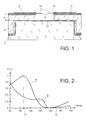
- Figure 1 is a sectional view schematic of a known example of a bolometer millimeter to antenna.
- Such a bolometer comprises a substrate 2 which is metallized and a detection part 4 that is engraved ("etched"), as seen in Figure 1.
- This detection part comprises an antenna 6 as well that a central thermometer 8 that is attached to the antenna 6 through beams or arms 10 of a metal resistive.
- a resonant cavity 12 constituting a quarter-wave cavity, is formed by embedding the substrate 2 in the detection part 4.
- This cavity 12 is made reflective by the metallization 14 of the substrate.
- the thickness or height e of the cavity 12, which is equal to the distance between the antenna 6 and the metallization 14, is adapted to the detection of a radiation of determined wavelength ⁇ : it is worth ⁇ / (4n), where n is the optical index of the material of the detection portion 4, which delimits the cavity 12.
- this material is silicon.
- the value of the resistance of the electric load ("load") of an antenna constituted by the suspension arms of the central thermometer, is too much limited to get maximum absorption of the flow of incident radiation.
- this charge also constitutes the thermal resistance of the bolometer, one is forced to a valuable answer relatively low from this bolometer.
- Such a bolometer has a cavity under its antenna to improve its absorption response. Conventionally, this cavity has an equal thickness a quarter of the average wavelength of radiation that we want to detect.
- This cavity is therefore adapted to a given wavelength. In this way, the signals that are directly absorbed and those who have crossed the cavity add to the output and increase the absorption total.
- the load resistance of this medium is equal to Z 0 / n, where Z 0 is the vacuum impedance (" vacuum ”) which is 377 ⁇ .
- the load resistance R can therefore be at most Z 0 if the material is the vacuum, knowing that it is very difficult to have a vacuum because the antennas are rarely self-supporting.
- the present invention aims to increase the performance of known antenna bolometers and, more especially, to improve the load resistance such bolometers, so as to obtain a weak thermal conductance without degrading the absoption of radiation by these bolometers.
- One solution would be to find a sub-antenna material whose optical index would be less than 1, which is impossible. Must therefore find a way for the "apparent" index (seen by the incident wave) is less than 1. For this, according to the invention, one uses no longer a quarter-wave cavity but a cavity of greater thickness low.
- the invention constitutes, in particular a refinement of the detector bolometric antenna, known from the document [2].
- the present invention has for object a bolometric detection device millimetric electromagnetic waves or submillimeter, this device comprising at least one bolometer having a receiving antenna, a load resistive ("resistive load”), an element thermometer and a resonant cavity, surrounded by part of the bolometer, this part being made of a material having an optical index n, the antenna receiver being located above the cavity resonant, this device being characterized in that the thickness of the resonant cavity is strictly less than ⁇ / (4n), where ⁇ is the wavelength average electromagnetic waves intended to be detected by the device.
- this device comprising at least one bolometer having a receiving antenna, a load resistive (“resistive load”), an element thermometer and a resonant cavity, surrounded by part of the bolometer, this part being made of a material having an optical index n, the antenna receiver being located above the cavity resonant, this device being characterized in that the thickness of the resonant cavity is strictly less than ⁇
- the bolometer comprises further a detection part, which includes the receiving antenna and the thermometric element, and a reflector substrate that is embedded in this part of detection, the resonant cavity being delimited by this reflective substrate and this detection part.
- the receiving antenna is for example a Quadrupole antenna.
- the bolometer can be of cooled type or, on the contrary, uncooled type.
- the device which is the subject of the invention comprises preferably a matrix of MxN bolometers, M and N being integers at least equal to 1.
- the present invention also relates to a manufacturing process of the device object of the invention, in which the bolometer is formed comprising the receiving antenna, the resistive load, the thermometric element and the resonant cavity, from a substrate comprising a structure of solid silicon ("bulk") / silica / thin layer of silicon.
- this substrate comprises a solid silicon / silica / thin layer structure silicon / silica / thin layer of silicon.
- the bolometric device object of the invention comprises a receiving antenna Quadrupole whose topology, resonant cavity and the resistive load are all optimized.
- the step of this antenna is worth 1.6 mm and we use a cavity resonant void 0.5 mm thick.
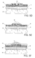
- Variations resulting from the absorption power P (in joules) according to the frequency f (in GHz) are plotted on Figure 2 for a resistive load of 200 ⁇ (curve I) and for a resistive load of 1500 ⁇ (curve II).
- the quarter-wave cavity does not have preponderant effect: there is another effect of resonance, namely a surface wave excitation.
- the thickness the cavity is smaller: it is 0.2 mm; the antenna still has the quadrupole structure but with a pitch of 1.28 mm.
- the results of this simulation are given in Figure 3, for a load of 750 ⁇ (curve I) and for a load of 1500 ⁇ (curve II).
- the difficulty of manufacturing a empty cavity, having for example a thickness of 200 microns, by minimizing the thickness of the silicon under the antenna is bypassed if, instead of using a substrate of SOI type (bulk silicon) / silica / layer thin silicon), a substrate of the type double SOI, also called DSOI substrate (solid silicon / silica / thin layer of silicon (usually a few micrometers thick) / silica / thin layer of silicon).
- SOI type bulk silicon
- DSOI substrate solid silicon / silica / thin layer of silicon (usually a few micrometers thick) / silica / thin layer of silicon).
- the thickness of silicon is thus controlled, regardless of the etching dispersion ("Etching") deep through the back side of the substrate, under an antenna of millimeter size, so as to guarantee the flatness of this antenna and avoid the effect of "folded sheet” resulting from a constraint of the metal layer used for the formation of the antenna.
- the bolometer of Figure 4 includes a silicon substrate 16 and part of detection 18 which is formed from silicon.
- the substrate 16 is fitted in this part 18, by the back side of it.
- This substrate 16 which is view of the detection part 18, is coated with a electrically conductive thin layer 20 constituting a reflector.
- the detection portion 18 includes a antenna 22, for example of quadrupole type, and a central thermometer 24 which is suspended at the antenna by beams 26 made of a resistive metal.
- the bolometer of Figure 4 also includes a resonant cavity 28 which is empty and constituted by the space between the detection part 18 and the reflector 20.
- the antenna 22 is located above this cavity 28.
- the thickness e of the latter is the distance between the antenna 22 and the reflector 20. According to the invention, this thickness e is strictly less than ⁇ / (4n) where ⁇ is the length average wave radiation that we want to detect with the bolometer and n is the optical index of the material which delimits the cavity (here the silicon of the part of detection).
- the detection portion 18 has a first silicon layer 30 of some micrometers thick, which guarantees the mechanical strength of the antenna on the underlying empty cavity, whose height is adjustable thanks to reflecting substrate 16 which is movable.
- the detection part also has a second layer of silicon 32 a few tenths of thickness micrometer, which serves for the realization of the thermometer 18.
- the latter is suspended by the beams 26 made of a resistive metal, for example TiN or TaN.
- the metal that constitutes the beams of suspension 26 becomes superconductor below some Kelvin. So at a temperature of a few tenths of Kelvin, the beams have a very high thermal resistance.
- a substrate 34 (FIG. 5A) is used which constitutes a DSOI substrate.
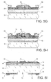
- mesa etching we eliminate most of the silicon of zones 48 and 50 and underlying silicon doped p ++ these areas to basically let subsist zone 52 as seen in Figure 5C.
- a layer 58 of silica whose thickness is for example 1 ⁇ m, then, on this layer 58, a layer 60 of photosensitive resin, for example a 5730 resin layer (Shipley Company) of 7 ⁇ m thick.
- a layer 66 of reflective metal on the obtained structure for example a 400nm gold layer thick.
- This layer will be used for the formation of the bolometer antenna.
- both ends of it then remains a layer 72 of TEOS silica, for example, 1 ⁇ m thick, and narrow width, for example 50nm.
- a layer 72 of TEOS silica for example, 1 ⁇ m thick, and narrow width, for example 50nm.
- oxide layer 74 obtained by PECVD, 2 ⁇ m thick for example and similarly width as the layer 72.
- a layer of resin photosensitive material 76 for example a layer of resin 5740 of thickness 7 ⁇ m, which extends on both sides of the substrate by covering layers 72 and 74 of low width, while letting appear a part center 78 of the substrate 36 which has been etched on a thin, of the order of 5 .mu.m for example.
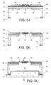
- portions 84 of the silicon of substrate 36 subsist in the areas below the antenna, in continuity with the lateral parts 80 and 82, these portions 84 having a small thickness, the order of 5 ⁇ m.
- a silicon substrate 92 is manufactured which can be embedded in the structure obtained in Figure 5K, by the back side of this structure, as we see in Figure 5L.
- an electrically conductive layer 94 thin, for example a layer of gold of 400 nm thick.
- the quadrupole antenna can be replaced by any other antenna compatible with a such device, for example a spiral antenna.
- Bolometers 98 of this matrix 96 are formed from the same DSOI substrate, on which one provides electrical insulation (not shown) which are necessary for bolometers.
- a reflective substrate is provided 100 for a collective recess in the parts of detection (not shown) of bolometers 98.
Landscapes
- Physics & Mathematics (AREA)
- General Physics & Mathematics (AREA)
- Spectroscopy & Molecular Physics (AREA)
- Photometry And Measurement Of Optical Pulse Characteristics (AREA)
- Radiation Pyrometers (AREA)
- Particle Accelerators (AREA)
- Radar Systems Or Details Thereof (AREA)
- Control Of Motors That Do Not Use Commutators (AREA)
Abstract
Description
- la figure 1 est une vue en coupe schématique d'un bolomètre à antenne connu et a déjà été décrite,
- les figures 2 et 3 montrent des courbes traduisant des résultats de la simulation du comportement électromagnétique de bolomètres à antenne,
- la figure 4 est une vue en coupe schématique d'un exemple de dispositif bolométrique conforme à l'invention,
- les figures 5A à 5L illustrent schématiquement des étapes d'un exemple de procédé de fabrication conforme à l'invention, et
- la figure 6 illustre schématiquement un dispositif bolométrique matriciel conforme à l'invention.
- un substrat de silicium massif (« bulk ») 36, dont l'épaisseur vaut par exemple 450 µm,
- une couche mince de silice enterrée 38, dont l'épaisseur vaut par exemple 380 nm,
- une couche mince de silicium épitaxié 40, dont l'épaisseur vaut par exemple 5µm,
- une autre couche mince de silice enterrée 42, dont l'épaisseur vaut par exemple 380 nm, et
- une autre couche mince de silicium épitaxié 44, dont l'épaisseur vaut par exemple 1µm.
- une première implantation ionique de silicium dopé p++ (référence 46 sur la figure 5B) pour définir trois zones de silicium dans la couche 44, dont les références sont 48, 50 et 52, et
- une deuxième implantation ionique pour former, dans la zone centrale 52, une zone 54 de silicium dopé n++, dont l'épaisseur vaut par exemple 500 nanomètres.
Claims (8)
- Dispositif de détection bolométrique d'ondes électromagnétiques millimétriques ou submillimétriques, ce dispositif comprenant au moins un 5 bolomètre comportant une antenne réceptrice (22, 68), une charge résistive (26, 90), un élément thermométrique (24, 88) et une cavité résonante (28), entourée par une partie du bolomètre, cette partie étant faite d'un matériau ayant un indice optique n, l'antenne réceptrice étant située au-dessus de la cavité résonante, ce dispositif étant caractérisé en ce que l'épaisseur de la cavité résonante est strictement inférieure à λ/(4n), où λ est la longueur d'onde moyenne des ondes électromagnétiques destinées à être 5 détectées par le dispositif.
- Dispositif selon la revendication 1, dans lequel le bolomètre comprend en outre une partie de détection (18), qui comprend l'antenne réceptrice (22) et l'élément thermométrique (24), et un substrat réflecteur (16, 92) qui est encastré dans cette partie de détection, la cavité résonante étant délimitée par ce substrat réflecteur et cette partie de détection.
- Dispositif selon l'une quelconque des revendications 1 et 2, dans lequel l'antenne réceptrice 5 est une antenne quadrupolaire (22, 68).
- Dispositif selon l'une quelconque des revendications 1 à 3, dans lequel le bolomètre est de type refroidi.
- Dispositif selon l'une quelconque des revendications 1 à 3, dans lequel le bolomètre est de type non refroidi.
- Dispositif selon l'une quelconque des revendications 1 à 5, comprenant une matrice (96) de MxN bolomètres, M et N étant des entiers au moins égaux à 1.
- Procédé de fabrication du dispositif selon l'une quelconque des revendications 1 à 6, dans lequel on forme le bolomètre comportant l'antenne réceptrice (68), la charge résistive (90), l'élément thermométrique (88) et la cavité résonante, à partir d'un substrat (34) comprenant une structure de silicium massif/silice/couche mince de silicium.
- Procédé selon la revendication 7, dans lequel le substrat (34) comprend une structure de silicium massif/silice/couche mince de silicium/silice/couche mince de silicium.
Applications Claiming Priority (2)
| Application Number | Priority Date | Filing Date | Title |
|---|---|---|---|
| FR0350176A FR2855609B1 (fr) | 2003-05-26 | 2003-05-26 | Dispositif de detection bolometrique a antenne, a cavite optimisee, pour ondes electromagnetiques millimetriques ou submillimetriques, et procede de fabrication de ce dispositif |
| FR0350176 | 2003-05-26 |
Publications (2)
| Publication Number | Publication Date |
|---|---|
| EP1482289A1 true EP1482289A1 (fr) | 2004-12-01 |
| EP1482289B1 EP1482289B1 (fr) | 2010-06-02 |
Family
ID=33104529
Family Applications (1)
| Application Number | Title | Priority Date | Filing Date |
|---|---|---|---|
| EP04102263A Expired - Lifetime EP1482289B1 (fr) | 2003-05-26 | 2004-05-24 | Procédé de détection bolométrique pour ondes (sub-)millimétriques utilisant un bolomètre à antenne ayant une cavité |
Country Status (6)
| Country | Link |
|---|---|
| US (1) | US6985116B2 (fr) |
| EP (1) | EP1482289B1 (fr) |
| JP (1) | JP4571433B2 (fr) |
| AT (1) | ATE470135T1 (fr) |
| DE (1) | DE602004027441D1 (fr) |
| FR (1) | FR2855609B1 (fr) |
Cited By (1)
| Publication number | Priority date | Publication date | Assignee | Title |
|---|---|---|---|---|
| MD340Z (ro) * | 2010-04-23 | 2011-09-30 | Институт Электронной Инженерии И Промышленных Технологий | Bolometru |
Families Citing this family (17)
| Publication number | Priority date | Publication date | Assignee | Title |
|---|---|---|---|---|
| FI114658B (fi) * | 2002-06-03 | 2004-11-30 | Metorex Internat Oy | Suprajohtava antennikytketty kuumapistemikrobolometri, menetelmät sellaisen valmistamiseksi ja käyttämiseksi sekä bolometrinen kuvantamisjärjestely |
| US7038623B2 (en) * | 2003-12-04 | 2006-05-02 | Raytheon Company | Method and apparatus for detecting radiation at one wavelength using a detector for a different wavelength |
| FR2884608B1 (fr) | 2005-04-18 | 2007-05-25 | Commissariat Energie Atomique | Detecteur bolometrique, dispositif de detection d'ondes electromagnetiques submillimetriques et millimetriques mettant en oeuvre un tel detecteur |
| JP4221424B2 (ja) | 2006-08-09 | 2009-02-12 | 株式会社東芝 | 固体撮像素子及びその製造方法並びに撮像装置 |
| JP4398972B2 (ja) * | 2006-12-11 | 2010-01-13 | 株式会社東芝 | 電磁波センサ、撮像素子及び撮像装置 |
| JP5597862B2 (ja) * | 2007-03-27 | 2014-10-01 | 日本電気株式会社 | ボロメータ型THz波検出器 |
| JP5219745B2 (ja) * | 2007-11-14 | 2013-06-26 | キヤノン株式会社 | 発光装置 |
| US8130160B2 (en) * | 2008-07-03 | 2012-03-06 | The Boeing Company | Composite dipole array assembly |
| FR2934044B1 (fr) * | 2008-07-17 | 2014-08-15 | Commissariat Energie Atomique | Detecteur bolometrique d'ondes electromagnetiques. |
| FR2945119B1 (fr) * | 2009-04-30 | 2011-04-08 | Commissariat Energie Atomique | Detecteur bolometrique d'un rayonnement electromagnetique dans le domaine du terahertz et dispositif de detection matriciel comportant de tels detecteurs |
| FR2969284B1 (fr) * | 2010-12-17 | 2012-12-14 | Commissariat Energie Atomique | Detecteur infrarouge a base de micro-planches bolometriques suspendues |
| JP5685980B2 (ja) * | 2011-02-23 | 2015-03-18 | セイコーエプソン株式会社 | 熱型光検出器、熱型光検出装置及び電子機器 |
| US9759693B2 (en) * | 2012-12-20 | 2017-09-12 | International Business Machines Corporation | Method of simulating the absorption of plane waves using FEM software tools |
| US20170030775A1 (en) * | 2014-04-18 | 2017-02-02 | Nec Corporation | Terahertz-wave detector |
| US9476774B2 (en) | 2014-12-17 | 2016-10-25 | Institut National D'optique | Uncooled microbolometer pixel and array for configurable broadband and multi-frequency terahertz detection |
| US11217874B2 (en) * | 2019-04-15 | 2022-01-04 | Analog Devices, Inc. | Silicon cavity backed radiator structure |
| FR3101151B1 (fr) * | 2019-09-24 | 2021-12-17 | Office National Detudes Rech Aerospatiales | Dispositif pour reveler des variations spatiales de polarisation d’un rayonnement electromagnetique |
Citations (1)
| Publication number | Priority date | Publication date | Assignee | Title |
|---|---|---|---|---|
| WO2000040937A1 (fr) * | 1998-12-30 | 2000-07-13 | Commissariat A L'energie Atomique | Detecteur bolometrique a antenne |
Family Cites Families (15)
| Publication number | Priority date | Publication date | Assignee | Title |
|---|---|---|---|---|
| US5286976A (en) * | 1988-11-07 | 1994-02-15 | Honeywell Inc. | Microstructure design for high IR sensitivity |
| JPH06317475A (ja) * | 1991-07-19 | 1994-11-15 | Terumo Corp | 赤外線センサおよびその製造方法 |
| DE69313337T2 (de) * | 1992-04-17 | 1998-01-02 | Terumo Corp | Infrarotsensor und Verfahren für dessen Herstellung |
| JP3181363B2 (ja) * | 1992-04-17 | 2001-07-03 | テルモ株式会社 | 赤外線センサおよびその製造方法 |
| US5572060A (en) * | 1995-02-01 | 1996-11-05 | Southern Methodist University | Uncooled YBaCuO thin film infrared detector |
| FR2735574B1 (fr) | 1995-06-15 | 1997-07-18 | Commissariat Energie Atomique | Dispositif de detection bolometrique pour ondes millimetriques et submillimetriques et procede de fabrication de ce dispositif |
| FR2752299B1 (fr) | 1996-08-08 | 1998-09-11 | Commissariat Energie Atomique | Detecteur infrarouge et procede de fabication de celui-ci |
| FR2773215B1 (fr) | 1997-12-31 | 2000-01-28 | Commissariat Energie Atomique | Detecteur thermique bolometrique |
| JPH11344377A (ja) * | 1998-06-02 | 1999-12-14 | Matsushita Electric Ind Co Ltd | 赤外線検知素子およびその製造方法 |
| FR2780784B1 (fr) | 1998-07-06 | 2000-08-11 | Commissariat Energie Atomique | Detecteur thermique a amplification par effet bolometrique |
| US6329655B1 (en) | 1998-10-07 | 2001-12-11 | Raytheon Company | Architecture and method of coupling electromagnetic energy to thermal detectors |
| FR2796148B1 (fr) | 1999-07-08 | 2001-11-23 | Commissariat Energie Atomique | Detecteur bolometrique a isolation electrique intermediaire et procede de fabrication de ce detecteur |
| US6300554B1 (en) * | 1999-09-09 | 2001-10-09 | Metrodyne Microsystem Corp. | Method of fabricating thermoelectric sensor and thermoelectric sensor device |
| US6292140B1 (en) * | 1999-11-03 | 2001-09-18 | Hypres, Inc. | Antenna for millimeter-wave imaging and bolometer employing the antenna |
| FI114658B (fi) * | 2002-06-03 | 2004-11-30 | Metorex Internat Oy | Suprajohtava antennikytketty kuumapistemikrobolometri, menetelmät sellaisen valmistamiseksi ja käyttämiseksi sekä bolometrinen kuvantamisjärjestely |
-
2003
- 2003-05-26 FR FR0350176A patent/FR2855609B1/fr not_active Expired - Fee Related
-
2004
- 2004-05-06 US US10/839,129 patent/US6985116B2/en not_active Expired - Lifetime
- 2004-05-24 AT AT04102263T patent/ATE470135T1/de not_active IP Right Cessation
- 2004-05-24 DE DE602004027441T patent/DE602004027441D1/de not_active Expired - Lifetime
- 2004-05-24 EP EP04102263A patent/EP1482289B1/fr not_active Expired - Lifetime
- 2004-05-25 JP JP2004155269A patent/JP4571433B2/ja not_active Expired - Fee Related
Patent Citations (1)
| Publication number | Priority date | Publication date | Assignee | Title |
|---|---|---|---|---|
| WO2000040937A1 (fr) * | 1998-12-30 | 2000-07-13 | Commissariat A L'energie Atomique | Detecteur bolometrique a antenne |
Cited By (1)
| Publication number | Priority date | Publication date | Assignee | Title |
|---|---|---|---|---|
| MD340Z (ro) * | 2010-04-23 | 2011-09-30 | Институт Электронной Инженерии И Промышленных Технологий | Bolometru |
Also Published As
| Publication number | Publication date |
|---|---|
| JP4571433B2 (ja) | 2010-10-27 |
| US20040252065A1 (en) | 2004-12-16 |
| ATE470135T1 (de) | 2010-06-15 |
| FR2855609A1 (fr) | 2004-12-03 |
| JP2004354380A (ja) | 2004-12-16 |
| DE602004027441D1 (de) | 2010-07-15 |
| EP1482289B1 (fr) | 2010-06-02 |
| FR2855609B1 (fr) | 2005-07-01 |
| US6985116B2 (en) | 2006-01-10 |
Similar Documents
| Publication | Publication Date | Title |
|---|---|---|
| EP1482289B1 (fr) | Procédé de détection bolométrique pour ondes (sub-)millimétriques utilisant un bolomètre à antenne ayant une cavité | |
| EP2095467B1 (fr) | Antenne et emetteur/recepteur terahertz integres, et procede pour leur fabrication. | |
| EP2450681B1 (fr) | Détecteur infrarouge a base de micro-planches bolométriques suspendues | |
| EP1715315B1 (fr) | Détecteur bolométrique, dispositif de détection d'ondes électromagnétiques submillimétriques et millimétriques mettant en oeuvre un tel détecteur | |
| EP1909080B1 (fr) | Détecteur optique ultrasensible à grande résolution temporelle, utilisant un couplage à réseau | |
| EP2340422A1 (fr) | Detecteur bolometrique d'ondes electromagnetiques | |
| FR2977937A1 (fr) | Detecteur bolometrique a performances ameliorees | |
| EP0971219A1 (fr) | Détecteur thermique à amplification par effet bolomètrique | |
| EP2466283A1 (fr) | Détecteur infrarouge à base de micro-planches bolométriques suspendues | |
| FR2735574A1 (fr) | Dispositif de detection bolometrique pour ondes millimetriques et submillimetriques et procede de fabrication de ce dispositif | |
| EP3999826B1 (fr) | Micro-bolomètre a faible capacité thermique et procédé de fabrication associé | |
| EP3806167A1 (fr) | Procede de fabrication d'au moins une photodiode planaire contrainte en tension | |
| EP2019301B1 (fr) | Détecteur de rayonnement électromagnétique et procédé de fabrication d'un tel détecteur | |
| EP1147389B1 (fr) | Detecteur bolometrique a antenne | |
| EP1880176A1 (fr) | Detecteur thermique de rayonnements electromagnetiques et dispositif de detection infrarouge mettant en oeuvre de tels detecteurs | |
| EP1692475B1 (fr) | Dispositif de mesure d energie rayonnante ameliore a deux positions | |
| EP3703138B1 (fr) | Structure de détection de rayonnement électromagnétique à haute efficacité d'absorption et un procédé de fabrication d'une telle structure | |
| FR2997760A1 (fr) | Dispositif de pixels-image et reseau forme de tels dispositifs ainsi que procede de saisie de rayonnement electromagnetique par un tel dispositif | |
| EP4350890A1 (fr) | Commutateur a base d'un materiau a changement de phase | |
| FR3066017B1 (fr) | Dispositif pyroelectrique de detection infrarouge comportant un emetteur infrarouge de modulation | |
| EP4056969B1 (fr) | Detecteur thermique d'un rayonnement electromagnetique comportant une antenne et une charge resistive couplees de maniere inductive | |
| EP2767810A1 (fr) | Procédé de réalisation d'un dispositif imageur | |
| FR2885690A1 (fr) | Detecteur thermique de rayonnements electromagnetiques et dispositif de detection infrarouge mettant en oeuvre de tels detecteurs | |
| EP4542188A1 (fr) | Detecteur thermique comportant un transducteur thermometre a diodes | |
| WO2026046821A1 (fr) | Micro-bolometre comprenant un bras d'isolation thermique ameliore |
Legal Events
| Date | Code | Title | Description |
|---|---|---|---|
| PUAI | Public reference made under article 153(3) epc to a published international application that has entered the european phase |
Free format text: ORIGINAL CODE: 0009012 |
|
| AK | Designated contracting states |
Kind code of ref document: A1 Designated state(s): AT BE BG CH CY CZ DE DK EE ES FI FR GB GR HU IE IT LI LU MC NL PL PT RO SE SI SK TR |
|
| AX | Request for extension of the european patent |
Extension state: AL HR LT LV MK |
|
| 17P | Request for examination filed |
Effective date: 20050524 |
|
| AKX | Designation fees paid |
Designated state(s): AT BE BG CH CY CZ DE DK EE ES FI FR GB GR HU IE IT LI LU MC NL PL PT RO SE SI SK TR |
|
| RAP1 | Party data changed (applicant data changed or rights of an application transferred) |
Owner name: COMMISSARIAT A L'ENERGIE ATOMIQUE |
|
| 17Q | First examination report despatched |
Effective date: 20071001 |
|
| GRAP | Despatch of communication of intention to grant a patent |
Free format text: ORIGINAL CODE: EPIDOSNIGR1 |
|
| RTI1 | Title (correction) |
Free format text: BOLOMETRIC DETECTION METHOD OF (SUB-)MILLIMETER WAVES USING AN ANTENNA COUPLED BOLOMETER HAVING A CAVITY |
|
| GRAS | Grant fee paid |
Free format text: ORIGINAL CODE: EPIDOSNIGR3 |
|
| GRAA | (expected) grant |
Free format text: ORIGINAL CODE: 0009210 |
|
| RAP1 | Party data changed (applicant data changed or rights of an application transferred) |
Owner name: COMMISSARIAT A L'ENERGIE ATOMIQUE ET AUX ENERGIES |
|
| AK | Designated contracting states |
Kind code of ref document: B1 Designated state(s): AT BE BG CH CY CZ DE DK EE ES FI FR GB GR HU IE IT LI LU MC NL PL PT RO SE SI SK TR |
|
| REG | Reference to a national code |
Ref country code: GB Ref legal event code: FG4D Free format text: NOT ENGLISH |
|
| REG | Reference to a national code |
Ref country code: CH Ref legal event code: EP |
|
| REG | Reference to a national code |
Ref country code: IE Ref legal event code: FG4D Free format text: LANGUAGE OF EP DOCUMENT: FRENCH |
|
| REF | Corresponds to: |
Ref document number: 602004027441 Country of ref document: DE Date of ref document: 20100715 Kind code of ref document: P |
|
| REG | Reference to a national code |
Ref country code: NL Ref legal event code: VDEP Effective date: 20100602 |
|
| PG25 | Lapsed in a contracting state [announced via postgrant information from national office to epo] |
Ref country code: SE Free format text: LAPSE BECAUSE OF FAILURE TO SUBMIT A TRANSLATION OF THE DESCRIPTION OR TO PAY THE FEE WITHIN THE PRESCRIBED TIME-LIMIT Effective date: 20100602 |
|
| PG25 | Lapsed in a contracting state [announced via postgrant information from national office to epo] |
Ref country code: AT Free format text: LAPSE BECAUSE OF FAILURE TO SUBMIT A TRANSLATION OF THE DESCRIPTION OR TO PAY THE FEE WITHIN THE PRESCRIBED TIME-LIMIT Effective date: 20100602 Ref country code: SI Free format text: LAPSE BECAUSE OF FAILURE TO SUBMIT A TRANSLATION OF THE DESCRIPTION OR TO PAY THE FEE WITHIN THE PRESCRIBED TIME-LIMIT Effective date: 20100602 Ref country code: FI Free format text: LAPSE BECAUSE OF FAILURE TO SUBMIT A TRANSLATION OF THE DESCRIPTION OR TO PAY THE FEE WITHIN THE PRESCRIBED TIME-LIMIT Effective date: 20100602 |
|
| PG25 | Lapsed in a contracting state [announced via postgrant information from national office to epo] |
Ref country code: CY Free format text: LAPSE BECAUSE OF FAILURE TO SUBMIT A TRANSLATION OF THE DESCRIPTION OR TO PAY THE FEE WITHIN THE PRESCRIBED TIME-LIMIT Effective date: 20100602 Ref country code: GR Free format text: LAPSE BECAUSE OF FAILURE TO SUBMIT A TRANSLATION OF THE DESCRIPTION OR TO PAY THE FEE WITHIN THE PRESCRIBED TIME-LIMIT Effective date: 20100903 Ref country code: PL Free format text: LAPSE BECAUSE OF FAILURE TO SUBMIT A TRANSLATION OF THE DESCRIPTION OR TO PAY THE FEE WITHIN THE PRESCRIBED TIME-LIMIT Effective date: 20100602 |
|
| REG | Reference to a national code |
Ref country code: IE Ref legal event code: FD4D |
|
| PG25 | Lapsed in a contracting state [announced via postgrant information from national office to epo] |
Ref country code: NL Free format text: LAPSE BECAUSE OF FAILURE TO SUBMIT A TRANSLATION OF THE DESCRIPTION OR TO PAY THE FEE WITHIN THE PRESCRIBED TIME-LIMIT Effective date: 20100602 Ref country code: EE Free format text: LAPSE BECAUSE OF FAILURE TO SUBMIT A TRANSLATION OF THE DESCRIPTION OR TO PAY THE FEE WITHIN THE PRESCRIBED TIME-LIMIT Effective date: 20100602 Ref country code: IE Free format text: LAPSE BECAUSE OF FAILURE TO SUBMIT A TRANSLATION OF THE DESCRIPTION OR TO PAY THE FEE WITHIN THE PRESCRIBED TIME-LIMIT Effective date: 20100602 |
|
| PG25 | Lapsed in a contracting state [announced via postgrant information from national office to epo] |
Ref country code: PT Free format text: LAPSE BECAUSE OF FAILURE TO SUBMIT A TRANSLATION OF THE DESCRIPTION OR TO PAY THE FEE WITHIN THE PRESCRIBED TIME-LIMIT Effective date: 20101004 Ref country code: RO Free format text: LAPSE BECAUSE OF FAILURE TO SUBMIT A TRANSLATION OF THE DESCRIPTION OR TO PAY THE FEE WITHIN THE PRESCRIBED TIME-LIMIT Effective date: 20100602 Ref country code: CZ Free format text: LAPSE BECAUSE OF FAILURE TO SUBMIT A TRANSLATION OF THE DESCRIPTION OR TO PAY THE FEE WITHIN THE PRESCRIBED TIME-LIMIT Effective date: 20100602 Ref country code: SK Free format text: LAPSE BECAUSE OF FAILURE TO SUBMIT A TRANSLATION OF THE DESCRIPTION OR TO PAY THE FEE WITHIN THE PRESCRIBED TIME-LIMIT Effective date: 20100602 |
|
| PLBE | No opposition filed within time limit |
Free format text: ORIGINAL CODE: 0009261 |
|
| STAA | Information on the status of an ep patent application or granted ep patent |
Free format text: STATUS: NO OPPOSITION FILED WITHIN TIME LIMIT |
|
| PG25 | Lapsed in a contracting state [announced via postgrant information from national office to epo] |
Ref country code: DK Free format text: LAPSE BECAUSE OF FAILURE TO SUBMIT A TRANSLATION OF THE DESCRIPTION OR TO PAY THE FEE WITHIN THE PRESCRIBED TIME-LIMIT Effective date: 20100602 |
|
| 26N | No opposition filed |
Effective date: 20110303 |
|
| REG | Reference to a national code |
Ref country code: DE Ref legal event code: R097 Ref document number: 602004027441 Country of ref document: DE Effective date: 20110302 |
|
| BERE | Be: lapsed |
Owner name: COMMISSARIAT A L'ENERGIE ATOMIQUE ET AUX ENERGIES Effective date: 20110531 |
|
| PG25 | Lapsed in a contracting state [announced via postgrant information from national office to epo] |
Ref country code: MC Free format text: LAPSE BECAUSE OF NON-PAYMENT OF DUE FEES Effective date: 20110531 |
|
| REG | Reference to a national code |
Ref country code: CH Ref legal event code: PL |
|
| PG25 | Lapsed in a contracting state [announced via postgrant information from national office to epo] |
Ref country code: CH Free format text: LAPSE BECAUSE OF NON-PAYMENT OF DUE FEES Effective date: 20110531 Ref country code: LI Free format text: LAPSE BECAUSE OF NON-PAYMENT OF DUE FEES Effective date: 20110531 |
|
| PG25 | Lapsed in a contracting state [announced via postgrant information from national office to epo] |
Ref country code: BE Free format text: LAPSE BECAUSE OF NON-PAYMENT OF DUE FEES Effective date: 20110531 |
|
| PG25 | Lapsed in a contracting state [announced via postgrant information from national office to epo] |
Ref country code: LU Free format text: LAPSE BECAUSE OF NON-PAYMENT OF DUE FEES Effective date: 20110524 |
|
| PG25 | Lapsed in a contracting state [announced via postgrant information from national office to epo] |
Ref country code: BG Free format text: LAPSE BECAUSE OF FAILURE TO SUBMIT A TRANSLATION OF THE DESCRIPTION OR TO PAY THE FEE WITHIN THE PRESCRIBED TIME-LIMIT Effective date: 20100902 Ref country code: TR Free format text: LAPSE BECAUSE OF FAILURE TO SUBMIT A TRANSLATION OF THE DESCRIPTION OR TO PAY THE FEE WITHIN THE PRESCRIBED TIME-LIMIT Effective date: 20100602 |
|
| PG25 | Lapsed in a contracting state [announced via postgrant information from national office to epo] |
Ref country code: HU Free format text: LAPSE BECAUSE OF FAILURE TO SUBMIT A TRANSLATION OF THE DESCRIPTION OR TO PAY THE FEE WITHIN THE PRESCRIBED TIME-LIMIT Effective date: 20100602 Ref country code: ES Free format text: LAPSE BECAUSE OF FAILURE TO SUBMIT A TRANSLATION OF THE DESCRIPTION OR TO PAY THE FEE WITHIN THE PRESCRIBED TIME-LIMIT Effective date: 20100913 |
|
| REG | Reference to a national code |
Ref country code: FR Ref legal event code: PLFP Year of fee payment: 13 |
|
| REG | Reference to a national code |
Ref country code: FR Ref legal event code: PLFP Year of fee payment: 14 |
|
| REG | Reference to a national code |
Ref country code: FR Ref legal event code: PLFP Year of fee payment: 15 |
|
| PGFP | Annual fee paid to national office [announced via postgrant information from national office to epo] |
Ref country code: DE Payment date: 20180514 Year of fee payment: 15 |
|
| PGFP | Annual fee paid to national office [announced via postgrant information from national office to epo] |
Ref country code: IT Payment date: 20180514 Year of fee payment: 15 Ref country code: FR Payment date: 20180528 Year of fee payment: 15 |
|
| PGFP | Annual fee paid to national office [announced via postgrant information from national office to epo] |
Ref country code: GB Payment date: 20180518 Year of fee payment: 15 |
|
| REG | Reference to a national code |
Ref country code: DE Ref legal event code: R119 Ref document number: 602004027441 Country of ref document: DE |
|
| GBPC | Gb: european patent ceased through non-payment of renewal fee |
Effective date: 20190524 |
|
| PG25 | Lapsed in a contracting state [announced via postgrant information from national office to epo] |
Ref country code: DE Free format text: LAPSE BECAUSE OF NON-PAYMENT OF DUE FEES Effective date: 20191203 Ref country code: GB Free format text: LAPSE BECAUSE OF NON-PAYMENT OF DUE FEES Effective date: 20190524 Ref country code: IT Free format text: LAPSE BECAUSE OF NON-PAYMENT OF DUE FEES Effective date: 20190524 |
|
| PG25 | Lapsed in a contracting state [announced via postgrant information from national office to epo] |
Ref country code: FR Free format text: LAPSE BECAUSE OF NON-PAYMENT OF DUE FEES Effective date: 20190531 |