EP1480272A2 - Organic EL display device, electronic equipment, and method for manufacturing the same - Google Patents
Organic EL display device, electronic equipment, and method for manufacturing the same Download PDFInfo
- Publication number
- EP1480272A2 EP1480272A2 EP04253023A EP04253023A EP1480272A2 EP 1480272 A2 EP1480272 A2 EP 1480272A2 EP 04253023 A EP04253023 A EP 04253023A EP 04253023 A EP04253023 A EP 04253023A EP 1480272 A2 EP1480272 A2 EP 1480272A2
- Authority
- EP
- European Patent Office
- Prior art keywords
- layer
- organic
- substrate
- display device
- laminate
- Prior art date
- Legal status (The legal status is an assumption and is not a legal conclusion. Google has not performed a legal analysis and makes no representation as to the accuracy of the status listed.)
- Withdrawn
Links
- 238000000034 method Methods 0.000 title claims description 29
- 238000004519 manufacturing process Methods 0.000 title claims description 15
- 239000010410 layer Substances 0.000 claims abstract description 152
- 239000000758 substrate Substances 0.000 claims abstract description 135
- 239000010409 thin film Substances 0.000 claims abstract description 41
- 239000010408 film Substances 0.000 claims abstract description 28
- 230000015572 biosynthetic process Effects 0.000 claims abstract description 9
- 239000012790 adhesive layer Substances 0.000 claims abstract description 8
- 238000005304 joining Methods 0.000 claims abstract description 8
- 238000004090 dissolution Methods 0.000 claims description 4
- QVGXLLKOCUKJST-UHFFFAOYSA-N atomic oxygen Chemical compound [O] QVGXLLKOCUKJST-UHFFFAOYSA-N 0.000 abstract description 11
- 239000001301 oxygen Substances 0.000 abstract description 11
- 229910052760 oxygen Inorganic materials 0.000 abstract description 11
- 239000011241 protective layer Substances 0.000 abstract description 11
- VYPSYNLAJGMNEJ-UHFFFAOYSA-N Silicium dioxide Chemical compound O=[Si]=O VYPSYNLAJGMNEJ-UHFFFAOYSA-N 0.000 description 18
- 239000007789 gas Substances 0.000 description 14
- 238000007789 sealing Methods 0.000 description 13
- BLRPTPMANUNPDV-UHFFFAOYSA-N Silane Chemical compound [SiH4] BLRPTPMANUNPDV-UHFFFAOYSA-N 0.000 description 12
- 239000000463 material Substances 0.000 description 12
- 239000000853 adhesive Substances 0.000 description 11
- 230000001070 adhesive effect Effects 0.000 description 11
- 229910021417 amorphous silicon Inorganic materials 0.000 description 10
- 238000005229 chemical vapour deposition Methods 0.000 description 10
- 229920003023 plastic Polymers 0.000 description 8
- 239000004033 plastic Substances 0.000 description 8
- 239000000377 silicon dioxide Substances 0.000 description 8
- 238000010586 diagram Methods 0.000 description 7
- 238000001259 photo etching Methods 0.000 description 7
- 230000008569 process Effects 0.000 description 7
- 235000012239 silicon dioxide Nutrition 0.000 description 7
- 239000011347 resin Substances 0.000 description 6
- 229920005989 resin Polymers 0.000 description 6
- UFHFLCQGNIYNRP-UHFFFAOYSA-N Hydrogen Chemical compound [H][H] UFHFLCQGNIYNRP-UHFFFAOYSA-N 0.000 description 5
- 239000011521 glass Substances 0.000 description 5
- 239000001257 hydrogen Substances 0.000 description 5
- 229910052739 hydrogen Inorganic materials 0.000 description 5
- 239000012535 impurity Substances 0.000 description 5
- OYPRJOBELJOOCE-UHFFFAOYSA-N Calcium Chemical compound [Ca] OYPRJOBELJOOCE-UHFFFAOYSA-N 0.000 description 4
- KRHYYFGTRYWZRS-UHFFFAOYSA-N Fluorane Chemical compound F KRHYYFGTRYWZRS-UHFFFAOYSA-N 0.000 description 4
- XUIMIQQOPSSXEZ-UHFFFAOYSA-N Silicon Chemical compound [Si] XUIMIQQOPSSXEZ-UHFFFAOYSA-N 0.000 description 4
- 229910052791 calcium Inorganic materials 0.000 description 4
- 239000011575 calcium Substances 0.000 description 4
- 230000001413 cellular effect Effects 0.000 description 4
- 230000000052 comparative effect Effects 0.000 description 4
- 239000004020 conductor Substances 0.000 description 4
- 238000005530 etching Methods 0.000 description 4
- 230000003287 optical effect Effects 0.000 description 4
- 229910021420 polycrystalline silicon Inorganic materials 0.000 description 4
- 229910052710 silicon Inorganic materials 0.000 description 4
- 239000010703 silicon Substances 0.000 description 4
- QGZKDVFQNNGYKY-UHFFFAOYSA-N Ammonia Chemical compound N QGZKDVFQNNGYKY-UHFFFAOYSA-N 0.000 description 3
- 229910052782 aluminium Inorganic materials 0.000 description 3
- XAGFODPZIPBFFR-UHFFFAOYSA-N aluminium Chemical compound [Al] XAGFODPZIPBFFR-UHFFFAOYSA-N 0.000 description 3
- -1 e.g. Substances 0.000 description 3
- 229910052751 metal Inorganic materials 0.000 description 3
- 239000002184 metal Substances 0.000 description 3
- 230000009467 reduction Effects 0.000 description 3
- 239000004065 semiconductor Substances 0.000 description 3
- 238000000926 separation method Methods 0.000 description 3
- 229910052581 Si3N4 Inorganic materials 0.000 description 2
- 238000002679 ablation Methods 0.000 description 2
- 239000006096 absorbing agent Substances 0.000 description 2
- 230000009471 action Effects 0.000 description 2
- 230000005540 biological transmission Effects 0.000 description 2
- 239000000470 constituent Substances 0.000 description 2
- 238000010438 heat treatment Methods 0.000 description 2
- 150000002500 ions Chemical class 0.000 description 2
- 238000000059 patterning Methods 0.000 description 2
- 229920001690 polydopamine Polymers 0.000 description 2
- HQVNEWCFYHHQES-UHFFFAOYSA-N silicon nitride Chemical compound N12[Si]34N5[Si]62N3[Si]51N64 HQVNEWCFYHHQES-UHFFFAOYSA-N 0.000 description 2
- 229910052814 silicon oxide Inorganic materials 0.000 description 2
- 239000000243 solution Substances 0.000 description 2
- 238000004544 sputter deposition Methods 0.000 description 2
- ODINCKMPIJJUCX-UHFFFAOYSA-N Calcium oxide Chemical compound [Ca]=O ODINCKMPIJJUCX-UHFFFAOYSA-N 0.000 description 1
- VYZAMTAEIAYCRO-UHFFFAOYSA-N Chromium Chemical compound [Cr] VYZAMTAEIAYCRO-UHFFFAOYSA-N 0.000 description 1
- ZOKXTWBITQBERF-UHFFFAOYSA-N Molybdenum Chemical compound [Mo] ZOKXTWBITQBERF-UHFFFAOYSA-N 0.000 description 1
- 229910020776 SixNy Inorganic materials 0.000 description 1
- BOTDANWDWHJENH-UHFFFAOYSA-N Tetraethyl orthosilicate Chemical compound CCO[Si](OCC)(OCC)OCC BOTDANWDWHJENH-UHFFFAOYSA-N 0.000 description 1
- 238000010521 absorption reaction Methods 0.000 description 1
- 229910021529 ammonia Inorganic materials 0.000 description 1
- 239000007864 aqueous solution Substances 0.000 description 1
- 239000012298 atmosphere Substances 0.000 description 1
- 238000005452 bending Methods 0.000 description 1
- 229910052796 boron Inorganic materials 0.000 description 1
- 239000003795 chemical substances by application Substances 0.000 description 1
- 229910052804 chromium Inorganic materials 0.000 description 1
- 239000011651 chromium Substances 0.000 description 1
- 239000011248 coating agent Substances 0.000 description 1
- 238000000576 coating method Methods 0.000 description 1
- 230000006835 compression Effects 0.000 description 1
- 238000007906 compression Methods 0.000 description 1
- 230000007797 corrosion Effects 0.000 description 1
- 238000005260 corrosion Methods 0.000 description 1
- 230000007423 decrease Effects 0.000 description 1
- 230000006866 deterioration Effects 0.000 description 1
- 238000005516 engineering process Methods 0.000 description 1
- 229920002457 flexible plastic Polymers 0.000 description 1
- 230000006872 improvement Effects 0.000 description 1
- 238000009413 insulation Methods 0.000 description 1
- 239000011229 interlayer Substances 0.000 description 1
- 239000002346 layers by function Substances 0.000 description 1
- 239000004973 liquid crystal related substance Substances 0.000 description 1
- 239000000203 mixture Substances 0.000 description 1
- 229910052750 molybdenum Inorganic materials 0.000 description 1
- 239000011733 molybdenum Substances 0.000 description 1
- 229910000069 nitrogen hydride Inorganic materials 0.000 description 1
- 230000003647 oxidation Effects 0.000 description 1
- 238000007254 oxidation reaction Methods 0.000 description 1
- 239000012466 permeate Substances 0.000 description 1
- 229910052698 phosphorus Inorganic materials 0.000 description 1
- 239000011574 phosphorus Substances 0.000 description 1
- 238000005268 plasma chemical vapour deposition Methods 0.000 description 1
- 238000000623 plasma-assisted chemical vapour deposition Methods 0.000 description 1
- 238000005498 polishing Methods 0.000 description 1
- 238000002360 preparation method Methods 0.000 description 1
- 230000001681 protective effect Effects 0.000 description 1
- 239000000523 sample Substances 0.000 description 1
- 230000035939 shock Effects 0.000 description 1
- 229910001220 stainless steel Inorganic materials 0.000 description 1
- 239000010935 stainless steel Substances 0.000 description 1
- 238000003860 storage Methods 0.000 description 1
- 229910052715 tantalum Inorganic materials 0.000 description 1
- GUVRBAGPIYLISA-UHFFFAOYSA-N tantalum atom Chemical compound [Ta] GUVRBAGPIYLISA-UHFFFAOYSA-N 0.000 description 1
- 238000001771 vacuum deposition Methods 0.000 description 1
- XLYOFNOQVPJJNP-UHFFFAOYSA-N water Substances O XLYOFNOQVPJJNP-UHFFFAOYSA-N 0.000 description 1
Images

Classifications
-
- H—ELECTRICITY
- H05—ELECTRIC TECHNIQUES NOT OTHERWISE PROVIDED FOR
- H05B—ELECTRIC HEATING; ELECTRIC LIGHT SOURCES NOT OTHERWISE PROVIDED FOR; CIRCUIT ARRANGEMENTS FOR ELECTRIC LIGHT SOURCES, IN GENERAL
- H05B33/00—Electroluminescent light sources
- H05B33/10—Apparatus or processes specially adapted to the manufacture of electroluminescent light sources
-
- H—ELECTRICITY
- H10—SEMICONDUCTOR DEVICES; ELECTRIC SOLID-STATE DEVICES NOT OTHERWISE PROVIDED FOR
- H10D—INORGANIC ELECTRIC SEMICONDUCTOR DEVICES
- H10D86/00—Integrated devices formed in or on insulating or conducting substrates, e.g. formed in silicon-on-insulator [SOI] substrates or on stainless steel or glass substrates
- H10D86/01—Manufacture or treatment
- H10D86/021—Manufacture or treatment of multiple TFTs
- H10D86/0214—Manufacture or treatment of multiple TFTs using temporary substrates
-
- H—ELECTRICITY
- H10—SEMICONDUCTOR DEVICES; ELECTRIC SOLID-STATE DEVICES NOT OTHERWISE PROVIDED FOR
- H10D—INORGANIC ELECTRIC SEMICONDUCTOR DEVICES
- H10D86/00—Integrated devices formed in or on insulating or conducting substrates, e.g. formed in silicon-on-insulator [SOI] substrates or on stainless steel or glass substrates
- H10D86/40—Integrated devices formed in or on insulating or conducting substrates, e.g. formed in silicon-on-insulator [SOI] substrates or on stainless steel or glass substrates characterised by multiple TFTs
-
- H—ELECTRICITY
- H10—SEMICONDUCTOR DEVICES; ELECTRIC SOLID-STATE DEVICES NOT OTHERWISE PROVIDED FOR
- H10D—INORGANIC ELECTRIC SEMICONDUCTOR DEVICES
- H10D86/00—Integrated devices formed in or on insulating or conducting substrates, e.g. formed in silicon-on-insulator [SOI] substrates or on stainless steel or glass substrates
- H10D86/40—Integrated devices formed in or on insulating or conducting substrates, e.g. formed in silicon-on-insulator [SOI] substrates or on stainless steel or glass substrates characterised by multiple TFTs
- H10D86/60—Integrated devices formed in or on insulating or conducting substrates, e.g. formed in silicon-on-insulator [SOI] substrates or on stainless steel or glass substrates characterised by multiple TFTs wherein the TFTs are in active matrices
-
- H—ELECTRICITY
- H10—SEMICONDUCTOR DEVICES; ELECTRIC SOLID-STATE DEVICES NOT OTHERWISE PROVIDED FOR
- H10K—ORGANIC ELECTRIC SOLID-STATE DEVICES
- H10K59/00—Integrated devices, or assemblies of multiple devices, comprising at least one organic light-emitting element covered by group H10K50/00
- H10K59/10—OLED displays
- H10K59/12—Active-matrix OLED [AMOLED] displays
-
- H—ELECTRICITY
- H10—SEMICONDUCTOR DEVICES; ELECTRIC SOLID-STATE DEVICES NOT OTHERWISE PROVIDED FOR
- H10K—ORGANIC ELECTRIC SOLID-STATE DEVICES
- H10K71/00—Manufacture or treatment specially adapted for the organic devices covered by this subclass
-
- H—ELECTRICITY
- H10—SEMICONDUCTOR DEVICES; ELECTRIC SOLID-STATE DEVICES NOT OTHERWISE PROVIDED FOR
- H10K—ORGANIC ELECTRIC SOLID-STATE DEVICES
- H10K50/00—Organic light-emitting devices
- H10K50/80—Constructional details
- H10K50/84—Passivation; Containers; Encapsulations
- H10K50/844—Encapsulations
-
- H—ELECTRICITY
- H10—SEMICONDUCTOR DEVICES; ELECTRIC SOLID-STATE DEVICES NOT OTHERWISE PROVIDED FOR
- H10K—ORGANIC ELECTRIC SOLID-STATE DEVICES
- H10K59/00—Integrated devices, or assemblies of multiple devices, comprising at least one organic light-emitting element covered by group H10K50/00
- H10K59/10—OLED displays
- H10K59/12—Active-matrix OLED [AMOLED] displays
- H10K59/131—Interconnections, e.g. wiring lines or terminals
-
- H—ELECTRICITY
- H10—SEMICONDUCTOR DEVICES; ELECTRIC SOLID-STATE DEVICES NOT OTHERWISE PROVIDED FOR
- H10K—ORGANIC ELECTRIC SOLID-STATE DEVICES
- H10K59/00—Integrated devices, or assemblies of multiple devices, comprising at least one organic light-emitting element covered by group H10K50/00
- H10K59/80—Constructional details
- H10K59/87—Passivation; Containers; Encapsulations
- H10K59/873—Encapsulations
Definitions
- the present invention relates to an improvement of an organic EL display device.
- it relates to an organic EL display device which can be prepared with a reduced thickness, electronic equipment including the same, and a method for manufacturing the same.
- a high-temperature treatment step and the like are included in the process of manufacturing laminates composed of required microstructures, thin film circuits, and the like on substrates and, therefore, selection of elements constituting substrates and laminates may be restricted.
- resin films, plastic substrates, and the like are not suitable for a high-temperature treatment.
- a thin film circuit is formed on a heat-resistant element-forming substrate with a first release layer therebetween, a temporary transfer substrate is adhered to this thin film circuit with a second release layer therebetween, and the first release layer is broken, so that the thin film circuit is transferred from the element-forming substrate side to the temporary transfer substrate side. Furthermore, a final substrate is bonded together with the temporary transfer substrate and, thereafter, the second release layer is broken, so that the thin film circuit is transferred from the temporary transfer substrate side to the final substrate side.
- the thin film circuit is disposed on a plastic substrate through film formation steps in the order similar to that in the case where the thin film circuit is formed on the element-forming substrate.
- the thin film circuit includes a thin film transistor (TFT) circuit, a TFT circuit substrate of a liquid crystal display, an organic EL display device, and the like.
- An organic EL display device can be formed on a highly flexible plastic thin film substrate by the use of the above-described peeling transfer technology. Accordingly, it is expected that a sheet-shaped thin organic EL display panel will be provided.
- the organic EL display device is required to include a sealing substrate for covering and protecting a group of light emitting elements, besides the above-described plastic substrate. Consequently, even when a thin plastic substrate is used, there is a certain limit to reduction in the total thickness of the display panel. Furthermore, the light radiated from an organic EL light emitting element located between the two substrates is emitted to the outside through one of the substrate and, thereby, a transmission loss is produced during passage through the substrate.
- an object of the present invention to provide an organic EL display device in which a transmission loss due to a substrate is reduced.
- an organic EL display device of the present invention includes a substrate serving as both a protective layer to prevent permeation of moisture, oxygen, and the like into the inside and a support layer for film formation; a laminate which is provided on a under layer by film formation and which includes a thin film circuit layer carrying an electric circuit and an organic EL light emitting layer carrying an organic EL light emitting element to radiate the emitted light toward the above-described under layer side; and an adhesive layer joining the above-described laminate and the above-described substrate, and the above-described organic EL light emitting element radiates the emitted light toward the above-described under layer side.
- a low-profile organic EL display device including one substrate can be provided. Since the organic EL light can radiate to the outside not through the substrate, the loss of the amount of light due to passage through the substrate and multiple reflection at the substrate can be avoided. Furthermore, the substrate, the adhesive layer, and the under layer form protective layers and, thereby, the permeation of moisture and oxygen into the inside of the device can be suppressed.
- connection electrode is included, which penetrates a part of the above-described under layer so as to be exposed at the bottom surface of the under layer and which connects an external circuit and the above-described electric circuit. In this manner, the connection to the external circuit can be readily performed. Furthermore, a connection terminal can be ensured by even one time of peeling transfer.
- the film thickness of the above-described under layer is not in the range of 400 (blue) to 800 (red) nm. More preferably, the thickness is controlled at 300 nm or less. In this manner, occurrence of interference can be avoided when the emitted light (visible light) passes through the under layer.
- the above-described substrate is a plastic substrate.
- a sheet-shaped display device resistant to bending and shock is readily provided.
- a glass substrate may be adopted.
- connection electrode Preferably, the mutual connection between the above-described connection electrode and the above-described external circuit is performed through anisotropic conductive materials or an electrically conductive adhesive. In this manner, the connection to the external circuit can be readily performed.
- connection electrode is formed to become substantially flush with the above-described under layer. In this manner, the handling and the wiring connection can readily be performed in the following steps.
- Electronic equipment of the present invention includes the above-described organic EL display device and, therefore, the display portion can readily be configured to become low-profile.
- the electronic equipment is, for example, the equipment including the organic EL display device as a display portion, and examples thereof include video cameras, televisions, large screens, cellular phones, personal computers, personal digital assistants (so-called PDAs), and the like.
- a method for manufacturing an organic EL display device of the present invention includes the steps of forming a release layer on a first substrate; forming a laminate on the above-described release layer, the laminate including an organic EL light emitting layer which emits light toward the release layer side; joining the above-described first substrate provided with the above-described laminate and a second substrate with an adhesive layer therebetween; and applying energy to the above-described release layer so as to cause peeling, and peeling off the above-described first substrate so as to transfer the above-described laminate to the above-described second substrate side.
- a method for manufacturing an organic EL display device includes the steps of forming a release layer on a first substrate; forming a laminate on the above-described release layer, the laminate including an organic EL light emitting layer which emits light toward the release layer side; joining the first substrate provided with the above-described laminate and a second substrate with an adhesive layer therebetween; and removing the above-described first substrate by dissolution so as to transfer the above-described laminate to the above-described second substrate side.
- an organic EL display device having the above-described features can be formed.
- the step of forming a connection electrode exposed at a part of the bottom surface of the above-described laminate is further included. In this manner, the connection to an external circuit is readily performed.
- An organic EL display device has a configuration in which a substrate provided to support a laminate including a TFT circuit layer, an organic EL light emitting layer, and the like doubles as a sealing substrate and, thereby, one of two substrates of an element-forming substrate and a sealing substrate is unnecessary. Consequently. the laminate is formed in order that a connection electrode is exposed at the back side, the resulting laminate is transferred to a final substrate through one transfer described below, and the final substrate is used as a support substrate for the laminate and the sealing substrate.
- the light emitted from the organic EL light emitting layer is output toward the back side of the laminate while a glass substrate and the like do not intervene.
- the external circuit is connected to the back side of the laminate through the use of the connection electrode.
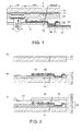
- Fig. 1 is a sectional view for explaining an organic EL display device according to the present invention.
- an organic EL display device 1 is provided by joining a laminate including a thin film circuit layer 20 and an organic EL light emitting layer 30 to a substrate 51 with an adhesive 41 therebetween. Only the substrate 51 is used as the substrate, and this substrate 51 serves both functions of supporting and protecting (sealing) the laminate.
- the adhesive 41 doubles as a protective layer and has moisture resistance and airtightness.
- a substrate insulating film 13 which is a bottom layer of the thin film circuit layer 20 doubles as a protective layer.
- the emitted light from the organic EL light emitting layer radiates in a downward direction in which a so-called element-forming substrate is not present and, therefore, the amount of light is not reduced due to passage through a substrate.
- the connection electrode 18b is exposed at the bottom surface of the thin film circuit layer 20 and the preparation can be performed through one peeling transfer step, as described below. Therefore, the organic EL display device 1 is allowed to become low-profile compared with that in the case where an element-forming substrate and a protective substrate are used and, thereby, a sheet-shaped organic EL display device can be prepared. Any loss due to passage of the emitted light through a substrate is not produced.
- the portion shown in Fig. 1 includes a light emitting element region EL, a thin film transistor (TFT) circuit region TFT, and an external connection region IN/OUT in the organic EL display device 1.
- An organic EL display element emitting the electroluminescent light (EL) is formed from the organic EL layer 30 in the light emitting element region EL.
- a transistor circuit for controlling the action of the organic EL display element is configured by the thin film circuit layer 20 in the thin film transistor circuit region TFT.
- the thin film circuit layer 20 and the organic EL layer 30 are formed from a laminate composed of laminated plural functional layers, e.g., an insulating layer, an electrically conductive layer, a semiconductor layer, a light emitting layer, and an electrode layer.
- connection electrode 18b exposed at the bottom surface of the thin film circuit layer 20 is provided in the external connection region IN/OUT. As described below, the connection electrode 18b is formed to become flush with the bottom surface of a substrate insulating layer.
- the connection electrode 18b is connected to the inside thin film circuit layer 20 and, in addition, is connected to a wiring 62 of an FPC substrate (flexible printed circuit substrate) 61 through an adhesive 72 containing anisotropic conductive materials 71.
- the organic EL display device 1 is supplied with necessary power supply and action signals from the outside through the FPC substrate 61.
- the thin film circuit layer 20 is provided by, for example, film formation of a TFT circuit on the substrate insulating layer 13 composed of a silicon oxide film, silicon nitride film, or other insulating substrate.
- the substrate insulating layer 13 serves a function as a protective layer.
- the substrate insulating layer 13 is composed of one layer, but this may be composed of a plurality of layers.
- the film thickness of the substrate insulating layer 13 is controlled so as not to be in the range of 400 nm to 800 nm and, preferably, at in the order of 300 nm.
- the film thickness of the substrate insulating layer 13 is closely analogous to the wavelength of 400 nm (blue) to 800 nm (red) of the visible light.
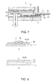
- Fig. 7 shows a comparative example in order to clarify the features of the example.
- the portions corresponding to those in Fig. 1 are indicated by the same reference numerals as in Fig. 1, and explanations thereof will not be provided.
- a thin film circuit layer 20 and an organic EL light emitting layer 30 are provided on an element-forming substrate 11, and a sealing substrate 51 is bonded together with an adhesive 41 therebetween.
- the thin film circuit layer 20 and the organic EL light emitting layer 30 are supported by the element-forming substrate 11 and, in addition, are sealed by the element-forming substrate 11 and the sealing substrate 51, so that permeation of moisture, oxygen, and the like is prevented.
- the perimeter of the substrates are sealed with an adhesive (curable resin), and the connection to an external circuit is performed in the perimeter portion of the substrate 11 through an FPC substrate 61.
- the thickness of the organic EL display device can be reduced.
- the attenuation of the amount of light and the diffuse reflection in the element-forming substrate 11 can be avoided.
- highly flexible materials, e.g. plastic can be used as the substrate 51, the organic EL display device can readily be used for various types of electronic equipment.
- Fig. 8 shows an example of a configuration to extend the life time by preventing permeation of moisture and oxygen into an organic EL display device.
- Fig. 8(a) shows a can sealing type.
- a laminate composed of a thin film circuit layer 20, an organic EL layer 30, and the like provided on an element-forming substrate 11 is sealed by a can package 52 made of a metal, e.g., stainless steel, and a moisture absorbing agent 53, e.g., calcium oxide (CaO), is disposed in the inside.
- a moisture absorbing agent 53 e.g., calcium oxide (CaO)
- the moisture which permeates into the inside is absorbed by the moisture absorbing agent 53 and, thereby, deterioration of a calcium layer 36 in the organic EL layer 30 due to the moisture is prevented.
- Fig. 8(b) shows a substrate sealing type. This type is similar to that shown in Fig. 7. A laminate composed of a thin film circuit layer 20, an organic EL layer 30, and the like is sandwiched between an element-forming substrate 11 and a sealing substrate 51, the perimeters of both the substrates are sealed by a resin 41 and, thereby, permeation of moisture and oxygen into the inside is prevented.
- the configuration of the example of the present invention is superior to any type in points of reduction in film thickness of the organic EL display device and reduction in loss of the light passing through the substrate.
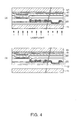
- Fig. 2 to Fig. 5 are process diagrams for explaining a manufacturing process in which an organic EL display device is manufactured by a method for transferring a thin film structure.
- a film of amorphous silicon (a-Si) 12 serving as a release layer is formed from a material gas composed of monosilane (SiH 4 ) by a CVD (chemical vapor deposition) method on a transparent glass substrate 11 which is a first substrate.
- a CVD chemical vapor deposition
- Peeling (may be referred to as "in-layer peeling” or “interfacial peeling”) occurs in the layer or at the interface of the release layer due to application of light, e.g., laser light, as described below. That is, when a certain intensity of light is applied, interatomic or intermolecular binding force disappears or decreases with respect to atoms and molecules constituting the constituents, and ablation and the like occur so as to cause peeling.
- the application of the light may cause release of gases from the release layer and, thereby, separation may occur.
- Amorphous silicon (a-Si) is suitable as a component of such a release layer, although not limited to this.
- This amorphous silicon may contain hydrogen.
- the content of hydrogen is at least about 2 atomic percent, and more preferably is 2 to 20 atomic percent.
- hydrogen is released by application of the light and, thereby, an internal pressure is generated in the release layer so as to accelerate the peeling.
- the content of hydrogen is adjusted by the film formation condition. For example, in the case where a CVD method is used, conditions, e.g., a gas composition, a gas pressure, a gas atmosphere, a gas flow rate, a gas temperature, a substrate temperature, and a power of the light input, are appropriately controlled.
- a thin film circuit layer including a thin film transistor (TFT), an electrode, and the like is formed.
- a silicon dioxide layer (SiO 2 ) 13 serving as a substrate insulating layer having a film thickness in the order of 300 nm is formed from material gases composed of monosilane (SiH 4 ) and oxygen (O 2 ) by a CVD method on the above-described amorphous silicon 12.
- a silicon layer 14 serving as a semiconductor layer is formed on the silicon dioxide layer 13 serving as a under layer.
- the silicon layer 14 can be formed from a material gas composed of monosilane (SiH 4 ) by a CVD method.
- the resulting silicon layer 14 is subjected to a heat treatment with an excimer laser or the like and, thereby, is allowed to polycrystallize.
- a polycrystalline silicon layer may be formed by a plasma CVD merhod.
- the resulting polycrystalline silicon layer 14 is patterned by a photoetching method so as to form an active region in which a thin film transistor is formed.
- a silicon dioxide layer 15 serving as a gate insulating film is formed on the resulting silicon layer 14 by, for example, a thermal oxidation method or a PECVD method through the use of TEOS or the like as a material.
- a polycrystalline silicon layer containing a high concentration of impurities is formed thereon by the CVD method, and is patterned by the photoetching method so as to form a gate electrode and wiring 16.
- a metal thin film primarily containing aluminum, chromium, molybdenum, tantalum, or the like is formed by sputtering, and this is patterned, so that the gate electrode and wiring 16 can also be formed.
- Impurities for example, phosphorus ions
- Impurities are implanted at a high concentration into a source-drain region of an N-type thin film transistor by an ion plantation method through the use of a resist, although not shown in the drawing, and the gate electrode 16 as masks.
- impurities for example, boron ions
- a silicon dioxide layer 17 is formed from material gases composed of monosilane (SiH 4 ) and oxygen (O 2 ) by the CVD method on the gate insulating film 15 and the gate electrode and wiring 16 so as to form an interlayer insulation film.
- a contact hole is opened in the silicon oxide film 17 on the source-drain region of the thin film transistor by the photoetching method.
- the region to be provided with a connection electrode is subjected to etching until the amorphous silicon layer 12 is exposed.
- a metal layer of aluminum or the like or a polycrystalline silicon layer doped with impurities is formed as a source-drain electrode, a wiring, and a connection electrode. Patterning is performed by the photoetching method and, thereby, a source-drain electrode and wiring 18 is formed.
- a silicon dioxide layer 19 is formed from material gases composed of monosilane (SiH 4 ) and oxygen (O 2 ) by the CVD method on the source-drain electrode and wiring 18 and the like so as to form a protective layer.
- the surface of the resulting protective layer 19 is flattened by polishing.
- the silicon dioxide layer 19 on the drain electrode is partially provided with an opening by the photoetching method.
- a transparent electrode layer made of ITO or the like is formed thereon, and is patterned by the photoetching method so as to form a lower electrode layer 31 of an organic EL light emitting element.
- a silicon dioxide layer 32 is formed thereon by the CVD method, and is provided with an opening at the portion corresponding to the lower electrode (ITO) 31 by the photoetching method. Furthermore, a photosensitive resin 33 is applied as a bank layer to separate pixel regions, and patterning exposure is performed to provide an opening at the portion corresponding to the lower electrode 31, followed by development, so as to provide an opening above the lower electrode 31. The photosensitive resin 33 in a cured state is used as a bank film material.
- the thin film circuit layer 20 is composed of layers from the substrate insulating layer 13 to the protective layer 19.
- an organic EL material is discharged from, for example, a droplet discharge head, not shown in the drawing, on the lower electrode 31, so as to form a coating film, and, thereby, a light emitting layer is provided.
- a material for films of a hole transporting layer 34 and an EL light emitting layer 35 serving as light emitting layers is applied on the lower electrode 31 with the droplet discharge head so as to form films.
- a calcium layer 36 is formed thereon as an electron transporting layer.
- An aluminum layer 37 serving as a cathode is formed on the calcium layer 36 by a sputtering method, a vacuum evaporation method, or the like.
- a silicon nitride layer (Si x N y ) 38 is formed thereon from material gases composed of monosilane (SiH 4 ) and ammonia (NH 3 ) by the CVD method in order to prevent permeation of gases and moisture into the calcium layer 36 and, therefore, a protective layer 38 is provided (Fig. 3(b)).
- the organic EL light emitting layer 30 is composed of layers from the lower electrode layer 31 to the protective layer 38.
- a plastic substrate for example, can be used as the substrate 51.
- a water-resistant, gas-resistant curable resin is used as the adhesive 41, so that moisture and oxygen hardly pass through the adhesive 41.
- the substrate 51 and the adhesive 41 serve functions as a sealing substrate and a sealing agent, respectively.
- the substrate 11 is peeled off.
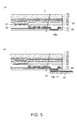
- the amorphous silicon layer 12 serving as a release layer is irradiated with an excimer laser from the back side of the transparent substrate 11 so as to cause ablation or to vaporize and expand vaporizable components and, thereby, peeling is allowed to occur in the amorphous silicon layer 12 (in-layer peeling) or at the interface to the substrate 11 or at the interface to the substrate insulating layer 13 (interfacial peeling) (Fig. 4(a)).
- the glass substrate 11 is peeled off along the release layer 12, and is separated. In this manner, the thin film circuit layer 30 is transferred (shifted) from the glass substrate 11 side to the temporary transfer substrate 33 side (Fig. 4(b)).
- the substrate 11 may be removed by dissolution with, for example, a solution containing hydrofluoric acid, in place of the above-described step.
- a solution containing hydrofluoric acid for example, a solution containing hydrofluoric acid
- the etching rate of the amorphous silicon layer 12, which is a constituent material of the release layer is adequately small and, therefore, the advance of corrosion can be stopped after the substrate 11 is removed, while the release layer 12 is in the state of being exposed. Consequently, only the substrate 11 can be removed by dissolution while the TFT circuit layer is not eroded by the etching solution.
- the remaining release layer 12 left at the bottom portion of the thin film circuit layer 20 is removed by etching, so that a face-down type organic EL display device 1 which radiates the emitted light downward is formed (Fig. 5(a)).
- connection electrode 18b exposed at the bottom surface of the resulting organic EL display device 1 and a wiring 62 of an FPC substrate 61 connected to an external driving circuit and the like, although not shown in the drawing, are connected with an adhesive 72 through anisotropic conductive materials 71.
- the anisotropic conductive materials 71 have a property of conducting in the direction of compression. In this manner, the organic EL display device 1 is connected to external circuits, e.g., an image display circuit (Fig. 5(b)).
- the target for the transfer is the laminate constituting the organic EL display device 1.
- the microstructure targeted for the transfer can be formed alone or together with the thin film circuit layer at this portion.
- microstructures include piezoelectric vibrators, electrostatic vibrators, actuators, diffraction gratings, micromirrors, microlenses, optical elements, probe structures of living body specimens and DNA specimens, and the like.
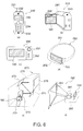
- Fig. 6 shows examples of electronic equipment including an organic EL display device which is an electro-optic device.
- Fig. 6(a) shows an example of application to a cellular phone.
- a cellular phone 230 is provided with an antenna portion 231, a voice output portion 232, a voice input portion 233, a control portion 234, and an organic EL display device 100.
- the organic EL display device of the present invention can be used as a display portion of the cellular phone 230.
- Fig. 6(b) shows an example of application to a video camera.
- a video camera 240 is provided with an image receiving portion 241, a control portion 242, a voice input portion 243, and an organic EL display device 100.
- the organic EL display device of the present invention can be used as a finder and a display portion.
- Fig. 6(c) shows an example of application to a portable personal computer.
- a computer 250 is provided with a camera portion 251, a control portion 252, and an organic EL display device 100.
- the organic EL display device of the present invention can be used as a display portion.
- Fig. 6(d) shows an example of application to a head mount display.
- a head mount display 260 is provided with a band 261, an optical system storage portion 262, and an organic EL display device 100.
- the organic EL display device of the present invention can be used as an image display.
- Fig. 6(e) shows an example of application to a rear type projector.
- a projector 270 is provided with a light source 272, a synthetic optical system 273, a mirror 274, a mirror 275, a screen 276, and an organic EL display device 100 in a cabinet 271. In this manner, the organic EL display device of the present invention can be used as an image display.
- FIG. 6(f) shows an example of application to a front type projector.
- a projector 280 is provided with an optical system 281 and an organic EL display device 100 in a cabinet 282, and an image can be displayed on a screen 283.
- the organic EL display device of the present invention can be used as an image display.
- the organic EL display device of the present invention can be applied to various electronic equipment, not limited to the above-described examples.
- the organic EL display device can also be used for facsimiles with a display function, finders of digital cameras, portable TVs, DSP devices, PDAs, electronic notepads, electric bulletin boards, advertisement displays, and the like.
- the organic EL display device (or the display panel) is formed on one substrate and, therefore, a low-profile display device can be provided. Furthermore, the light is emitted from the side opposite to the substrate and, therefore, any loss due to the substrate can be avoided.
- Such an organic EL display device can be prepared through one pass of peeling transfer by the use of the peeling transfer method.
- the above-described one substrate may be a plastic substrate.
Landscapes
- Engineering & Computer Science (AREA)
- Manufacturing & Machinery (AREA)
- Microelectronics & Electronic Packaging (AREA)
- Electroluminescent Light Sources (AREA)
Abstract
Description
- The present invention relates to an improvement of an organic EL display device. In particular, it relates to an organic EL display device which can be prepared with a reduced thickness, electronic equipment including the same, and a method for manufacturing the same.
- With respect to semiconductor devices and the like, a high-temperature treatment step and the like are included in the process of manufacturing laminates composed of required microstructures, thin film circuits, and the like on substrates and, therefore, selection of elements constituting substrates and laminates may be restricted. For example, resin films, plastic substrates, and the like are not suitable for a high-temperature treatment.
- Consequently, for example, in the invention described in Japanese Unexamined Patent Application Publication No. 2002-217391, a thin film circuit is formed on a heat-resistant element-forming substrate with a first release layer therebetween, a temporary transfer substrate is adhered to this thin film circuit with a second release layer therebetween, and the first release layer is broken, so that the thin film circuit is transferred from the element-forming substrate side to the temporary transfer substrate side. Furthermore, a final substrate is bonded together with the temporary transfer substrate and, thereafter, the second release layer is broken, so that the thin film circuit is transferred from the temporary transfer substrate side to the final substrate side. In this manner, the thin film circuit is disposed on a plastic substrate through film formation steps in the order similar to that in the case where the thin film circuit is formed on the element-forming substrate. Here, the thin film circuit includes a thin film transistor (TFT) circuit, a TFT circuit substrate of a liquid crystal display, an organic EL display device, and the like.
- However, when the organic EL display device is transferred to the final substrate by repeating the peeling transfer between substrates as many as two times, as described above, the number of manufacturing steps is increased, and the manufacturing process becomes complicated.
- An organic EL display device can be formed on a highly flexible plastic thin film substrate by the use of the above-described peeling transfer technology. Accordingly, it is expected that a sheet-shaped thin organic EL display panel will be provided. However, in order to prevent permeation of moisture and oxygen into light emitting elements, the organic EL display device is required to include a sealing substrate for covering and protecting a group of light emitting elements, besides the above-described plastic substrate. Consequently, even when a thin plastic substrate is used, there is a certain limit to reduction in the total thickness of the display panel. Furthermore, the light radiated from an organic EL light emitting element located between the two substrates is emitted to the outside through one of the substrate and, thereby, a transmission loss is produced during passage through the substrate.
- Accordingly, it is an object of the present invention to provide an organic EL display device in which a transmission loss due to a substrate is reduced.
- It is also an object of the present invention to provide a sheet-shaped organic EL display device having a reduced thickness.
- It is also an object of the present invention to provide electronic equipment including the above-described organic EL display device.
- It is also an object of the present invention to provide a method for manufacturing the above-described organic EL display device.
- In order to achieve the above-described objects, an organic EL display device of the present invention includes a substrate serving as both a protective layer to prevent permeation of moisture, oxygen, and the like into the inside and a support layer for film formation; a laminate which is provided on a under layer by film formation and which includes a thin film circuit layer carrying an electric circuit and an organic EL light emitting layer carrying an organic EL light emitting element to radiate the emitted light toward the above-described under layer side; and an adhesive layer joining the above-described laminate and the above-described substrate, and the above-described organic EL light emitting element radiates the emitted light toward the above-described under layer side.
- By adopting such a configuration, a low-profile organic EL display device including one substrate can be provided. Since the organic EL light can radiate to the outside not through the substrate, the loss of the amount of light due to passage through the substrate and multiple reflection at the substrate can be avoided. Furthermore, the substrate, the adhesive layer, and the under layer form protective layers and, thereby, the permeation of moisture and oxygen into the inside of the device can be suppressed.
- Preferably, a connection electrode is included, which penetrates a part of the above-described under layer so as to be exposed at the bottom surface of the under layer and which connects an external circuit and the above-described electric circuit. In this manner, the connection to the external circuit can be readily performed. Furthermore, a connection terminal can be ensured by even one time of peeling transfer.
- Preferably, the film thickness of the above-described under layer is not in the range of 400 (blue) to 800 (red) nm. More preferably, the thickness is controlled at 300 nm or less. In this manner, occurrence of interference can be avoided when the emitted light (visible light) passes through the under layer.
- Preferably, the above-described substrate is a plastic substrate. In this manner, a sheet-shaped display device resistant to bending and shock is readily provided. However, a glass substrate may be adopted.
- Preferably, the mutual connection between the above-described connection electrode and the above-described external circuit is performed through anisotropic conductive materials or an electrically conductive adhesive. In this manner, the connection to the external circuit can be readily performed.
- Preferably, the above-described connection electrode is formed to become substantially flush with the above-described under layer. In this manner, the handling and the wiring connection can readily be performed in the following steps.
- Electronic equipment of the present invention includes the above-described organic EL display device and, therefore, the display portion can readily be configured to become low-profile. The electronic equipment is, for example, the equipment including the organic EL display device as a display portion, and examples thereof include video cameras, televisions, large screens, cellular phones, personal computers, personal digital assistants (so-called PDAs), and the like.
- A method for manufacturing an organic EL display device of the present invention includes the steps of forming a release layer on a first substrate; forming a laminate on the above-described release layer, the laminate including an organic EL light emitting layer which emits light toward the release layer side; joining the above-described first substrate provided with the above-described laminate and a second substrate with an adhesive layer therebetween; and applying energy to the above-described release layer so as to cause peeling, and peeling off the above-described first substrate so as to transfer the above-described laminate to the above-described second substrate side.
- A method for manufacturing an organic EL display device according to another aspect of the present invention includes the steps of forming a release layer on a first substrate; forming a laminate on the above-described release layer, the laminate including an organic EL light emitting layer which emits light toward the release layer side; joining the first substrate provided with the above-described laminate and a second substrate with an adhesive layer therebetween; and removing the above-described first substrate by dissolution so as to transfer the above-described laminate to the above-described second substrate side.
- By adopting such a configuration, an organic EL display device having the above-described features can be formed.
- Preferably, the step of forming a connection electrode exposed at a part of the bottom surface of the above-described laminate is further included. In this manner, the connection to an external circuit is readily performed.
- Embodiments of the present invention will now be described by way of further example only and with reference to the accompanying drawings, in which:
- Fig. 1 is a sectional view for explaining an example of an organic EL display device of the present invention.
- Fig. 2(a) to Fig. 2(c) are process diagrams for explaining a manufacturing , process of an organic EL display device in an example.
- Fig. 3(a) to Fig. 3(c) are process diagrams for explaining the manufacturing process of the organic EL display device in the example.
- Fig. 4(a) and Fig. 4(b) are process diagrams for explaining the manufacturing process of the organic EL display device in the example.
- Fig. 5(a) and Fig. 5(b) are process diagrams for explaining the manufacturing process of the organic EL display device in the example.
- Fig. 6 is a diagram for explaining examples of electronic equipment including an organic EL display device.
- Fig. 7 is a sectional view for explaining an organic EL display device in a comparative example.
- Fig. 8(a) and Fig. 8(b) are diagrams for explaining sealing types of an organic EL display device.
-
- An organic EL display device according to the example has a configuration in which a substrate provided to support a laminate including a TFT circuit layer, an organic EL light emitting layer, and the like doubles as a sealing substrate and, thereby, one of two substrates of an element-forming substrate and a sealing substrate is unnecessary. Consequently. the laminate is formed in order that a connection electrode is exposed at the back side, the resulting laminate is transferred to a final substrate through one transfer described below, and the final substrate is used as a support substrate for the laminate and the sealing substrate. The light emitted from the organic EL light emitting layer is output toward the back side of the laminate while a glass substrate and the like do not intervene. The external circuit is connected to the back side of the laminate through the use of the connection electrode.
- Fig. 1 is a sectional view for explaining an organic EL display device according to the present invention.
- As shown in Fig. 1, an organic
EL display device 1 is provided by joining a laminate including a thinfilm circuit layer 20 and an organic ELlight emitting layer 30 to asubstrate 51 with an adhesive 41 therebetween. Only thesubstrate 51 is used as the substrate, and thissubstrate 51 serves both functions of supporting and protecting (sealing) the laminate. Theadhesive 41 doubles as a protective layer and has moisture resistance and airtightness. In addition, asubstrate insulating film 13 which is a bottom layer of the thinfilm circuit layer 20 doubles as a protective layer. - According to this configuration, the emitted light from the organic EL light emitting layer radiates in a downward direction in which a so-called element-forming substrate is not present and, therefore, the amount of light is not reduced due to passage through a substrate. The
connection electrode 18b is exposed at the bottom surface of the thinfilm circuit layer 20 and the preparation can be performed through one peeling transfer step, as described below. Therefore, the organicEL display device 1 is allowed to become low-profile compared with that in the case where an element-forming substrate and a protective substrate are used and, thereby, a sheet-shaped organic EL display device can be prepared. Any loss due to passage of the emitted light through a substrate is not produced. - The portion shown in Fig. 1 includes a light emitting element region EL, a thin film transistor (TFT) circuit region TFT, and an external connection region IN/OUT in the organic
EL display device 1. An organic EL display element emitting the electroluminescent light (EL) is formed from theorganic EL layer 30 in the light emitting element region EL. A transistor circuit for controlling the action of the organic EL display element is configured by the thinfilm circuit layer 20 in the thin film transistor circuit region TFT. The thinfilm circuit layer 20 and theorganic EL layer 30 are formed from a laminate composed of laminated plural functional layers, e.g., an insulating layer, an electrically conductive layer, a semiconductor layer, a light emitting layer, and an electrode layer. Theconnection electrode 18b exposed at the bottom surface of the thinfilm circuit layer 20 is provided in the external connection region IN/OUT. As described below, theconnection electrode 18b is formed to become flush with the bottom surface of a substrate insulating layer. Theconnection electrode 18b is connected to the inside thinfilm circuit layer 20 and, in addition, is connected to awiring 62 of an FPC substrate (flexible printed circuit substrate) 61 through an adhesive 72 containing anisotropicconductive materials 71. The organicEL display device 1 is supplied with necessary power supply and action signals from the outside through theFPC substrate 61. - The thin
film circuit layer 20 is provided by, for example, film formation of a TFT circuit on thesubstrate insulating layer 13 composed of a silicon oxide film, silicon nitride film, or other insulating substrate. Thesubstrate insulating layer 13 serves a function as a protective layer. In the example shown in the drawing, thesubstrate insulating layer 13 is composed of one layer, but this may be composed of a plurality of layers. The film thickness of thesubstrate insulating layer 13 is controlled so as not to be in the range of 400 nm to 800 nm and, preferably, at in the order of 300 nm. Consequently, when the emitted light (visible light) from the organic EL light emitting element passes through thesubstrate insulating layer 13, occurrence of interference in the substrate insulating layer is avoided because the film thickness of thesubstrate insulating layer 13 is closely analogous to the wavelength of 400 nm (blue) to 800 nm (red) of the visible light. - Fig. 7 shows a comparative example in order to clarify the features of the example. In Fig. 7, the portions corresponding to those in Fig. 1 are indicated by the same reference numerals as in Fig. 1, and explanations thereof will not be provided.
- In the configuration of the comparative example, a thin
film circuit layer 20 and an organic ELlight emitting layer 30 are provided on an element-formingsubstrate 11, and a sealingsubstrate 51 is bonded together with an adhesive 41 therebetween. The thinfilm circuit layer 20 and the organic ELlight emitting layer 30 are supported by the element-formingsubstrate 11 and, in addition, are sealed by the element-formingsubstrate 11 and the sealingsubstrate 51, so that permeation of moisture, oxygen, and the like is prevented. The perimeter of the substrates are sealed with an adhesive (curable resin), and the connection to an external circuit is performed in the perimeter portion of thesubstrate 11 through anFPC substrate 61. - As is clear from comparison with the comparative example, since the element-forming
substrate 11 is not used in the configuration of the present example shown in Fig. 1, the thickness of the organic EL display device can be reduced. The attenuation of the amount of light and the diffuse reflection in the element-formingsubstrate 11 can be avoided.
Since highly flexible materials, e.g. plastic, can be used as thesubstrate 51, the organic EL display device can readily be used for various types of electronic equipment. - Fig. 8 shows an example of a configuration to extend the life time by preventing permeation of moisture and oxygen into an organic EL display device.
- Fig. 8(a) shows a can sealing type. In this type, a laminate composed of a thin
film circuit layer 20, anorganic EL layer 30, and the like provided on an element-formingsubstrate 11 is sealed by a can package 52 made of a metal, e.g., stainless steel, and amoisture absorbing agent 53, e.g., calcium oxide (CaO), is disposed in the inside. The moisture which permeates into the inside is absorbed by themoisture absorbing agent 53 and, thereby, deterioration of acalcium layer 36 in theorganic EL layer 30 due to the moisture is prevented. - Fig. 8(b) shows a substrate sealing type. This type is similar to that shown in Fig. 7. A laminate composed of a thin
film circuit layer 20, anorganic EL layer 30, and the like is sandwiched between an element-formingsubstrate 11 and a sealingsubstrate 51, the perimeters of both the substrates are sealed by aresin 41 and, thereby, permeation of moisture and oxygen into the inside is prevented. - The configuration of the example of the present invention is superior to any type in points of reduction in film thickness of the organic EL display device and reduction in loss of the light passing through the substrate.
- Fig. 2 to Fig. 5 are process diagrams for explaining a manufacturing process in which an organic EL display device is manufactured by a method for transferring a thin film structure.
- As shown in Fig. 2(a), a film of amorphous silicon (a-Si) 12 serving as a release layer is formed from a material gas composed of monosilane (SiH4) by a CVD (chemical vapor deposition) method on a
transparent glass substrate 11 which is a first substrate. - Peeling (may be referred to as "in-layer peeling" or "interfacial peeling") occurs in the layer or at the interface of the release layer due to application of light, e.g., laser light, as described below. That is, when a certain intensity of light is applied, interatomic or intermolecular binding force disappears or decreases with respect to atoms and molecules constituting the constituents, and ablation and the like occur so as to cause peeling. The application of the light may cause release of gases from the release layer and, thereby, separation may occur. There are a case where components contained in the release layer are vaporized and released so as to cause the separation and a case where the release layer is vaporized due to absorption of the light, and the resulting vapors are released so as to cause the separation. Amorphous silicon (a-Si) is suitable as a component of such a release layer, although not limited to this.
- This amorphous silicon may contain hydrogen. Preferably, the content of hydrogen is at least about 2 atomic percent, and more preferably is 2 to 20 atomic percent. When hydrogen is contained, hydrogen is released by application of the light and, thereby, an internal pressure is generated in the release layer so as to accelerate the peeling. The content of hydrogen is adjusted by the film formation condition. For example, in the case where a CVD method is used, conditions, e.g., a gas composition, a gas pressure, a gas atmosphere, a gas flow rate, a gas temperature, a substrate temperature, and a power of the light input, are appropriately controlled. Next, as shown in Fig. 2(b), a thin film circuit layer including a thin film transistor (TFT), an electrode, and the like is formed. A silicon dioxide layer (SiO2) 13 serving as a substrate insulating layer having a film thickness in the order of 300 nm is formed from material gases composed of monosilane (SiH4) and oxygen (O2) by a CVD method on the above-described
amorphous silicon 12. Asilicon layer 14 serving as a semiconductor layer is formed on thesilicon dioxide layer 13 serving as a under layer. Thesilicon layer 14 can be formed from a material gas composed of monosilane (SiH4) by a CVD method. The resultingsilicon layer 14 is subjected to a heat treatment with an excimer laser or the like and, thereby, is allowed to polycrystallize. A polycrystalline silicon layer may be formed by a plasma CVD merhod. The resultingpolycrystalline silicon layer 14 is patterned by a photoetching method so as to form an active region in which a thin film transistor is formed. - A
silicon dioxide layer 15 serving as a gate insulating film is formed on the resultingsilicon layer 14 by, for example, a thermal oxidation method or a PECVD method through the use of TEOS or the like as a material. A polycrystalline silicon layer containing a high concentration of impurities is formed thereon by the CVD method, and is patterned by the photoetching method so as to form a gate electrode andwiring 16. Alternatively, a metal thin film primarily containing aluminum, chromium, molybdenum, tantalum, or the like is formed by sputtering, and this is patterned, so that the gate electrode andwiring 16 can also be formed. - Impurities (for example, phosphorus ions) are implanted at a high concentration into a source-drain region of an N-type thin film transistor by an ion plantation method through the use of a resist, although not shown in the drawing, and the
gate electrode 16 as masks. Likewise, impurities (for example, boron ions) are implanted at a high concentration into a source-drain region of a P-type thin film transistor by an ion plantation method through the use of the resist and thegate electrode 16 as masks. Thereafter, a heat treatment is performed, so that the impurities are activated. Asilicon dioxide layer 17 is formed from material gases composed of monosilane (SiH4) and oxygen (O2) by the CVD method on thegate insulating film 15 and the gate electrode andwiring 16 so as to form an interlayer insulation film. - A contact hole is opened in the
silicon oxide film 17 on the source-drain region of the thin film transistor by the photoetching method. The region to be provided with a connection electrode is subjected to etching until theamorphous silicon layer 12 is exposed. A metal layer of aluminum or the like or a polycrystalline silicon layer doped with impurities is formed as a source-drain electrode, a wiring, and a connection electrode. Patterning is performed by the photoetching method and, thereby, a source-drain electrode andwiring 18 is formed. - As shown in Fig. 2(c), a
silicon dioxide layer 19 is formed from material gases composed of monosilane (SiH4) and oxygen (O2) by the CVD method on the source-drain electrode andwiring 18 and the like so as to form a protective layer. The surface of the resultingprotective layer 19 is flattened by polishing. Thesilicon dioxide layer 19 on the drain electrode is partially provided with an opening by the photoetching method. A transparent electrode layer made of ITO or the like is formed thereon, and is patterned by the photoetching method so as to form alower electrode layer 31 of an organic EL light emitting element. Asilicon dioxide layer 32 is formed thereon by the CVD method, and is provided with an opening at the portion corresponding to the lower electrode (ITO) 31 by the photoetching method. Furthermore, aphotosensitive resin 33 is applied as a bank layer to separate pixel regions, and patterning exposure is performed to provide an opening at the portion corresponding to thelower electrode 31, followed by development, so as to provide an opening above thelower electrode 31. Thephotosensitive resin 33 in a cured state is used as a bank film material. The thinfilm circuit layer 20 is composed of layers from thesubstrate insulating layer 13 to theprotective layer 19. - As shown in Fig. 3(a), an organic EL material is discharged from, for example, a droplet discharge head, not shown in the drawing, on the
lower electrode 31, so as to form a coating film, and, thereby, a light emitting layer is provided. For example, a material for films of ahole transporting layer 34 and an ELlight emitting layer 35 serving as light emitting layers is applied on thelower electrode 31 with the droplet discharge head so as to form films. Acalcium layer 36, for example, is formed thereon as an electron transporting layer. - An
aluminum layer 37 serving as a cathode is formed on thecalcium layer 36 by a sputtering method, a vacuum evaporation method, or the like. A silicon nitride layer (SixNy) 38 is formed thereon from material gases composed of monosilane (SiH4) and ammonia (NH3) by the CVD method in order to prevent permeation of gases and moisture into thecalcium layer 36 and, therefore, aprotective layer 38 is provided (Fig. 3(b)). The organic ELlight emitting layer 30 is composed of layers from thelower electrode layer 31 to theprotective layer 38. - The
substrate 11 provided with the thin film circuits, e.g., the TFT circuit layer and the light emitting layer, is bonded together with asubstrate 51 through an adhesive 41 (Fig. 3(c)). A plastic substrate, for example, can be used as thesubstrate 51. A water-resistant, gas-resistant curable resin is used as the adhesive 41, so that moisture and oxygen hardly pass through the adhesive 41. Thesubstrate 51 and the adhesive 41 serve functions as a sealing substrate and a sealing agent, respectively. - As shown in Fig. 4, the
substrate 11 is peeled off. Theamorphous silicon layer 12 serving as a release layer is irradiated with an excimer laser from the back side of thetransparent substrate 11 so as to cause ablation or to vaporize and expand vaporizable components and, thereby, peeling is allowed to occur in the amorphous silicon layer 12 (in-layer peeling) or at the interface to thesubstrate 11 or at the interface to the substrate insulating layer 13 (interfacial peeling) (Fig. 4(a)). - The
glass substrate 11 is peeled off along therelease layer 12, and is separated. In this manner, the thinfilm circuit layer 30 is transferred (shifted) from theglass substrate 11 side to thetemporary transfer substrate 33 side (Fig. 4(b)). - The
substrate 11 may be removed by dissolution with, for example, a solution containing hydrofluoric acid, in place of the above-described step. At that time, when an aqueous solution of hydrofluoric acid is used, the etching rate of theamorphous silicon layer 12, which is a constituent material of the release layer, is adequately small and, therefore, the advance of corrosion can be stopped after thesubstrate 11 is removed, while therelease layer 12 is in the state of being exposed. Consequently, only thesubstrate 11 can be removed by dissolution while the TFT circuit layer is not eroded by the etching solution. - As shown in Fig. 5, the remaining
release layer 12 left at the bottom portion of the thinfilm circuit layer 20 is removed by etching, so that a face-down type organicEL display device 1 which radiates the emitted light downward is formed (Fig. 5(a)). - The
connection electrode 18b exposed at the bottom surface of the resulting organicEL display device 1 and awiring 62 of anFPC substrate 61 connected to an external driving circuit and the like, although not shown in the drawing, are connected with an adhesive 72 through anisotropicconductive materials 71. The anisotropicconductive materials 71 have a property of conducting in the direction of compression. In this manner, the organicEL display device 1 is connected to external circuits, e.g., an image display circuit (Fig. 5(b)). - In the present example, the target for the transfer is the laminate constituting the organic
EL display device 1. However, in other thin film devices, the microstructure targeted for the transfer can be formed alone or together with the thin film circuit layer at this portion. As described above, microstructures include piezoelectric vibrators, electrostatic vibrators, actuators, diffraction gratings, micromirrors, microlenses, optical elements, probe structures of living body specimens and DNA specimens, and the like. - Fig. 6 shows examples of electronic equipment including an organic EL display device which is an electro-optic device. Fig. 6(a) shows an example of application to a cellular phone. A
cellular phone 230 is provided with anantenna portion 231, avoice output portion 232, avoice input portion 233, acontrol portion 234, and an organicEL display device 100. In this manner, the organic EL display device of the present invention can be used as a display portion of thecellular phone 230. Fig. 6(b) shows an example of application to a video camera. Avideo camera 240 is provided with animage receiving portion 241, acontrol portion 242, avoice input portion 243, and an organicEL display device 100. In this manner, the organic EL display device of the present invention can be used as a finder and a display portion. Fig. 6(c) shows an example of application to a portable personal computer. Acomputer 250 is provided with acamera portion 251, acontrol portion 252, and an organicEL display device 100. In this manner, the organic EL display device of the present invention can be used as a display portion. - Fig. 6(d) shows an example of application to a head mount display. A
head mount display 260 is provided with aband 261, an opticalsystem storage portion 262, and an organicEL display device 100. In this manner, the organic EL display device of the present invention can be used as an image display. Fig. 6(e) shows an example of application to a rear type projector. Aprojector 270 is provided with alight source 272, a syntheticoptical system 273, amirror 274, amirror 275, ascreen 276, and an organicEL display device 100 in acabinet 271. In this manner, the organic EL display device of the present invention can be used as an image display. - Fig. 6(f) shows an example of application to a front type projector. A
projector 280 is provided with anoptical system 281 and an organicEL display device 100 in acabinet 282, and an image can be displayed on ascreen 283. In this manner, the organic EL display device of the present invention can be used as an image display. - The organic EL display device of the present invention can be applied to various electronic equipment, not limited to the above-described examples. For example, the organic EL display device can also be used for facsimiles with a display function, finders of digital cameras, portable TVs, DSP devices, PDAs, electronic notepads, electric bulletin boards, advertisement displays, and the like.
- As described above, according to the present invention, the organic EL display device (or the display panel) is formed on one substrate and, therefore, a low-profile display device can be provided. Furthermore, the light is emitted from the side opposite to the substrate and, therefore, any loss due to the substrate can be avoided. Such an organic EL display device can be prepared through one pass of peeling transfer by the use of the peeling transfer method. According to the peeling transfer method, the above-described one substrate may be a plastic substrate.
Claims (6)
- An organic EL display device, comprising:a substrate serving as both a seal to reduce or prevent permeation of gas into an inside of the display device and a support for film formation;a laminate provided on an under layer of the substrate by film formation and includes a thin film circuit layer carrying an electric circuit and an organic EL light emitting layer carrying an organic EL light emitting element to radiate emitted light toward the under layer; andan adhesive layer joining the laminate and the substrate.
- The organic EL display device according to Claim 1, further comprising:a connection electrode which penetrates a part of the under layer so as to be exposed at the bottom surface of the under layer and which connects an external circuit and the electric circuit.
- The organic EL display device according to Claim 1 or 2, wherein the film thickness of the under layer being not in the range of 400 to 800 nm.
- Electronic equipment , comprising:the organic EL display device according to any one of Claims 1 to 3 as a display portion.
- A method to manufacture an organic EL display device, comprising:forming a release layer on a first substrate;forming a laminate on the release layer, the laminate including an organic EL light emitting layer which emits light toward the release layer side;joining the first substrate provided with the laminate and a second substrate with an adhesive layer therebetween; andapplying energy to the release layer so as to cause peeling, and peeling off the first substrate so as to transfer the laminate to the second substrate side.
- A method for manufacturing an organic EL display device, comprising:forming a release layer on a first substrate;forming a laminate on the release layer, the laminate including an organic EL light emitting layer which emits light toward the release layer side;joining the first substrate provided with the laminate and a second substrate with an adhesive layer therebetween; andremoving the first substrate by dissolution so as to transfer the laminate to the second substrate side.
Applications Claiming Priority (2)
| Application Number | Priority Date | Filing Date | Title |
|---|---|---|---|
| JP2003146142 | 2003-05-23 | ||
| JP2003146142A JP3897173B2 (en) | 2003-05-23 | 2003-05-23 | Organic EL display device and manufacturing method thereof |
Publications (2)
| Publication Number | Publication Date |
|---|---|
| EP1480272A2 true EP1480272A2 (en) | 2004-11-24 |
| EP1480272A3 EP1480272A3 (en) | 2005-10-26 |
Family
ID=33095484
Family Applications (1)
| Application Number | Title | Priority Date | Filing Date |
|---|---|---|---|
| EP04253023A Withdrawn EP1480272A3 (en) | 2003-05-23 | 2004-05-21 | Organic EL display device, electronic equipment, and method for manufacturing the same |
Country Status (6)
| Country | Link |
|---|---|
| US (1) | US7342354B2 (en) |
| EP (1) | EP1480272A3 (en) |
| JP (1) | JP3897173B2 (en) |
| KR (1) | KR100627097B1 (en) |
| CN (1) | CN100446268C (en) |
| TW (1) | TWI255151B (en) |
Cited By (6)
| Publication number | Priority date | Publication date | Assignee | Title |
|---|---|---|---|---|
| WO2008003166A1 (en) * | 2006-07-05 | 2008-01-10 | Ifire Ip Corporation | Sealed thick film dielectric electroluminescent display |
| US8222666B2 (en) | 2008-12-17 | 2012-07-17 | Semiconductor Energy Laboratory Co., Ltd. | Light-emitting device and electronic device |
| WO2019115518A1 (en) * | 2017-12-12 | 2019-06-20 | Fraunhofer-Gesellschaft zur Förderung der angewandten Forschung e. V. | Method for producing a semi-transparent display and a semi-transparent display |
| US10496203B2 (en) | 2014-04-25 | 2019-12-03 | Semiconductor Energy Laboratory Co., Ltd. | Display device and electronic device |
| US11054687B2 (en) | 2016-08-09 | 2021-07-06 | Semiconductor Energy Laboratory Co., Ltd. | Method for manufacturing display device, display device, display module, and electronic device |
| US12389677B2 (en) | 2013-03-14 | 2025-08-12 | Semiconductor Energy Laboratory Co., Ltd. | Light-emitting device and method for manufacturing the same |
Families Citing this family (39)
| Publication number | Priority date | Publication date | Assignee | Title |
|---|---|---|---|---|
| JP5202673B2 (en) * | 2001-07-27 | 2013-06-05 | 株式会社半導体エネルギー研究所 | Method for manufacturing semiconductor device |
| JP2007184251A (en) * | 2005-12-07 | 2007-07-19 | Sony Corp | Display device |
| JP2008021629A (en) * | 2006-07-11 | 2008-01-31 | Samsung Sdi Co Ltd | Organic electroluminescence display |
| JP5368013B2 (en) * | 2008-06-24 | 2013-12-18 | 共同印刷株式会社 | Manufacturing method of flexible organic EL display |
| JP5368014B2 (en) * | 2008-06-24 | 2013-12-18 | 共同印刷株式会社 | Manufacturing method of flexible organic EL display |
| JP2010091515A (en) * | 2008-10-10 | 2010-04-22 | Toppan Forms Co Ltd | Guidance map |
| JP5545970B2 (en) * | 2009-03-26 | 2014-07-09 | 株式会社半導体エネルギー研究所 | Light emitting device and manufacturing method thereof |
| JP5258666B2 (en) * | 2009-04-22 | 2013-08-07 | 株式会社半導体エネルギー研究所 | Method for manufacturing light emitting device and substrate for film formation |
| KR101065409B1 (en) * | 2009-11-04 | 2011-09-16 | 삼성모바일디스플레이주식회사 | Organic light emitting device |
| KR101394540B1 (en) * | 2010-07-29 | 2014-05-14 | 삼성디스플레이 주식회사 | Display device and organic light emitting diode display |
| US10261370B2 (en) | 2011-10-05 | 2019-04-16 | Apple Inc. | Displays with minimized border regions having an apertured TFT layer for signal conductors |
| US9286826B2 (en) | 2011-10-28 | 2016-03-15 | Apple Inc. | Display with vias for concealed printed circuit and component attachment |
| CN103151367B (en) * | 2011-12-07 | 2016-03-16 | 群康科技(深圳)有限公司 | Organic LED display device and manufacture method thereof |
| US9226347B2 (en) * | 2012-06-25 | 2015-12-29 | Apple Inc. | Displays with vias |
| US9214507B2 (en) | 2012-08-17 | 2015-12-15 | Apple Inc. | Narrow border organic light-emitting diode display |
| US9454025B2 (en) | 2012-08-31 | 2016-09-27 | Apple Inc. | Displays with reduced driver circuit ledges |
| TWI532162B (en) | 2013-06-25 | 2016-05-01 | 友達光電股份有限公司 | Flexible display panel and method of manufacturing same |
| KR102079256B1 (en) | 2013-09-13 | 2020-02-20 | 삼성디스플레이 주식회사 | Display device and method of fabricating the same |
| US9269915B2 (en) * | 2013-09-18 | 2016-02-23 | Semiconductor Energy Laboratory Co., Ltd. | Display device |
| JP6320713B2 (en) * | 2013-10-03 | 2018-05-09 | 株式会社ジャパンディスプレイ | Display device and manufacturing method thereof |
| JP6305759B2 (en) * | 2013-12-26 | 2018-04-04 | 株式会社ジャパンディスプレイ | Display device |
| TWI748456B (en) * | 2014-02-28 | 2021-12-01 | 日商半導體能源研究所股份有限公司 | Method for manufacturing display device and method for manufacturing electronic device |
| KR102292148B1 (en) * | 2014-03-13 | 2021-08-24 | 가부시키가이샤 한도오따이 에네루기 켄큐쇼 | Method for manufacturing display device and method for manufacturing electronic device |
| JP6497858B2 (en) * | 2014-07-11 | 2019-04-10 | 株式会社ジャパンディスプレイ | Organic EL display device and method of manufacturing organic EL display device |
| CN104201191B (en) * | 2014-08-28 | 2017-04-12 | 上海和辉光电有限公司 | AMOLED (Active Matrix Organic Light Emitting Diode) structure and production method thereof |
| JP2016057616A (en) * | 2014-09-05 | 2016-04-21 | 株式会社半導体エネルギー研究所 | Display panel, input/output device, and data processor |
| KR20170125384A (en) * | 2015-03-10 | 2017-11-14 | 샤프 가부시키가이샤 | Method for manufacturing thin film element device and light irradiating device used therefor |
| US10204535B2 (en) * | 2015-04-06 | 2019-02-12 | Semiconductor Energy Laboratory Co., Ltd. | Display device and electronic device |
| CN107170774B (en) * | 2016-03-07 | 2020-10-27 | 株式会社日本显示器 | display device |
| KR102340066B1 (en) | 2016-04-07 | 2021-12-15 | 가부시키가이샤 한도오따이 에네루기 켄큐쇼 | Peeling method and manufacturing method of flexible device |
| WO2017182909A1 (en) * | 2016-04-22 | 2017-10-26 | Semiconductor Energy Laboratory Co., Ltd. | Separation method and manufacturing method of flexible device |
| JP2018005004A (en) * | 2016-07-04 | 2018-01-11 | 株式会社ジャパンディスプレイ | Display |
| KR102772195B1 (en) | 2017-02-28 | 2025-02-26 | 삼성디스플레이 주식회사 | Display apparatus and method for manufacturing the same |
| WO2018179265A1 (en) * | 2017-03-30 | 2018-10-04 | シャープ株式会社 | Display device, method for manufacturing display device, and apparatus for manufacturing display device |
| US10879195B2 (en) * | 2018-02-15 | 2020-12-29 | Micron Technology, Inc. | Method for substrate moisture NCF voiding elimination |
| KR102595915B1 (en) | 2018-06-18 | 2023-10-31 | 삼성디스플레이 주식회사 | Display apparatus and method of manufacturing the same |
| CN110265440A (en) * | 2019-06-06 | 2019-09-20 | 惠州市华星光电技术有限公司 | Display panel and preparation method thereof |
| CN112420939A (en) * | 2019-08-22 | 2021-02-26 | 群创光电股份有限公司 | Electronic device and method of manufacturing the same |
| CN112864176B (en) * | 2021-01-27 | 2025-02-18 | Tcl华星光电技术有限公司 | Array substrate and manufacturing method thereof and display panel |
Citations (3)
| Publication number | Priority date | Publication date | Assignee | Title |
|---|---|---|---|---|
| EP1122794A2 (en) | 2000-02-01 | 2001-08-08 | Semiconductor Energy Laboratory Co., Ltd. | Semiconductor device and manufacturing method thereof |
| JP2001331120A (en) | 2000-03-15 | 2001-11-30 | Semiconductor Energy Lab Co Ltd | Method for manufacturing display device |
| US20020030770A1 (en) | 2000-07-31 | 2002-03-14 | Semiconductor Energy Laboratory Co., Ltd. | Display element and method of manufacturing the same |
Family Cites Families (18)
| Publication number | Priority date | Publication date | Assignee | Title |
|---|---|---|---|---|
| KR100481994B1 (en) | 1996-08-27 | 2005-12-01 | 세이코 엡슨 가부시키가이샤 | Stripping method, transfer method of thin film device, and thin film device, thin film integrated circuit device and liquid crystal display device manufactured using the same |
| JP2850906B1 (en) * | 1997-10-24 | 1999-01-27 | 日本電気株式会社 | Organic EL device and method of manufacturing the same |
| JP2000133809A (en) | 1998-10-27 | 2000-05-12 | Seiko Epson Corp | Peeling method |
| JP3804349B2 (en) | 1999-08-06 | 2006-08-02 | セイコーエプソン株式会社 | Thin film device device manufacturing method, active matrix substrate manufacturing method, and electro-optical device |
| JP4472073B2 (en) * | 1999-09-03 | 2010-06-02 | 株式会社半導体エネルギー研究所 | Display device and manufacturing method thereof |
| JP2001085715A (en) * | 1999-09-09 | 2001-03-30 | Canon Inc | Method for separating semiconductor layer and method for manufacturing solar cell |
| TW511298B (en) * | 1999-12-15 | 2002-11-21 | Semiconductor Energy Lab | EL display device |
| US6882102B2 (en) * | 2000-02-29 | 2005-04-19 | Semiconductor Energy Laboratory Co., Ltd. | Light emitting device and manufacturing method thereof |
| TW512304B (en) * | 2000-06-13 | 2002-12-01 | Semiconductor Energy Lab | Display device |
| US6956324B2 (en) * | 2000-08-04 | 2005-10-18 | Semiconductor Energy Laboratory Co., Ltd. | Semiconductor device and manufacturing method therefor |
| JP2003068469A (en) * | 2000-08-11 | 2003-03-07 | Canon Inc | Organic electroluminescence device and method of manufacturing the same |
| US6924594B2 (en) * | 2000-10-03 | 2005-08-02 | Semiconductor Energy Laboratory Co., Ltd. | Light emitting device |
| JP2002217391A (en) | 2001-01-23 | 2002-08-02 | Seiko Epson Corp | Laminated body manufacturing method and semiconductor device |
| TW574753B (en) * | 2001-04-13 | 2004-02-01 | Sony Corp | Manufacturing method of thin film apparatus and semiconductor device |
| JP4244120B2 (en) * | 2001-06-20 | 2009-03-25 | 株式会社半導体エネルギー研究所 | Light emitting device and manufacturing method thereof |
| JP4019305B2 (en) * | 2001-07-13 | 2007-12-12 | セイコーエプソン株式会社 | Thin film device manufacturing method |
| JP4141674B2 (en) | 2001-10-22 | 2008-08-27 | セイコーエプソン株式会社 | Droplet discharge head, wiping method thereof, and electronic apparatus equipped with the same |
| KR100544436B1 (en) * | 2002-11-26 | 2006-01-23 | 엘지.필립스 엘시디 주식회사 | Organic EL device and method of manufacturing the same |
-
2003
- 2003-05-23 JP JP2003146142A patent/JP3897173B2/en not_active Expired - Fee Related
-
2004
- 2004-04-27 TW TW093111756A patent/TWI255151B/en not_active IP Right Cessation
- 2004-05-12 KR KR1020040033447A patent/KR100627097B1/en not_active Expired - Fee Related
- 2004-05-21 EP EP04253023A patent/EP1480272A3/en not_active Withdrawn
- 2004-05-21 US US10/850,423 patent/US7342354B2/en not_active Expired - Lifetime
- 2004-05-21 CN CNB200410045314XA patent/CN100446268C/en not_active Expired - Fee Related
Patent Citations (3)
| Publication number | Priority date | Publication date | Assignee | Title |
|---|---|---|---|---|
| EP1122794A2 (en) | 2000-02-01 | 2001-08-08 | Semiconductor Energy Laboratory Co., Ltd. | Semiconductor device and manufacturing method thereof |
| JP2001331120A (en) | 2000-03-15 | 2001-11-30 | Semiconductor Energy Lab Co Ltd | Method for manufacturing display device |
| US20020030770A1 (en) | 2000-07-31 | 2002-03-14 | Semiconductor Energy Laboratory Co., Ltd. | Display element and method of manufacturing the same |
Cited By (16)
| Publication number | Priority date | Publication date | Assignee | Title |
|---|---|---|---|---|
| WO2008003166A1 (en) * | 2006-07-05 | 2008-01-10 | Ifire Ip Corporation | Sealed thick film dielectric electroluminescent display |
| US8222666B2 (en) | 2008-12-17 | 2012-07-17 | Semiconductor Energy Laboratory Co., Ltd. | Light-emitting device and electronic device |
| US8450769B2 (en) | 2008-12-17 | 2013-05-28 | Semiconductor Energy Laboratory Co., Ltd. | Light-emitting device and electronic device |
| US8766314B2 (en) | 2008-12-17 | 2014-07-01 | Semiconductor Energy Laboratory Co., Ltd. | Light-emitting device and electronic device |
| US9425371B2 (en) | 2008-12-17 | 2016-08-23 | Semiconductor Energy Laboratory Co., Ltd. | Light-emitting device and electronic device |
| US9799716B2 (en) | 2008-12-17 | 2017-10-24 | Semiconductor Energy Laboratory Co., Ltd. | Light-emitting device and electronic device |
| US12389677B2 (en) | 2013-03-14 | 2025-08-12 | Semiconductor Energy Laboratory Co., Ltd. | Light-emitting device and method for manufacturing the same |
| US10496203B2 (en) | 2014-04-25 | 2019-12-03 | Semiconductor Energy Laboratory Co., Ltd. | Display device and electronic device |
| US11199920B2 (en) | 2014-04-25 | 2021-12-14 | Semiconductor Energy Laboratory Co., Ltd. | Display device and electronic device |
| US11669181B2 (en) | 2014-04-25 | 2023-06-06 | Semiconductor Energy Laboratory Co., Ltd. | Display device and electronic device |
| US11054687B2 (en) | 2016-08-09 | 2021-07-06 | Semiconductor Energy Laboratory Co., Ltd. | Method for manufacturing display device, display device, display module, and electronic device |
| US11362164B2 (en) | 2017-12-12 | 2022-06-14 | Fraunhofer-Gesellschaft zur Förderung der angewandten Forschung e.V. | Method for the production of a semi-transparent display, and a semi-transparent display |
| WO2019115518A1 (en) * | 2017-12-12 | 2019-06-20 | Fraunhofer-Gesellschaft zur Förderung der angewandten Forschung e. V. | Method for producing a semi-transparent display and a semi-transparent display |
| IL274210B1 (en) * | 2017-12-12 | 2025-11-01 | Fraunhofer Ges Forschung | Semi-transparent display manufacturing method and semi-transparent display |
| US12471443B2 (en) | 2017-12-12 | 2025-11-11 | Fraunhofer-Gesellschaft zur Förderung der angewandten Forschung e.V. | Semi-transparent display |
| IL274210B2 (en) * | 2017-12-12 | 2026-03-01 | Fraunhofer Ges Forschung | Method for Producing a Semi-Transparent Display and a Semi-Transparent Display |
Also Published As
| Publication number | Publication date |
|---|---|
| US7342354B2 (en) | 2008-03-11 |
| JP2004349152A (en) | 2004-12-09 |
| CN100446268C (en) | 2008-12-24 |
| JP3897173B2 (en) | 2007-03-22 |
| TW200427362A (en) | 2004-12-01 |
| EP1480272A3 (en) | 2005-10-26 |
| TWI255151B (en) | 2006-05-11 |
| KR20040100913A (en) | 2004-12-02 |
| CN1575049A (en) | 2005-02-02 |
| US20040245924A1 (en) | 2004-12-09 |
| KR100627097B1 (en) | 2006-09-25 |
Similar Documents
| Publication | Publication Date | Title |
|---|---|---|
| US7342354B2 (en) | Organic EL display device, electronic equipment, and method for manufacturing the same | |
| US10586816B2 (en) | Semiconductor device and peeling off method and method of manufacturing semiconductor device | |
| US7045438B2 (en) | Light emitting device, semiconductor device, and method of fabricating the devices | |
| JP4027740B2 (en) | Method for manufacturing semiconductor device | |
| US7253087B2 (en) | Method of producing thin-film device, electro-optical device, and electronic apparatus | |
| TWI794098B (en) | Light-emitting device and method for manufacturing light-emitting device | |
| US7105422B2 (en) | Thin film circuit device, manufacturing method thereof, electro-optical apparatus, and electronic system | |
| TW200524168A (en) | Method for manufacturing semiconductor device | |
| CN102867736A (en) | Method of transferring an object and method of manufacturing a semiconductor device | |
| JP2005085705A (en) | ELECTRIC DEVICE, ITS MANUFACTURING METHOD, AND ELECTRONIC DEVICE | |
| JP4974452B2 (en) | Method for manufacturing semiconductor device | |
| JP4567282B2 (en) | Method for manufacturing light emitting device | |
| JP4527068B2 (en) | Peeling method, semiconductor device manufacturing method, and electronic book manufacturing method | |
| JP2007294416A (en) | Organic light emitting device and method for manufacturing the same | |
| JP2004349541A (en) | Stripping method, thin-film device manufacturing method, electro-optical device, electronic equipment |
Legal Events
| Date | Code | Title | Description |
|---|---|---|---|
| PUAI | Public reference made under article 153(3) epc to a published international application that has entered the european phase |
Free format text: ORIGINAL CODE: 0009012 |
|
| AK | Designated contracting states |
Kind code of ref document: A2 Designated state(s): AT BE BG CH CY CZ DE DK EE ES FI FR GB GR HU IE IT LI LU MC NL PL PT RO SE SI SK TR |
|
| AX | Request for extension of the european patent |
Extension state: AL HR LT LV MK |
|
| PUAL | Search report despatched |
Free format text: ORIGINAL CODE: 0009013 |
|
| AK | Designated contracting states |
Kind code of ref document: A3 Designated state(s): AT BE BG CH CY CZ DE DK EE ES FI FR GB GR HU IE IT LI LU MC NL PL PT RO SE SI SK TR |
|
| AX | Request for extension of the european patent |
Extension state: AL HR LT LV MK |
|
| 17P | Request for examination filed |
Effective date: 20060320 |
|
| AKX | Designation fees paid |
Designated state(s): DE FR GB |
|
| 17Q | First examination report despatched |
Effective date: 20090109 |
|
| STAA | Information on the status of an ep patent application or granted ep patent |
Free format text: STATUS: THE APPLICATION IS DEEMED TO BE WITHDRAWN |
|
| 18D | Application deemed to be withdrawn |
Effective date: 20110607 |