EP1478971B1 - Liquid crystal display device - Google Patents
Liquid crystal display device Download PDFInfo
- Publication number
- EP1478971B1 EP1478971B1 EP03702881A EP03702881A EP1478971B1 EP 1478971 B1 EP1478971 B1 EP 1478971B1 EP 03702881 A EP03702881 A EP 03702881A EP 03702881 A EP03702881 A EP 03702881A EP 1478971 B1 EP1478971 B1 EP 1478971B1
- Authority
- EP
- European Patent Office
- Prior art keywords
- substrate
- liquid crystal
- display device
- crystal display
- side face
- Prior art date
- Legal status (The legal status is an assumption and is not a legal conclusion. Google has not performed a legal analysis and makes no representation as to the accuracy of the status listed.)
- Expired - Lifetime
Links
- 239000004973 liquid crystal related substance Substances 0.000 title claims abstract description 80
- 239000000758 substrate Substances 0.000 claims abstract description 100
- 238000007789 sealing Methods 0.000 claims abstract description 32
- 239000000463 material Substances 0.000 claims abstract description 15
- 239000011347 resin Substances 0.000 claims description 11
- 229920005989 resin Polymers 0.000 claims description 11
- 229920001187 thermosetting polymer Polymers 0.000 claims description 5
- 239000010410 layer Substances 0.000 description 70
- 239000010408 film Substances 0.000 description 46
- 230000002093 peripheral effect Effects 0.000 description 23
- 238000005260 corrosion Methods 0.000 description 8
- 230000007797 corrosion Effects 0.000 description 8
- 230000005684 electric field Effects 0.000 description 5
- 238000000034 method Methods 0.000 description 5
- 238000000059 patterning Methods 0.000 description 5
- 239000004065 semiconductor Substances 0.000 description 5
- 239000011159 matrix material Substances 0.000 description 4
- 239000011651 chromium Substances 0.000 description 3
- 230000000694 effects Effects 0.000 description 3
- VYZAMTAEIAYCRO-UHFFFAOYSA-N Chromium Chemical compound [Cr] VYZAMTAEIAYCRO-UHFFFAOYSA-N 0.000 description 2
- 229910001182 Mo alloy Inorganic materials 0.000 description 2
- 230000005540 biological transmission Effects 0.000 description 2
- 238000006243 chemical reaction Methods 0.000 description 2
- 239000011521 glass Substances 0.000 description 2
- 239000002356 single layer Substances 0.000 description 2
- XLYOFNOQVPJJNP-UHFFFAOYSA-N water Substances O XLYOFNOQVPJJNP-UHFFFAOYSA-N 0.000 description 2
- 102100036464 Activated RNA polymerase II transcriptional coactivator p15 Human genes 0.000 description 1
- 229910000838 Al alloy Inorganic materials 0.000 description 1
- 229910000599 Cr alloy Inorganic materials 0.000 description 1
- 101000713904 Homo sapiens Activated RNA polymerase II transcriptional coactivator p15 Proteins 0.000 description 1
- 229910018888 PSV2 Inorganic materials 0.000 description 1
- 229910004444 SUB1 Inorganic materials 0.000 description 1
- 229910004438 SUB2 Inorganic materials 0.000 description 1
- 101100311330 Schizosaccharomyces pombe (strain 972 / ATCC 24843) uap56 gene Proteins 0.000 description 1
- 229910052581 Si3N4 Inorganic materials 0.000 description 1
- 229910004205 SiNX Inorganic materials 0.000 description 1
- 239000000853 adhesive Substances 0.000 description 1
- 230000001070 adhesive effect Effects 0.000 description 1
- 229910052782 aluminium Inorganic materials 0.000 description 1
- XAGFODPZIPBFFR-UHFFFAOYSA-N aluminium Chemical compound [Al] XAGFODPZIPBFFR-UHFFFAOYSA-N 0.000 description 1
- 230000001413 cellular effect Effects 0.000 description 1
- 229910052804 chromium Inorganic materials 0.000 description 1
- 210000002858 crystal cell Anatomy 0.000 description 1
- 239000003989 dielectric material Substances 0.000 description 1
- 230000005669 field effect Effects 0.000 description 1
- AMGQUBHHOARCQH-UHFFFAOYSA-N indium;oxotin Chemical compound [In].[Sn]=O AMGQUBHHOARCQH-UHFFFAOYSA-N 0.000 description 1
- 238000009413 insulation Methods 0.000 description 1
- 238000004519 manufacturing process Methods 0.000 description 1
- 229910052751 metal Inorganic materials 0.000 description 1
- 239000002184 metal Substances 0.000 description 1
- 229910044991 metal oxide Inorganic materials 0.000 description 1
- 150000004706 metal oxides Chemical class 0.000 description 1
- 239000012044 organic layer Substances 0.000 description 1
- 239000000565 sealant Substances 0.000 description 1
- 239000003566 sealing material Substances 0.000 description 1
- HQVNEWCFYHHQES-UHFFFAOYSA-N silicon nitride Chemical compound N12[Si]34N5[Si]62N3[Si]51N64 HQVNEWCFYHHQES-UHFFFAOYSA-N 0.000 description 1
- 101150018444 sub2 gene Proteins 0.000 description 1
- 239000010409 thin film Substances 0.000 description 1
Images
Classifications
-
- G—PHYSICS
- G02—OPTICS
- G02F—OPTICAL DEVICES OR ARRANGEMENTS FOR THE CONTROL OF LIGHT BY MODIFICATION OF THE OPTICAL PROPERTIES OF THE MEDIA OF THE ELEMENTS INVOLVED THEREIN; NON-LINEAR OPTICS; FREQUENCY-CHANGING OF LIGHT; OPTICAL LOGIC ELEMENTS; OPTICAL ANALOGUE/DIGITAL CONVERTERS
- G02F1/00—Devices or arrangements for the control of the intensity, colour, phase, polarisation or direction of light arriving from an independent light source, e.g. switching, gating or modulating; Non-linear optics
- G02F1/01—Devices or arrangements for the control of the intensity, colour, phase, polarisation or direction of light arriving from an independent light source, e.g. switching, gating or modulating; Non-linear optics for the control of the intensity, phase, polarisation or colour
- G02F1/13—Devices or arrangements for the control of the intensity, colour, phase, polarisation or direction of light arriving from an independent light source, e.g. switching, gating or modulating; Non-linear optics for the control of the intensity, phase, polarisation or colour based on liquid crystals, e.g. single liquid crystal display cells
- G02F1/133—Constructional arrangements; Operation of liquid crystal cells; Circuit arrangements
- G02F1/136—Liquid crystal cells structurally associated with a semi-conducting layer or substrate, e.g. cells forming part of an integrated circuit
- G02F1/1362—Active matrix addressed cells
-
- G—PHYSICS
- G02—OPTICS
- G02F—OPTICAL DEVICES OR ARRANGEMENTS FOR THE CONTROL OF LIGHT BY MODIFICATION OF THE OPTICAL PROPERTIES OF THE MEDIA OF THE ELEMENTS INVOLVED THEREIN; NON-LINEAR OPTICS; FREQUENCY-CHANGING OF LIGHT; OPTICAL LOGIC ELEMENTS; OPTICAL ANALOGUE/DIGITAL CONVERTERS
- G02F1/00—Devices or arrangements for the control of the intensity, colour, phase, polarisation or direction of light arriving from an independent light source, e.g. switching, gating or modulating; Non-linear optics
- G02F1/01—Devices or arrangements for the control of the intensity, colour, phase, polarisation or direction of light arriving from an independent light source, e.g. switching, gating or modulating; Non-linear optics for the control of the intensity, phase, polarisation or colour
- G02F1/13—Devices or arrangements for the control of the intensity, colour, phase, polarisation or direction of light arriving from an independent light source, e.g. switching, gating or modulating; Non-linear optics for the control of the intensity, phase, polarisation or colour based on liquid crystals, e.g. single liquid crystal display cells
- G02F1/133—Constructional arrangements; Operation of liquid crystal cells; Circuit arrangements
- G02F1/1333—Constructional arrangements; Manufacturing methods
- G02F1/1345—Conductors connecting electrodes to cell terminals
-
- G—PHYSICS
- G02—OPTICS
- G02F—OPTICAL DEVICES OR ARRANGEMENTS FOR THE CONTROL OF LIGHT BY MODIFICATION OF THE OPTICAL PROPERTIES OF THE MEDIA OF THE ELEMENTS INVOLVED THEREIN; NON-LINEAR OPTICS; FREQUENCY-CHANGING OF LIGHT; OPTICAL LOGIC ELEMENTS; OPTICAL ANALOGUE/DIGITAL CONVERTERS
- G02F1/00—Devices or arrangements for the control of the intensity, colour, phase, polarisation or direction of light arriving from an independent light source, e.g. switching, gating or modulating; Non-linear optics
- G02F1/01—Devices or arrangements for the control of the intensity, colour, phase, polarisation or direction of light arriving from an independent light source, e.g. switching, gating or modulating; Non-linear optics for the control of the intensity, phase, polarisation or colour
- G02F1/13—Devices or arrangements for the control of the intensity, colour, phase, polarisation or direction of light arriving from an independent light source, e.g. switching, gating or modulating; Non-linear optics for the control of the intensity, phase, polarisation or colour based on liquid crystals, e.g. single liquid crystal display cells
- G02F1/133—Constructional arrangements; Operation of liquid crystal cells; Circuit arrangements
- G02F1/1333—Constructional arrangements; Manufacturing methods
- G02F1/133357—Planarisation layers
Definitions
- the present invention relates to a liquid crystal display device in which a liquid crystal material is sealed by a sealing member between a first substrate having a first conductive member and a second substrate having a second conductive member, and more particularly, to a narrow-framed liquid crystal display device whose area other than the display area is reduced.
- the peripheral portion is a space disposed with wiring for supplying power to TFTs (thin film transistors) used for switching of a liquid crystal material and terminals for bonding IC chips making up a driving circuit and this space is conventionally disposed with circuits on all the peripheral portions at the upper edge, lower edge, right edge and left edge.
- TFTs thin film transistors
- the circuits are recently provided only on the lower peripheral portion.
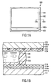
- Figs.1A and 1B show an exemplary structure of a conventional liquid crystal display device when both of the above-described frame-narrowing and reduction of the number of masks are realized.
- Fig.1A is a plan view of the device and
- Fig.1B is a cross sectional view of the device taken along a line IIIB-IIIB of Fig. 1A .
- this liquid crystal display device 100 is constructed of a display section 101 and a peripheral portion 102 around the display section 101.
- a circuit 103 provided with a display section driving circuit electrically connected to the display section 101 and a controller for controlling the driving circuit and the remaining three sides remain free, intended to enhance the effect of frame-narrowing.
- this liquid crystal display device 100 has a configuration that a liquid crystal material 141 is disposed between a driving substrate 111 and an opposite substrate 121 and the liquid crystal material 141 is sealed by a sealing member 131 provided in a boundary area between the display section 101 and the peripheral portion 102.
- a wiring layer 118a of indium tin oxide (ITO) and a wiring layer 118b of an alloy of molybdenum (Mo) and chromium (Cr) are formed and these layers extend to an edge of the driving substrate 111.
- An insulating layer 119 is formed on the wiring layer 118b and a flattening film 116 is formed inside the sealing member 131 on the insulating layer.
- the wiring layers 118a and 118b are created through patterning by means of a single mask.
- the material of the insulating layer 119 for example, silicon nitride (SiNx) is used considering adhesion to the material of the sealing member 131.
- the opposite substrate 121 is provided with an opposite electrode 124 that extends to or near to an edge of the opposite substrate 121 together with a light shielding film (black matrix) 122 and a color filter 123.
- the end (parting plane) 111a of the driving substrate 111 and the end 121a of the opposite substrate 121 form a so-called flush-structure.
- the driving substrate 111 is larger than the opposite substrate 121 so that the wiring layers 118a and 118b on the driving substrate side do not face the opposite electrode 124 on the opposite substrate side.
- the wiring layers 118a and 118b are disposed opposite to the opposite electrode 124 even at the edge of the substrate.
- US 6,323,924 B1 discloses the liquid crystal display device 200, which includes the liquid crystal layer 13 between the first an d second transparent insulating substrates 11 and 12, on which the aluminum ally film 14 is formed and the sealing material 19 is provided.
- the surface of the first substrate 11 is exposed by the slits 14a cut in the aluminum alloy film 14 to prevent peeling off of the planarizing insulation film 15 (referring to col. 3 1. 65 to col. 41. 23 and Fig. 5 of US 6,323,924 ).
- EP 1008896 A1 discloses the display panel PNL, which includes the upper and lower glass substrates SUB1, SUB2 and the liquid crystal layer LC therebetween.
- the organic layer PSV2 is formed on the lower glass substrates SUB 1 to enhance the flatness (referring to paragraphs [0044], [0071] and Fig. 6 of EP 1008896 A1 )
- EP 1111436 A2 discloses the reflective liquid crystal display element, which includes the lower substrate 101, the undulated layer 102, the reflective layer 103, the flattened layer 106, the transparent electrode 107, the sealant 108, the liquid crystal layer 109, the upper transparent substrate 110, the external circuit board 114 and the anisotropic conductive layer adhesive 115, in which the undulated layer 102 is not formed at the connection terminal between the lower substrate 101 side of the liquid crystal cell 111 and the external circuit board 114.
- the reliability of electric connection and physical connection of the terminal and transparent electrode 107 can be enhanced (referring to paragraphs [0017], [0032] and Fig. 1A of EP 1111436 A2 ).
- US 5,847,785 A discloses the liquid crystal display device, which includes the small substrates 50, 51 and the counter substrate 53 so as to seal therein the liquid crystal layer 54, the first seal material 520 1 made of a photo-setting resin formed along connecting sides between the liquid crystal panels, and the second seal material made of a thermosetting resin formed along other sides than the connecting sides.
- a hardening inferior of the seal material as well as a display inferior of the liquid crystal panel can be prevented (referring to col. 10 lines 55-67 and Fig. 7 of US 5,847,785 A ).
- the present invention has been implemented in view of the above-described problems and it is an object of the present invention to provide a liquid crystal display device capable of realizing miniaturization and cost reduction as well as providing high reliability, and more specifically, to provide a high reliability liquid crystal display device with corrosion of wiring layers in the peripheral portion suppressed.
- the liquid crystal display device comprises a first substrate having a first conductive member, a second substrate disposed opposite to the first substrate with a given space therebetween and having a second conductive member on its surface opposite to the first conductive member of the first substrate, a sealing member disposed between the first substrate and the second substrate and a liquid crystal layer formed by a liquid crystal material sealed by the sealing member in the space between the first substrate and the second substrate, characterized in that a side face of the first substrate and a side face of the second substrate corresponding to the side face of the first substrate are present substantially in the same plane, that the first conductive member extends to an edge of the side face of the first substrate, an end of the first conductive member on a side of the side face of the first substrate having a possibility to contact with the atmosphere, the second conductive member extending to or near to an edge of the side face of the second substrate, and that a dielectric member having a relative dielectric constant equal to or less than 5 is disposed between the first conductive member and the second conductive member at
- the liquid crystal display device is provided with a dielectric member having a relative dielectric constant equal to or less than 5 between the first conductive member and the second conductive member on the side of the sealing member remote from the liquid crystal layer, a potential difference between the first conductive member and second conductive member becomes relatively smaller during driving and the electric field produced therebetween is reduced. For this reason, corrosion of the part of the end of the first conductive member that has contact with the atmosphere is suppresses and the device has high reliability.
- the dielectric member extends to the edge of the side face of the first substrate. This suppresses corrosion of the first conductive member more effectively, and can thereby further improve the reliability of the device.
- the first substrate is further provided with depressions or projections which are spaced apart from each other on the same side as that on which the first conductive member is provided, and a reflecting film which is rendered uneven under the influence of the depressions or projections and has a function of reflecting a light and that the dielectric member is provided so as to extend from the side of the sealing member remote from the liquid crystal layer to the side of the liquid crystal layer as an integral member, the dielectric member being disposed between the depressions or projections and the reflecting film on the liquid crystal layer's side of the sealing member.
- the dielectric member from the side of the sealing member remote from the liquid crystal layer to the side of the liquid crystal layer as an integral member allows a single layer to have each functions of the sealing member on the liquid crystal layer's side and the remote side of the sealing member. This simplifies the configuration of the device.
- the dielectric member is in contact with the sealing member and that the dielectric member is made of a resin and the sealing member is made of a thermosetting resin because this will enhance adhesion therebetween.
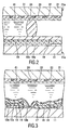
- Figs.2 and 3 show the liquid crystal display device according to this embodiment.
- the liquid crystal display device according to this embodiment is constructed of a display section and a peripheral portion peripheral to the display section as in the case of above-described Fig.1A and is provided with a circuit on one side of the peripheral portion.
- Fig.2 is a cross sectional view of the area of the peripheral portion where no circuit exists and its periphery
- Fig.3 is a cross sectional view of the display section.
- This liquid crystal display device is provided with a driving substrate 11 as a first substrate and an opposite substrate 21 as a second substrate disposed opposite to the driving substrate 11 with a given space therebetween and a sealing member 31 is disposed between the driving substrate 11 and the opposite substrate 21.
- a liquid crystal layer 41 is formed by a liquid crystal material sealed by the sealing member 31 in the space between the driving substrate 11 and the opposite substrate 21.
- the driving substrate 11 and the opposite substrate 21 form a so-called "flush-structure" in the area of the peripheral portion without any circuit ( Fig.2 ) in which their respective side faces 11a and 21a are present substantially in the same plane.
- the driving substrate 11 is provided, on its surface facing the opposite substrate, with source electrodes 12a electrically connected to respective data lines and drain electrodes 12b, with a space being disposed therebetween, and a semiconductor layer 12c is formed adjacent to the source electrodes 12a and the drain electrodes 12b.
- Gate electrodes 14 electrically connected to respective scanning lines are formed on the side of the semiconductor layer 12c remote from the driving substrate 11, with a gate insulating film 13 having an opening being formed between the semiconductor layer 12c and the gate electrodes 14.
- TFTs are provided on the side of the driving substrate 11 facing the opposite substrate 21.
- the TFTs are placed in a form of, for example, a matrix in a one-to-one correspondence with pixel electrodes, which will be described later.
- a pattern of depressions or projections 15 provided with a space therebetween is formed on the gate insulating film 13 and the gate electrode 14 and a flattening film 16 is provided, as a dielectric material, on the pattern of depressions or projections 15 with an opening.
- a reflecting film (reflecting electrode) 17 also functioning as a pixel electrode is formed on the flattening film 16.
- the reflecting film 17 is electrically connected, for example, with the drain electrodes 12b through the openings provided in the flattening film 16 and the gate insulating film 13 and voltages are applied thereto using the above-described TFTs.
- the driving substrate 11 is further provided with an orientation film (not shown), and so on.
- the wiring layers 18a and 18b are formed as the first conductive members on the side of the driving substrate 11 opposite to the opposite substrate 21 as shown in Fig.2 . These wiring layers 18a and 18b extend to an edge constituting the side face 11 a of the driving substrate 11, which has a possibility to contact with the atmosphere.
- the wiring layer 18a is made, for example, of ITO and used as a terminal of the display section.
- the wiring layer 18b is made, for example, of an alloy of molybdenum and chromium, forming a data line.
- the flattening film 16 extends, for example, to the edge constituting the side face 11 a of the driving substrate 11, with the insulating film 19 being formed between the wiring layer 18b and the flattening film 16.
- the above-described components on the driving substrate 11 are created in such a way that, for example, the source electrodes 12a, the drain electrodes 12b and the wiring layers 18a and 18b are patterned, the semiconductor layer 12c is patterned, the gate insulating film 13 is patterned, and then the gate electrodes 14, depressions or projections 15, the flattening film 16 and the reflecting electrode 17 are patterned one by one.
- a light shielding film 22, a color filter 23, the opposite electrode 24 as the second conductive member and an orientation film (not shown), etc., are formed on the surface of the opposite substrate 21 facing the driving substrate side.
- the opposite electrode 24 extends to or near to the edge of the side face 21a of the opposite substrate 21 (near the edge in Fig.2 ).
- a polarizing plate, etc. is formed on the side of the opposite substrate 21 remote from the driving substrate 11.
- the flattening film 16 which constitutes a characteristic portion of the liquid crystal display device according to this embodiment, will be explained in more detail below.
- the flattening film 16 is made of a dielectric member having a relative dielectric constant equal to or less than 5, or more preferably equal to or less than 3.5, for example, 2 to 3.5, and more specifically made of, for example, a resin. This flattening film 16 is intended to adjust unevenness of the reflecting film 17 rendered uneven by the patterned depressions or projections 15 (refer to Japanese Patent Application No. 2001-308737 ).
- the flattening film 16 made of the above-described dielectric member is disposed up to an edge of the driving substrate 11 and inserted between the wiring layers 18a and 18b and the opposite electrode 24, each extending to the edge of the substrate, and therefore a potential difference between the wiring layers 18a and 18b and opposite electrode 24 during driving is relatively small and the intensity of the electric field therebetween is also small.
- the relative dielectric constant of the dielectric member constituting the flattening film 16 the more preferable.
- the reason that the relative dielectric constant is set to be equal to or less than 5 is that with a relative dielectric constant exceeding 5, it would be impossible to obtain a sufficient effect unless the film thickness is increased considerably.
- the thickness of the flattening film 16 is, for example, 1 ⁇ m to 5 ⁇ m.
- the sealing member is provided on and in contact with the flattening film 16 and the level of adhesion between the flattening film 16 and the sealing member 31 is required to be high. For this reason, when the resin is used as the material of the flattening film 16, it is preferable to use a thermosetting resin for the sealing member 31.
- the liquid crystal display device with the above-described configuration will operate as follows.
- a scanning voltage is sequentially supplied from the circuit to the gate lines through the wiring layer 18a cyclically and signal voltages are selectively supplied to the respective wiring layers 18b (data lines) in accordance with image signals.
- a given voltage is constantly supplied to the opposite electrode 24.
- the signal voltages are supplied to the reflecting electrodes (pixel electrodes) 17 through TFTs which have turned on with a scanning voltage supplied sequentially, which provides a voltage to the liquid crystal layer 41 between the opposite electrode 24 and the reflecting electrode 17 and allows a desired image display to be performed.
- the flattening film 16 made of a dielectric member having a relative dielectric constant equal to or less than 5 is formed between the wiring layers 18a and 18b and the opposite electrode 24 in the area of the peripheral portion where no circuit exists, the potential difference between the wiring layers 18a and 18b and the opposite electrode 24 becomes relatively smaller and the electric field produced therebetween is reduced. This suppresses corrosion of the areas of the wiring layers 18a and 18b in contact with the atmosphere.
- the liquid crystal display device is provided with the flattening film 16 made of a dielectric member having a relative dielectric constant equal to or less than 5 between the wiring layers 18a and 18b and the opposite electrode 24, and can thereby reduce the potential difference between the mutually facing wiring layers 18a and 18b and opposite electrode 24 in the area of the peripheral portion where no circuit exists when a voltage is applied to the wiring layers 18a and 18b and the opposite electrode 24 and reduce the electric field produced therebetween due to this potential difference. Therefore, even when the ends of the wiring layers 18a and 18b contact with the atmosphere, a reaction between the wiring layers 18a and 18b and water, etc., in the atmosphere is suppressed so that the corrosion rate of the wiring layers 18a and 18b can be reduced considerably.
- this embodiment can implement a small, highly reliable liquid crystal display device in fewer patterning steps and make the device highly reliable even in a high temperature, high humidity operating environment in particular.
- the flattening film for adjusting unevenness on the surface of the reflecting film 17 is further extended to insert the dielectric member between the wiring layers 18a and 18b and the opposite electrode 24, it is possible to suppress corrosion of the wiring layers 18a and 18b with a simple structure without providing any additional film, realizing cost reduction in this respect, too.
- composing the flattening film 16 of a resin and composing the sealing member 17 of a thermosetting resin can enhance adhesion between the flattening film 16 and the sealing member 17 and thereby implement a high reliability liquid crystal display device.
- the present invention has been explained with reference to the embodiment, but the present invention is not limited to the above-described embodiment and can be modified in various ways.
- the above-described embodiment has described the case where the flattening film necessary inside the display section is extended to an edge of the driving substrate, but it is also possible to insert a dielectric member, in the peripheral portion, between the wiring layers 18a and 18b and the opposite electrode 24 aside from the flattening film 16.
- the above-described dielectric member need not necessarily be extended to an edge of the substrate, but the effect of the present invention can be obtained when the dielectric member is provided into, in the peripheral portion, at least a part between the wiring layers 18a and 18b and the opposite electrode 24.
- the above-described embodiment has described an example of the first conductive member having a multilayer structure consisting of the wiring layers 18a and 18b, but the first conductive member can also have a single-layer structure.
- the second conductive member may have a multilayer structure.
- the above-described embodiment has described an example of a patterning method on the driving substrate, but the present invention is also effective for a device manufactured using any method other the above-described patterning method if the device has a structure that the end faces of the wiring layers 18a and 18b contact with the atmosphere.
- the above-described embodiment has described the liquid crystal display device provided with so-called top gate type TFTs, but the device can also be adapted so as to have so-called bottom gate type TFTs. Furthermore, the above-described embodiment has described the liquid crystal display device with an active matrix display using TFTs as switching elements, but the device can also be adapted so as to have other switching elements such as MOSFET (metal oxide semiconductor field effect transistor). Moreover, the present invention is also applicable to a passive matrix display device without using any switching element.
- MOSFET metal oxide semiconductor field effect transistor
- the present invention is also applicable to a liquid crystal display device having a combined structure of a reflective type and transmission type or a liquid crystal display device with the reflecting film 17 whose thickness is reduced so as to reflect part of light and allow part of light to penetrate.
- the present invention is also applicable to a transmission type liquid crystal display device, in which case a flattening film provided on the driving substrate to increase an open area ratio can also be used in the same way as the above-described flattening film 16.
Abstract
Description
- The present invention relates to a liquid crystal display device in which a liquid crystal material is sealed by a sealing member between a first substrate having a first conductive member and a second substrate having a second conductive member, and more particularly, to a narrow-framed liquid crystal display device whose area other than the display area is reduced.
- With electronic devices provided with a liquid crystal display device represented by a cellular phone and personal computer getting rapidly widespread in recent years, there is a strong demand for a liquid crystal display device realizing miniaturization and cost reduction. While there is such a strong demand for miniaturization of the entire device, there is another demand that the area of the display section should be expanded. For this purpose, a process of narrowing the width of the portion peripheral to the display section (frame section), or so-called "frame-narrowing" is underway. The peripheral portion is a space disposed with wiring for supplying power to TFTs (thin film transistors) used for switching of a liquid crystal material and terminals for bonding IC chips making up a driving circuit and this space is conventionally disposed with circuits on all the peripheral portions at the upper edge, lower edge, right edge and left edge. However, with the progress of frame-narrowing, the circuits are recently provided only on the lower peripheral portion. On the other hand, with respect to the demand for cost reduction, there is a demand for a reduction of the number of masks at the manufacturing stage. In response to this demand, patterning of layers made of different materials is realized with a single mask.
-
Figs.1A and 1B show an exemplary structure of a conventional liquid crystal display device when both of the above-described frame-narrowing and reduction of the number of masks are realized.Fig.1A is a plan view of the device andFig.1B is a cross sectional view of the device taken along a line IIIB-IIIB ofFig. 1A . When viewed from the top, this liquidcrystal display device 100 is constructed of adisplay section 101 and aperipheral portion 102 around thedisplay section 101. On the lowerperipheral portion 102a of theperipheral portion 102, there is acircuit 103 provided with a display section driving circuit electrically connected to thedisplay section 101 and a controller for controlling the driving circuit and the remaining three sides remain free, intended to enhance the effect of frame-narrowing. - As shown in
Fig.1B , this liquidcrystal display device 100 has a configuration that aliquid crystal material 141 is disposed between adriving substrate 111 and anopposite substrate 121 and theliquid crystal material 141 is sealed by asealing member 131 provided in a boundary area between thedisplay section 101 and theperipheral portion 102. On thedriving substrate 111, awiring layer 118a of indium tin oxide (ITO) and awiring layer 118b of an alloy of molybdenum (Mo) and chromium (Cr) are formed and these layers extend to an edge of thedriving substrate 111. Aninsulating layer 119 is formed on thewiring layer 118b and aflattening film 116 is formed inside the sealingmember 131 on the insulating layer. Thewiring layers insulating layer 119, for example, silicon nitride (SiNx) is used considering adhesion to the material of the sealingmember 131. On the other hand, theopposite substrate 121 is provided with anopposite electrode 124 that extends to or near to an edge of theopposite substrate 121 together with a light shielding film (black matrix) 122 and acolor filter 123. - In the liquid
crystal display device 100, at the peripheral portion in the above-described free state, that is, the area where no circuit exists, the end (parting plane) 111a of thedriving substrate 111 and theend 121a of theopposite substrate 121 form a so-called flush-structure. At the lowerperipheral portion 102a provided with thecircuit 103 of theperipheral portion 102, thedriving substrate 111 is larger than theopposite substrate 121 so that thewiring layers opposite electrode 124 on the opposite substrate side. However, in the area where no circuit exists, thewiring layers opposite electrode 124 even at the edge of the substrate. In this area, the ends of thewiring layers wiring layers wiring layers opposite electrode 124 facing mutually due to a potential difference therebetween, and the portions of thewiring layers wiring layers -
US 6,323,924 B1 discloses the liquid crystal display device 200, which includes theliquid crystal layer 13 between the first an d secondtransparent insulating substrates 11 and 12, on which thealuminum ally film 14 is formed and thesealing material 19 is provided. The surface of thefirst substrate 11 is exposed by the slits 14a cut in thealuminum alloy film 14 to prevent peeling off of the planarizing insulation film 15 (referring to col. 3 1. 65 to col. 41. 23 and Fig. 5 ofUS 6,323,924 ). -
EP 1008896 A1 discloses the display panel PNL, which includes the upper and lower glass substrates SUB1, SUB2 and the liquid crystal layer LC therebetween. The organic layer PSV2 is formed on the lower glass substrates SUB 1 to enhance the flatness (referring to paragraphs [0044], [0071] and Fig. 6 ofEP 1008896 A1 ) -
EP 1111436 A2 discloses the reflective liquid crystal display element, which includes thelower substrate 101, the undulatedlayer 102, thereflective layer 103, the flattened layer 106, the transparent electrode 107, the sealant 108, the liquid crystal layer 109, the upper transparent substrate 110, the external circuit board 114 and the anisotropic conductive layer adhesive 115, in which the undulatedlayer 102 is not formed at the connection terminal between thelower substrate 101 side of theliquid crystal cell 111 and the external circuit board 114. Hence, the reliability of electric connection and physical connection of the terminal and transparent electrode 107 can be enhanced (referring to paragraphs [0017], [0032] andFig. 1A ofEP 1111436 A2 ). -
US 5,847,785 A discloses the liquid crystal display device, which includes the small substrates 50, 51 and the counter substrate 53 so as to seal therein the liquid crystal layer 54, the first seal material 520 1 made of a photo-setting resin formed along connecting sides between the liquid crystal panels, and the second seal material made of a thermosetting resin formed along other sides than the connecting sides. As a result, a hardening inferior of the seal material as well as a display inferior of the liquid crystal panel can be prevented (referring to col. 10 lines 55-67 and Fig. 7 ofUS 5,847,785 A ). - The present invention has been implemented in view of the above-described problems and it is an object of the present invention to provide a liquid crystal display device capable of realizing miniaturization and cost reduction as well as providing high reliability, and more specifically, to provide a high reliability liquid crystal display device with corrosion of wiring layers in the peripheral portion suppressed.
- The liquid crystal display device according to the present invention comprises a first substrate having a first conductive member, a second substrate disposed opposite to the first substrate with a given space therebetween and having a second conductive member on its surface opposite to the first conductive member of the first substrate, a sealing member disposed between the first substrate and the second substrate and a liquid crystal layer formed by a liquid crystal material sealed by the sealing member in the space between the first substrate and the second substrate, characterized in that a side face of the first substrate and a side face of the second substrate corresponding to the side face of the first substrate are present substantially in the same plane, that the first conductive member extends to an edge of the side face of the first substrate, an end of the first conductive member on a side of the side face of the first substrate having a possibility to contact with the atmosphere, the second conductive member extending to or near to an edge of the side face of the second substrate, and that a dielectric member having a relative dielectric constant equal to or less than 5 is disposed between the first conductive member and the second conductive member at least on the side of the sealing member remote from the liquid crystal layer.
- Since the liquid crystal display device according to the present invention is provided with a dielectric member having a relative dielectric constant equal to or less than 5 between the first conductive member and the second conductive member on the side of the sealing member remote from the liquid crystal layer, a potential difference between the first conductive member and second conductive member becomes relatively smaller during driving and the electric field produced therebetween is reduced. For this reason, corrosion of the part of the end of the first conductive member that has contact with the atmosphere is suppresses and the device has high reliability.
- Furthermore, for the liquid crystal display device according to the present invention, it is preferable that the dielectric member extends to the edge of the side face of the first substrate. This suppresses corrosion of the first conductive member more effectively, and can thereby further improve the reliability of the device.
- Furthermore, for the liquid crystal display device according to the present invention, it is preferable that the first substrate is further provided with depressions or projections which are spaced apart from each other on the same side as that on which the first conductive member is provided, and a reflecting film which is rendered uneven under the influence of the depressions or projections and has a function of reflecting a light and that the dielectric member is provided so as to extend from the side of the sealing member remote from the liquid crystal layer to the side of the liquid crystal layer as an integral member, the dielectric member being disposed between the depressions or projections and the reflecting film on the liquid crystal layer's side of the sealing member. In the case of such a reflective type liquid crystal display device, providing the dielectric member from the side of the sealing member remote from the liquid crystal layer to the side of the liquid crystal layer as an integral member allows a single layer to have each functions of the sealing member on the liquid crystal layer's side and the remote side of the sealing member. This simplifies the configuration of the device. In this case, it is preferable that the dielectric member is in contact with the sealing member and that the dielectric member is made of a resin and the sealing member is made of a thermosetting resin because this will enhance adhesion therebetween.
-
-
Fig. 1A is a plan view of a conventional exemplary liquid crystal display device, andFig. 1B is a cross sectional view of the device taken along a line IIIB-IIIB ofFig. 1A . -
Fig. 2 is a cross sectional view of a liquid crystal display device according to an embodiment of the invention; -
Fig. 3 is another cross sectional view of the liquid crystal display device according to the embodiment of the invention; - With reference now to the accompanying drawings, an embodiment of the present invention will be described in detail below.
- First, a configuration of a liquid crystal display device according to an embodiment of the present invention will be explained.
Figs.2 and 3 show the liquid crystal display device according to this embodiment. When viewed from the top, the liquid crystal display device according to this embodiment is constructed of a display section and a peripheral portion peripheral to the display section as in the case of above-describedFig.1A and is provided with a circuit on one side of the peripheral portion.Fig.2 is a cross sectional view of the area of the peripheral portion where no circuit exists and its periphery, andFig.3 is a cross sectional view of the display section. - This liquid crystal display device is provided with a
driving substrate 11 as a first substrate and anopposite substrate 21 as a second substrate disposed opposite to thedriving substrate 11 with a given space therebetween and asealing member 31 is disposed between thedriving substrate 11 and theopposite substrate 21. Aliquid crystal layer 41 is formed by a liquid crystal material sealed by the sealingmember 31 in the space between the drivingsubstrate 11 and theopposite substrate 21. The drivingsubstrate 11 and theopposite substrate 21 form a so-called "flush-structure" in the area of the peripheral portion without any circuit (Fig.2 ) in which their respective side faces 11a and 21a are present substantially in the same plane. - In the display section, as shown in
Fig.3 , the drivingsubstrate 11 is provided, on its surface facing the opposite substrate, withsource electrodes 12a electrically connected to respective data lines anddrain electrodes 12b, with a space being disposed therebetween, and asemiconductor layer 12c is formed adjacent to thesource electrodes 12a and thedrain electrodes 12b.Gate electrodes 14 electrically connected to respective scanning lines (not shown) are formed on the side of thesemiconductor layer 12c remote from the drivingsubstrate 11, with agate insulating film 13 having an opening being formed between thesemiconductor layer 12c and thegate electrodes 14. Thus, TFTs are provided on the side of the drivingsubstrate 11 facing theopposite substrate 21. The TFTs are placed in a form of, for example, a matrix in a one-to-one correspondence with pixel electrodes, which will be described later. A pattern of depressions orprojections 15 provided with a space therebetween is formed on thegate insulating film 13 and thegate electrode 14 and a flatteningfilm 16 is provided, as a dielectric material, on the pattern of depressions orprojections 15 with an opening. A reflecting film (reflecting electrode) 17 also functioning as a pixel electrode is formed on the flatteningfilm 16. The reflectingfilm 17 is electrically connected, for example, with thedrain electrodes 12b through the openings provided in the flatteningfilm 16 and thegate insulating film 13 and voltages are applied thereto using the above-described TFTs. The drivingsubstrate 11 is further provided with an orientation film (not shown), and so on. - Furthermore, in the area or in the vicinity of the peripheral portion of this liquid crystal display device where no circuit exists, the wiring layers 18a and 18b are formed as the first conductive members on the side of the driving
substrate 11 opposite to theopposite substrate 21 as shown inFig.2 . These wiring layers 18a and 18b extend to an edge constituting the side face 11 a of the drivingsubstrate 11, which has a possibility to contact with the atmosphere. Thewiring layer 18a is made, for example, of ITO and used as a terminal of the display section. Thewiring layer 18b is made, for example, of an alloy of molybdenum and chromium, forming a data line. On the wiring layers 18a and 18b, the flatteningfilm 16 extends, for example, to the edge constituting the side face 11 a of the drivingsubstrate 11, with the insulatingfilm 19 being formed between thewiring layer 18b and the flatteningfilm 16. - The above-described components on the driving
substrate 11 are created in such a way that, for example, thesource electrodes 12a, thedrain electrodes 12b and the wiring layers 18a and 18b are patterned, thesemiconductor layer 12c is patterned, thegate insulating film 13 is patterned, and then thegate electrodes 14, depressions orprojections 15, the flatteningfilm 16 and the reflectingelectrode 17 are patterned one by one. - On the other hand, a
light shielding film 22, acolor filter 23, theopposite electrode 24 as the second conductive member and an orientation film (not shown), etc., are formed on the surface of theopposite substrate 21 facing the driving substrate side. Theopposite electrode 24 extends to or near to the edge of theside face 21a of the opposite substrate 21 (near the edge inFig.2 ). Though not shown here, a polarizing plate, etc., is formed on the side of theopposite substrate 21 remote from the drivingsubstrate 11. - Secondly, the flattening
film 16, which constitutes a characteristic portion of the liquid crystal display device according to this embodiment, will be explained in more detail below. - The flattening
film 16 is made of a dielectric member having a relative dielectric constant equal to or less than 5, or more preferably equal to or less than 3.5, for example, 2 to 3.5, and more specifically made of, for example, a resin. This flatteningfilm 16 is intended to adjust unevenness of the reflectingfilm 17 rendered uneven by the patterned depressions or projections 15 (refer to Japanese Patent Application No.2001-308737 film 16 made of the above-described dielectric member is disposed up to an edge of the drivingsubstrate 11 and inserted between the wiring layers 18a and 18b and theopposite electrode 24, each extending to the edge of the substrate, and therefore a potential difference between the wiring layers 18a and 18b andopposite electrode 24 during driving is relatively small and the intensity of the electric field therebetween is also small. Considering the function as the dielectric in such a peripheral portion of the apparatus, the smaller the relative dielectric constant of the dielectric member constituting the flatteningfilm 16, the more preferable. The reason that the relative dielectric constant is set to be equal to or less than 5 is that with a relative dielectric constant exceeding 5, it would be impossible to obtain a sufficient effect unless the film thickness is increased considerably. The thickness of the flatteningfilm 16 is, for example, 1 µm to 5 µm. - In this embodiment, the sealing member is provided on and in contact with the flattening
film 16 and the level of adhesion between the flatteningfilm 16 and the sealingmember 31 is required to be high. For this reason, when the resin is used as the material of the flatteningfilm 16, it is preferable to use a thermosetting resin for the sealingmember 31. - The liquid crystal display device with the above-described configuration will operate as follows.
- In this liquid crystal display device, a scanning voltage is sequentially supplied from the circuit to the gate lines through the
wiring layer 18a cyclically and signal voltages are selectively supplied to therespective wiring layers 18b (data lines) in accordance with image signals. A given voltage is constantly supplied to theopposite electrode 24. The signal voltages are supplied to the reflecting electrodes (pixel electrodes) 17 through TFTs which have turned on with a scanning voltage supplied sequentially, which provides a voltage to theliquid crystal layer 41 between theopposite electrode 24 and the reflectingelectrode 17 and allows a desired image display to be performed. - In this case, since the flattening
film 16 made of a dielectric member having a relative dielectric constant equal to or less than 5 is formed between the wiring layers 18a and 18b and theopposite electrode 24 in the area of the peripheral portion where no circuit exists, the potential difference between the wiring layers 18a and 18b and theopposite electrode 24 becomes relatively smaller and the electric field produced therebetween is reduced. This suppresses corrosion of the areas of the wiring layers 18a and 18b in contact with the atmosphere. - As described above, the liquid crystal display device according to this embodiment is provided with the flattening
film 16 made of a dielectric member having a relative dielectric constant equal to or less than 5 between the wiring layers 18a and 18b and theopposite electrode 24, and can thereby reduce the potential difference between the mutually facingwiring layers opposite electrode 24 in the area of the peripheral portion where no circuit exists when a voltage is applied to the wiring layers 18a and 18b and theopposite electrode 24 and reduce the electric field produced therebetween due to this potential difference. Therefore, even when the ends of the wiring layers 18a and 18b contact with the atmosphere, a reaction between the wiring layers 18a and 18b and water, etc., in the atmosphere is suppressed so that the corrosion rate of the wiring layers 18a and 18b can be reduced considerably. Thus, this embodiment can implement a small, highly reliable liquid crystal display device in fewer patterning steps and make the device highly reliable even in a high temperature, high humidity operating environment in particular. - Furthermore, with the above-mentioned liquid crystal display device, since the flattening film for adjusting unevenness on the surface of the reflecting
film 17 is further extended to insert the dielectric member between the wiring layers 18a and 18b and theopposite electrode 24, it is possible to suppress corrosion of the wiring layers 18a and 18b with a simple structure without providing any additional film, realizing cost reduction in this respect, too. - Furthermore, composing the flattening
film 16 of a resin and composing the sealingmember 17 of a thermosetting resin can enhance adhesion between the flatteningfilm 16 and the sealingmember 17 and thereby implement a high reliability liquid crystal display device. - The present invention has been explained with reference to the embodiment, but the present invention is not limited to the above-described embodiment and can be modified in various ways. For example, the above-described embodiment has described the case where the flattening film necessary inside the display section is extended to an edge of the driving substrate, but it is also possible to insert a dielectric member, in the peripheral portion, between the wiring layers 18a and 18b and the
opposite electrode 24 aside from the flatteningfilm 16. Moreover, the above-described dielectric member need not necessarily be extended to an edge of the substrate, but the effect of the present invention can be obtained when the dielectric member is provided into, in the peripheral portion, at least a part between the wiring layers 18a and 18b and theopposite electrode 24. - Furthermore, the above-described embodiment has described an example of the first conductive member having a multilayer structure consisting of the wiring layers 18a and 18b, but the first conductive member can also have a single-layer structure. The second conductive member may have a multilayer structure.
- Furthermore, the above-described embodiment has described an example of a patterning method on the driving substrate, but the present invention is also effective for a device manufactured using any method other the above-described patterning method if the device has a structure that the end faces of the wiring layers 18a and 18b contact with the atmosphere.
- Furthermore, the above-described embodiment has described the liquid crystal display device provided with so-called top gate type TFTs, but the device can also be adapted so as to have so-called bottom gate type TFTs. Furthermore, the above-described embodiment has described the liquid crystal display device with an active matrix display using TFTs as switching elements, but the device can also be adapted so as to have other switching elements such as MOSFET (metal oxide semiconductor field effect transistor). Moreover, the present invention is also applicable to a passive matrix display device without using any switching element.
- Furthermore, the above-described embodiment has described the reflective type liquid crystal display device, but the present invention is also applicable to a liquid crystal display device having a combined structure of a reflective type and transmission type or a liquid crystal display device with the reflecting
film 17 whose thickness is reduced so as to reflect part of light and allow part of light to penetrate. In addition, the present invention is also applicable to a transmission type liquid crystal display device, in which case a flattening film provided on the driving substrate to increase an open area ratio can also be used in the same way as the above-describedflattening film 16.
Claims (5)
- A liquid crystal display device comprising:a first substrate (11) having a first conductive wiring member (18a, 18b);a second substrate (21) disposed opposite to the first substrate (11) with a given space therebetween and having a second conductive member (24) on its surface opposite to the first conductive member (18a, 18b) of the first substrate (11); a sealing member (31) disposed between the first substrate (11) and the second substrate (21); anda liquid crystal layer (41) formed by a liquid crystal material sealed by the sealing member (31) in the space between the first substrate (11) and the second substrate (21),a side face (11a) of the first substrate (11) and a corresponding side face (21a) of the second substrate (21) corresponding to said side face (11a) of the first substrate (11) which are present substantially in the same plane;wherein the first conductive member (18a, 18b) extends to an edge of said side face (11a) of the first substrate (11), the end face of the first conductive member (18a, 18b) on a side of said side face (11a) of the first substrate (11) being in contact with the atmosphere, the second conductive member (24) extending to or near said side face (21 a) of the second substrate (21); and characterized in thatthe first substrate (11) is further provided with depressions or projections (15) which are spaced apart from each other and arranged on the same side of the first substrate as that on which the first conductive member (18a, 18b) is provided, and a reflective film (17) which is rendered uneven under the influence of the depressions or projections (15) and has a function of reflecting a light;and in that a dielectric member (16) having a relative dielectric constant equal to or less than 5 is disposed between the first conductive member (18a, 18b) and the second conductive member (24) at least on the side of the sealing member (31) remote from the liquid crystal layer (41), and the dielectric member (16) is disposed between the depressions or projections (15) and the reflective film (17) on the liquid crystal layer's (41) side of the sealing member(31).
- A liquid crystal display device as Claimed in claim 1, characterized in that the dielectric member (16) extends to the edge of the side face (11a) of the first substrate (11).
- A liquid crystal display device as claimed in claim 1 or 2, characterized:in that the dielectric member (16) is provided so as to extend from the side of the sealing member (31) remote from the liquid crystal layer (41) to the side of the liquid crystal layer (41) as an integral member.
- A liquid crystal display device as claimed in claim 3, characterized in that the dielectric member (16) is in contact with the sealing member (31).
- A liquid crystal display device as claimed in claim 4, characterized in that the dielectric member (16) is made of a resin and the sealing member (31) is made of a thermosetting resin.
Applications Claiming Priority (3)
| Application Number | Priority Date | Filing Date | Title |
|---|---|---|---|
| JP2002035946A JP2003241215A (en) | 2002-02-13 | 2002-02-13 | Liquid crystal display device |
| JP2002035946 | 2002-02-13 | ||
| PCT/IB2003/000569 WO2003069401A1 (en) | 2002-02-13 | 2003-02-12 | Liquid crystal display device |
Publications (2)
| Publication Number | Publication Date |
|---|---|
| EP1478971A1 EP1478971A1 (en) | 2004-11-24 |
| EP1478971B1 true EP1478971B1 (en) | 2008-12-31 |
Family
ID=27678070
Family Applications (1)
| Application Number | Title | Priority Date | Filing Date |
|---|---|---|---|
| EP03702881A Expired - Lifetime EP1478971B1 (en) | 2002-02-13 | 2003-02-12 | Liquid crystal display device |
Country Status (10)
| Country | Link |
|---|---|
| US (1) | US20050146666A1 (en) |
| EP (1) | EP1478971B1 (en) |
| JP (1) | JP2003241215A (en) |
| KR (1) | KR20040076291A (en) |
| CN (1) | CN100403149C (en) |
| AT (1) | ATE419556T1 (en) |
| AU (1) | AU2003205998A1 (en) |
| DE (1) | DE60325559D1 (en) |
| TW (1) | TW200304019A (en) |
| WO (1) | WO2003069401A1 (en) |
Families Citing this family (4)
| Publication number | Priority date | Publication date | Assignee | Title |
|---|---|---|---|---|
| WO2007032395A1 (en) * | 2005-09-15 | 2007-03-22 | Sharp Kabushiki Kaisha | Display panel |
| CN104460070B (en) * | 2014-12-31 | 2018-09-07 | 合肥鑫晟光电科技有限公司 | Display panel and preparation method thereof, display device |
| CN105068328A (en) * | 2015-09-22 | 2015-11-18 | 武汉华星光电技术有限公司 | Method for manufacturing liquid-crystal display screen and liquid-crystal display screen |
| CN105467661A (en) * | 2016-01-13 | 2016-04-06 | 京东方科技集团股份有限公司 | Color film substrate and making method thereof, liquid crystal display panel and display device |
Family Cites Families (7)
| Publication number | Priority date | Publication date | Assignee | Title |
|---|---|---|---|---|
| US6288764B1 (en) * | 1996-06-25 | 2001-09-11 | Semiconductor Energy Laboratory Co., Ltd. | Display device or electronic device having liquid crystal display panel |
| US5953094A (en) | 1997-04-04 | 1999-09-14 | Sanyo Electric Co., Ltd. | Liquid crystal display device |
| WO1998047044A1 (en) * | 1997-04-11 | 1998-10-22 | Hitachi, Ltd. | Liquid crystal display device |
| JP3483730B2 (en) * | 1997-05-21 | 2004-01-06 | シャープ株式会社 | Liquid crystal display |
| US6335779B1 (en) * | 1999-01-27 | 2002-01-01 | Mistubishi Denki Kaubshiki Kaisha | Liquid crystal display apparatus and method for producing TFT using therefor |
| KR100407413B1 (en) * | 1999-07-19 | 2003-11-28 | 마쯔시다덴기산교 가부시키가이샤 | Reflector, method of fabricating the same, reflective display device comprising reflector, and method of fabricating the same |
| TW526357B (en) * | 1999-12-22 | 2003-04-01 | Matsushita Electric Ind Co Ltd | Reflective liquid crystal display element and image display device using the same |
-
2002
- 2002-02-13 JP JP2002035946A patent/JP2003241215A/en active Pending
-
2003
- 2003-02-11 TW TW092102752A patent/TW200304019A/en unknown
- 2003-02-12 KR KR10-2004-7012446A patent/KR20040076291A/en not_active Application Discontinuation
- 2003-02-12 EP EP03702881A patent/EP1478971B1/en not_active Expired - Lifetime
- 2003-02-12 DE DE60325559T patent/DE60325559D1/en not_active Expired - Lifetime
- 2003-02-12 AT AT03702881T patent/ATE419556T1/en not_active IP Right Cessation
- 2003-02-12 US US10/504,336 patent/US20050146666A1/en not_active Abandoned
- 2003-02-12 WO PCT/IB2003/000569 patent/WO2003069401A1/en active Application Filing
- 2003-02-12 CN CNB038038005A patent/CN100403149C/en not_active Expired - Lifetime
- 2003-02-12 AU AU2003205998A patent/AU2003205998A1/en not_active Abandoned
Also Published As
| Publication number | Publication date |
|---|---|
| ATE419556T1 (en) | 2009-01-15 |
| AU2003205998A1 (en) | 2003-09-04 |
| TW200304019A (en) | 2003-09-16 |
| EP1478971A1 (en) | 2004-11-24 |
| CN100403149C (en) | 2008-07-16 |
| DE60325559D1 (en) | 2009-02-12 |
| WO2003069401A1 (en) | 2003-08-21 |
| US20050146666A1 (en) | 2005-07-07 |
| CN1633621A (en) | 2005-06-29 |
| JP2003241215A (en) | 2003-08-27 |
| KR20040076291A (en) | 2004-08-31 |
Similar Documents
| Publication | Publication Date | Title |
|---|---|---|
| KR100763408B1 (en) | liquid crystal display devices | |
| US10216053B2 (en) | Amorphous silicon thin film transistor-liquid crystal display device and method of manufacturing the same | |
| US6937314B2 (en) | Liquid crystal display having terminals arranged for securing connection to driving circuit | |
| US5798812A (en) | Active matrix substrate and display device using the same with extending protrusions between gate and source line terminals | |
| KR100302577B1 (en) | Semiconductor device and method for producing the same | |
| US6028652A (en) | Array substrate for display device and manufacturing method thereof | |
| US7855767B2 (en) | Transflective liquid crystal display | |
| US20090086148A1 (en) | Display Device | |
| KR100724831B1 (en) | Active matrix substrate and method of manufacturing the same | |
| US7521298B2 (en) | Thin film transistor array panel of active liquid crystal display and fabrication method thereof | |
| EP1478971B1 (en) | Liquid crystal display device | |
| US20040041152A1 (en) | Electro-optical device and semiconductor device | |
| US8773341B2 (en) | Liquid crystal display device | |
| US20220278138A1 (en) | Array substrate, display panel, and display device | |
| JP4253181B2 (en) | Image display panel, photomask, image display device, and method for manufacturing image display panel | |
| US20060046374A1 (en) | Conducting line terminal structure for display device | |
| KR100508025B1 (en) | Substrate for liquid crystal display device having color filter and manufacturing method thereof | |
| KR20040098869A (en) | Pad structure of liquid crystal display | |
| JPH10206868A (en) | Color liquid crystal display device |
Legal Events
| Date | Code | Title | Description |
|---|---|---|---|
| PUAI | Public reference made under article 153(3) epc to a published international application that has entered the european phase |
Free format text: ORIGINAL CODE: 0009012 |
|
| 17P | Request for examination filed |
Effective date: 20040913 |
|
| AK | Designated contracting states |
Kind code of ref document: A1 Designated state(s): AT BE BG CH CY CZ DE DK EE ES FI FR GB GR HU IE IT LI LU MC NL PT SE SI SK TR |
|
| AX | Request for extension of the european patent |
Extension state: AL LT LV MK RO |
|
| RAP1 | Party data changed (applicant data changed or rights of an application transferred) |
Owner name: TPO HONG KONG HOLDING LIMITED |
|
| 17Q | First examination report despatched |
Effective date: 20071220 |
|
| GRAP | Despatch of communication of intention to grant a patent |
Free format text: ORIGINAL CODE: EPIDOSNIGR1 |
|
| GRAS | Grant fee paid |
Free format text: ORIGINAL CODE: EPIDOSNIGR3 |
|
| GRAA | (expected) grant |
Free format text: ORIGINAL CODE: 0009210 |
|
| AK | Designated contracting states |
Kind code of ref document: B1 Designated state(s): AT BE BG CH CY CZ DE DK EE ES FI FR GB GR HU IE IT LI LU MC NL PT SE SI SK TR |
|
| REG | Reference to a national code |
Ref country code: CH Ref legal event code: EP Ref country code: GB Ref legal event code: FG4D |
|
| REF | Corresponds to: |
Ref document number: 60325559 Country of ref document: DE Date of ref document: 20090212 Kind code of ref document: P |
|
| REG | Reference to a national code |
Ref country code: IE Ref legal event code: FG4D |
|
| PG25 | Lapsed in a contracting state [announced via postgrant information from national office to epo] |
Ref country code: FI Free format text: LAPSE BECAUSE OF FAILURE TO SUBMIT A TRANSLATION OF THE DESCRIPTION OR TO PAY THE FEE WITHIN THE PRESCRIBED TIME-LIMIT Effective date: 20081231 Ref country code: SI Free format text: LAPSE BECAUSE OF FAILURE TO SUBMIT A TRANSLATION OF THE DESCRIPTION OR TO PAY THE FEE WITHIN THE PRESCRIBED TIME-LIMIT Effective date: 20081231 |
|
| PG25 | Lapsed in a contracting state [announced via postgrant information from national office to epo] |
Ref country code: ES Free format text: LAPSE BECAUSE OF FAILURE TO SUBMIT A TRANSLATION OF THE DESCRIPTION OR TO PAY THE FEE WITHIN THE PRESCRIBED TIME-LIMIT Effective date: 20090411 Ref country code: BE Free format text: LAPSE BECAUSE OF FAILURE TO SUBMIT A TRANSLATION OF THE DESCRIPTION OR TO PAY THE FEE WITHIN THE PRESCRIBED TIME-LIMIT Effective date: 20081231 Ref country code: EE Free format text: LAPSE BECAUSE OF FAILURE TO SUBMIT A TRANSLATION OF THE DESCRIPTION OR TO PAY THE FEE WITHIN THE PRESCRIBED TIME-LIMIT Effective date: 20081231 |
|
| PG25 | Lapsed in a contracting state [announced via postgrant information from national office to epo] |
Ref country code: CZ Free format text: LAPSE BECAUSE OF FAILURE TO SUBMIT A TRANSLATION OF THE DESCRIPTION OR TO PAY THE FEE WITHIN THE PRESCRIBED TIME-LIMIT Effective date: 20081231 Ref country code: SE Free format text: LAPSE BECAUSE OF FAILURE TO SUBMIT A TRANSLATION OF THE DESCRIPTION OR TO PAY THE FEE WITHIN THE PRESCRIBED TIME-LIMIT Effective date: 20090331 Ref country code: PT Free format text: LAPSE BECAUSE OF FAILURE TO SUBMIT A TRANSLATION OF THE DESCRIPTION OR TO PAY THE FEE WITHIN THE PRESCRIBED TIME-LIMIT Effective date: 20090601 Ref country code: AT Free format text: LAPSE BECAUSE OF FAILURE TO SUBMIT A TRANSLATION OF THE DESCRIPTION OR TO PAY THE FEE WITHIN THE PRESCRIBED TIME-LIMIT Effective date: 20081231 |
|
| PG25 | Lapsed in a contracting state [announced via postgrant information from national office to epo] |
Ref country code: MC Free format text: LAPSE BECAUSE OF NON-PAYMENT OF DUE FEES Effective date: 20090228 Ref country code: SK Free format text: LAPSE BECAUSE OF FAILURE TO SUBMIT A TRANSLATION OF THE DESCRIPTION OR TO PAY THE FEE WITHIN THE PRESCRIBED TIME-LIMIT Effective date: 20081231 |
|
| REG | Reference to a national code |
Ref country code: CH Ref legal event code: PL |
|
| PG25 | Lapsed in a contracting state [announced via postgrant information from national office to epo] |
Ref country code: DK Free format text: LAPSE BECAUSE OF FAILURE TO SUBMIT A TRANSLATION OF THE DESCRIPTION OR TO PAY THE FEE WITHIN THE PRESCRIBED TIME-LIMIT Effective date: 20081231 Ref country code: LI Free format text: LAPSE BECAUSE OF NON-PAYMENT OF DUE FEES Effective date: 20090228 Ref country code: CH Free format text: LAPSE BECAUSE OF NON-PAYMENT OF DUE FEES Effective date: 20090228 |
|
| PLBE | No opposition filed within time limit |
Free format text: ORIGINAL CODE: 0009261 |
|
| STAA | Information on the status of an ep patent application or granted ep patent |
Free format text: STATUS: NO OPPOSITION FILED WITHIN TIME LIMIT |
|
| REG | Reference to a national code |
Ref country code: IE Ref legal event code: MM4A |
|
| 26N | No opposition filed |
Effective date: 20091001 |
|
| PG25 | Lapsed in a contracting state [announced via postgrant information from national office to epo] |
Ref country code: IE Free format text: LAPSE BECAUSE OF NON-PAYMENT OF DUE FEES Effective date: 20090212 Ref country code: BG Free format text: LAPSE BECAUSE OF FAILURE TO SUBMIT A TRANSLATION OF THE DESCRIPTION OR TO PAY THE FEE WITHIN THE PRESCRIBED TIME-LIMIT Effective date: 20090331 |
|
| PG25 | Lapsed in a contracting state [announced via postgrant information from national office to epo] |
Ref country code: GR Free format text: LAPSE BECAUSE OF FAILURE TO SUBMIT A TRANSLATION OF THE DESCRIPTION OR TO PAY THE FEE WITHIN THE PRESCRIBED TIME-LIMIT Effective date: 20090401 |
|
| PG25 | Lapsed in a contracting state [announced via postgrant information from national office to epo] |
Ref country code: LU Free format text: LAPSE BECAUSE OF NON-PAYMENT OF DUE FEES Effective date: 20090212 |
|
| PG25 | Lapsed in a contracting state [announced via postgrant information from national office to epo] |
Ref country code: HU Free format text: LAPSE BECAUSE OF FAILURE TO SUBMIT A TRANSLATION OF THE DESCRIPTION OR TO PAY THE FEE WITHIN THE PRESCRIBED TIME-LIMIT Effective date: 20090701 |
|
| PG25 | Lapsed in a contracting state [announced via postgrant information from national office to epo] |
Ref country code: TR Free format text: LAPSE BECAUSE OF FAILURE TO SUBMIT A TRANSLATION OF THE DESCRIPTION OR TO PAY THE FEE WITHIN THE PRESCRIBED TIME-LIMIT Effective date: 20081231 |
|
| PG25 | Lapsed in a contracting state [announced via postgrant information from national office to epo] |
Ref country code: CY Free format text: LAPSE BECAUSE OF FAILURE TO SUBMIT A TRANSLATION OF THE DESCRIPTION OR TO PAY THE FEE WITHIN THE PRESCRIBED TIME-LIMIT Effective date: 20081231 |
|
| PGFP | Annual fee paid to national office [announced via postgrant information from national office to epo] |
Ref country code: IT Payment date: 20120223 Year of fee payment: 10 |
|
| PGFP | Annual fee paid to national office [announced via postgrant information from national office to epo] |
Ref country code: NL Payment date: 20120228 Year of fee payment: 10 |
|
| REG | Reference to a national code |
Ref country code: NL Ref legal event code: V1 Effective date: 20130901 |
|
| PG25 | Lapsed in a contracting state [announced via postgrant information from national office to epo] |
Ref country code: NL Free format text: LAPSE BECAUSE OF NON-PAYMENT OF DUE FEES Effective date: 20130901 |
|
| PG25 | Lapsed in a contracting state [announced via postgrant information from national office to epo] |
Ref country code: IT Free format text: LAPSE BECAUSE OF NON-PAYMENT OF DUE FEES Effective date: 20130212 |
|
| REG | Reference to a national code |
Ref country code: FR Ref legal event code: PLFP Year of fee payment: 14 |
|
| REG | Reference to a national code |
Ref country code: FR Ref legal event code: PLFP Year of fee payment: 15 |
|
| REG | Reference to a national code |
Ref country code: FR Ref legal event code: PLFP Year of fee payment: 16 |
|
| PGFP | Annual fee paid to national office [announced via postgrant information from national office to epo] |
Ref country code: FR Payment date: 20190111 Year of fee payment: 17 Ref country code: GB Payment date: 20190206 Year of fee payment: 17 Ref country code: DE Payment date: 20190129 Year of fee payment: 17 |
|
| REG | Reference to a national code |
Ref country code: DE Ref legal event code: R119 Ref document number: 60325559 Country of ref document: DE |
|
| GBPC | Gb: european patent ceased through non-payment of renewal fee |
Effective date: 20200212 |
|
| PG25 | Lapsed in a contracting state [announced via postgrant information from national office to epo] |
Ref country code: FR Free format text: LAPSE BECAUSE OF NON-PAYMENT OF DUE FEES Effective date: 20200229 Ref country code: DE Free format text: LAPSE BECAUSE OF NON-PAYMENT OF DUE FEES Effective date: 20200901 Ref country code: GB Free format text: LAPSE BECAUSE OF NON-PAYMENT OF DUE FEES Effective date: 20200212 |