EP1478084A1 - Procede de conversion de puissance numerique et dispositif a tension nulle - Google Patents
Procede de conversion de puissance numerique et dispositif a tension nulle Download PDFInfo
- Publication number
- EP1478084A1 EP1478084A1 EP02782656A EP02782656A EP1478084A1 EP 1478084 A1 EP1478084 A1 EP 1478084A1 EP 02782656 A EP02782656 A EP 02782656A EP 02782656 A EP02782656 A EP 02782656A EP 1478084 A1 EP1478084 A1 EP 1478084A1
- Authority
- EP
- European Patent Office
- Prior art keywords
- switching
- zero
- voltage
- digital power
- turn
- Prior art date
- Legal status (The legal status is an assumption and is not a legal conclusion. Google has not performed a legal analysis and makes no representation as to the accuracy of the status listed.)
- Granted
Links
Images

Classifications
-
- H—ELECTRICITY
- H02—GENERATION; CONVERSION OR DISTRIBUTION OF ELECTRIC POWER
- H02M—APPARATUS FOR CONVERSION BETWEEN AC AND AC, BETWEEN AC AND DC, OR BETWEEN DC AND DC, AND FOR USE WITH MAINS OR SIMILAR POWER SUPPLY SYSTEMS; CONVERSION OF DC OR AC INPUT POWER INTO SURGE OUTPUT POWER; CONTROL OR REGULATION THEREOF
- H02M7/00—Conversion of AC power input into DC power output; Conversion of DC power input into AC power output
- H02M7/42—Conversion of DC power input into AC power output without possibility of reversal
- H02M7/44—Conversion of DC power input into AC power output without possibility of reversal by static converters
- H02M7/48—Conversion of DC power input into AC power output without possibility of reversal by static converters using discharge tubes with control electrode or semiconductor devices with control electrode
- H02M7/53—Conversion of DC power input into AC power output without possibility of reversal by static converters using discharge tubes with control electrode or semiconductor devices with control electrode using devices of a triode or transistor type requiring continuous application of a control signal
- H02M7/537—Conversion of DC power input into AC power output without possibility of reversal by static converters using discharge tubes with control electrode or semiconductor devices with control electrode using devices of a triode or transistor type requiring continuous application of a control signal using semiconductor devices only, e.g. single switched pulse inverters
- H02M7/538—Conversion of DC power input into AC power output without possibility of reversal by static converters using discharge tubes with control electrode or semiconductor devices with control electrode using devices of a triode or transistor type requiring continuous application of a control signal using semiconductor devices only, e.g. single switched pulse inverters in a push-pull configuration
-
- H—ELECTRICITY
- H02—GENERATION; CONVERSION OR DISTRIBUTION OF ELECTRIC POWER
- H02M—APPARATUS FOR CONVERSION BETWEEN AC AND AC, BETWEEN AC AND DC, OR BETWEEN DC AND DC, AND FOR USE WITH MAINS OR SIMILAR POWER SUPPLY SYSTEMS; CONVERSION OF DC OR AC INPUT POWER INTO SURGE OUTPUT POWER; CONTROL OR REGULATION THEREOF
- H02M3/00—Conversion of DC power input into DC power output
- H02M3/22—Conversion of DC power input into DC power output with intermediate conversion into AC
- H02M3/24—Conversion of DC power input into DC power output with intermediate conversion into AC by static converters
- H02M3/28—Conversion of DC power input into DC power output with intermediate conversion into AC by static converters using discharge tubes with control electrode or semiconductor devices with control electrode to produce the intermediate AC
- H02M3/325—Conversion of DC power input into DC power output with intermediate conversion into AC by static converters using discharge tubes with control electrode or semiconductor devices with control electrode to produce the intermediate AC using devices of a triode or a transistor type requiring continuous application of a control signal
- H02M3/335—Conversion of DC power input into DC power output with intermediate conversion into AC by static converters using discharge tubes with control electrode or semiconductor devices with control electrode to produce the intermediate AC using devices of a triode or a transistor type requiring continuous application of a control signal using semiconductor devices only
- H02M3/33569—Conversion of DC power input into DC power output with intermediate conversion into AC by static converters using discharge tubes with control electrode or semiconductor devices with control electrode to produce the intermediate AC using devices of a triode or a transistor type requiring continuous application of a control signal using semiconductor devices only having several active switching elements
- H02M3/33571—Half-bridge at primary side of an isolation transformer
Definitions
- This invention relates to method and apparatus for digital power processing operating with zero-voltage switching.
- switching consumption can even take more than 15% of the total power. And such switching consumption will cause negative influences to the switching components (or circuits) , for instance, the increase of the working temperature, the excursion of working parameters of the switching components (or circuits) , etc.
- many technologies relating to soft-switching are being developed. The working principle of these technologies is to make the current flowing through or the voltage across the switching components (or circuits) be zero or near zero during the turn-on and turn-off operation. In this way, the switching consumption shall be decreased accordingly.
- these types of soft-switching technology can only be used in DC power converts controlled by invariable frequency. And auxiliary circuits of such types of soft-switching are of great complexity with multiple components.
- the object of the present invention is to provide a method and apparatus for digital power processing operating with zero-voltage switching, which method and apparatus can overcome the defects in the prior art and enable to perform digital power conversion operating with zero-voltage switching under the circumstances of having variable frequencies and/or different load currents.
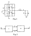
- each of two switching components connected with the power supply is in parallel connection with a capacitance and in reverse parallel connection with a diode, respectively.
- These two switching components, together with their auxiliary circuits including the power supplies, the capacitances and the diodes, constitute the up side and down side of a semi-bridge circuit, and the semi-bridge circuit is connected to the output of the converter through an inductance.
- the two switching components of the method and apparatus for digital power processing operating with zero-voltage switching can be turned off at the same time, and thus the converter is in a state with no output. It may also be such a case that one switching component is turned off while the other switching component is changed from turn-on to turn-off or vice versa. In the process of turn-on and turn-off, each of the two switching components is working in the situation that the voltages across the switching components are zero or near zero-voltage.
- This invention also provides a digital power conversion apparatus applying the zero-voltage switching digital power converter described above, comprising:
- This invention also provides a method for performing zero-voltage digital power conversion by using the digital power conversion apparatus as described above, comprising the following steps:
- two switching components T 1 and T 2 are connected to power supplies V 1 and V 2 , respectively, are in parallel connection with capacitances C 1 and C 2 and in reverse parallel connection with diodes D 1 and D 2 , respectively, and these two switching components, together with their auxiliary circuits, constitute the up side and down side of a semi-bridge circuit.
- the semi-bridge circuit connects to an inductance L connected to output terminal 3, and there is provided a capacitance C between node 3 and ground. The power can be applied to electric appliance R through terminal 3.
- the two control signals that generated by the control circuit are outputted to switching components T 1 and T 2 through terminals 1 and 2 for controlling the turn-on and turn-off status of switching components T 1 and T 2 .
- FIG. 3 shows time sequence relationship of said two control signals as described in FIG. 2.
- U T1 represents grid control voltage for T 1
- U T2 represents grid control voltage for T 2 .
- stage 1 and T 2 perform the conversion between the turn-on and turn-off status under the condition that the voltages across T1 and T2 are zero or near zero. In this way, the object of reducing the switching consumption can be achieved.
- the steps of the method for digital power conversion operating with zero-voltage switching are as follows: providing said digital power conversion apparatus; determining the discharge times based on respective parameters of C 1 , C 2 , L, C, R of the zero-voltage switching digital power converter, during which discharge times, when the turn-off status of T1 and T2 are changed to turn-on status, C 1 and C 2 connected to switching components T1 and T2 in parallel, respectively, are discharged by the inductance current of inductance L so that the voltages across C 1 and C 2 reach zero; in accordance with the above determined discharge times, configuring the control circuit to make it control the dead zone time intervals between the outputted control voltage signals U T1 and U T2 so that the dead zone time intervals are longer than or equal to corresponding discharge times, so as to guarantee that the voltage across T 1 and T 2 is kept at zero or near zero when T1 and T2 are turned on and turned off under control of said control voltages.
- switching components T1 and T2 are MOSFETs.
Landscapes
- Engineering & Computer Science (AREA)
- Power Engineering (AREA)
- Inverter Devices (AREA)
- Dc-Dc Converters (AREA)
- Analogue/Digital Conversion (AREA)
- Ac-Ac Conversion (AREA)
Applications Claiming Priority (3)
| Application Number | Priority Date | Filing Date | Title |
|---|---|---|---|
| CN01139785A CN1402416A (zh) | 2001-12-03 | 2001-12-03 | 零电压转换数字功率变换器 |
| CN01139785 | 2001-12-03 | ||
| PCT/CN2002/000863 WO2003052915A1 (fr) | 2001-12-03 | 2002-12-03 | Procede de conversion de puissance numerique et dispositif a tension nulle |
Publications (3)
| Publication Number | Publication Date |
|---|---|
| EP1478084A1 true EP1478084A1 (fr) | 2004-11-17 |
| EP1478084A4 EP1478084A4 (fr) | 2008-10-15 |
| EP1478084B1 EP1478084B1 (fr) | 2012-02-08 |
Family
ID=4675412
Family Applications (1)
| Application Number | Title | Priority Date | Filing Date |
|---|---|---|---|
| EP02782656A Expired - Lifetime EP1478084B1 (fr) | 2001-12-03 | 2002-12-03 | Procede de conversion de puissance numerique et dispositif a tension nulle |
Country Status (7)
| Country | Link |
|---|---|
| US (1) | US7215040B2 (fr) |
| EP (1) | EP1478084B1 (fr) |
| JP (2) | JP2005513985A (fr) |
| CN (1) | CN1402416A (fr) |
| AT (1) | ATE545191T1 (fr) |
| AU (1) | AU2002349471A1 (fr) |
| WO (1) | WO2003052915A1 (fr) |
Cited By (1)
| Publication number | Priority date | Publication date | Assignee | Title |
|---|---|---|---|---|
| USRE47601E1 (en) | 2013-08-19 | 2019-09-10 | Analog Devices, Inc. | High output power digital-to-analog converter system |
Families Citing this family (8)
| Publication number | Priority date | Publication date | Assignee | Title |
|---|---|---|---|---|
| WO2009027758A1 (fr) * | 2007-09-01 | 2009-03-05 | Brusa Elektronik Ag | Convertisseur de puissance de commutation à tension nulle |
| CN101355322B (zh) * | 2008-09-05 | 2011-06-15 | 南京航空航天大学 | 半周期工作的单电感双降压式半桥逆变器的控制方法 |
| EP2385617A1 (fr) | 2010-05-06 | 2011-11-09 | Brusa Elektronik AG | Commande et procédé pour un convertisseur de courant continu et convertisseur de courant continu |
| US9281788B2 (en) | 2013-03-15 | 2016-03-08 | Analog Devices, Inc. | All digital zero-voltage switching |
| US10056924B2 (en) | 2013-08-19 | 2018-08-21 | Analog Devices, Inc. | High output power digital-to-analog converter system |
| US11201562B1 (en) * | 2019-06-23 | 2021-12-14 | Purdue Research Foundation | Soft-switching voltage-edge-rate-limiting power inverter |
| CN114157137B (zh) * | 2021-10-07 | 2023-07-18 | 山西大学 | 一种内外环协作辅助换流的等效电容分压软开关逆变器 |
| CN114094804B (zh) * | 2021-10-21 | 2025-09-23 | 中山市宝辰机电设备有限公司 | 一种可控的零电压软开关电路 |
Family Cites Families (9)
| Publication number | Priority date | Publication date | Assignee | Title |
|---|---|---|---|---|
| US5666280A (en) * | 1993-05-07 | 1997-09-09 | Philips Electronics North America Corporation | High voltage integrated circuit driver for half-bridge circuit employing a jet to emulate a bootstrap diode |
| JPH0746853A (ja) * | 1993-07-29 | 1995-02-14 | Toshiba Corp | ソフトスイッチング式インバータ制御方法及びその装置 |
| CN1033121C (zh) * | 1993-08-31 | 1996-10-23 | 电子科技大学 | 恒频零电压边沿谐振开关变换器 |
| JP2677215B2 (ja) * | 1994-12-14 | 1997-11-17 | 日本電気株式会社 | ゼロボルトスイッチパルス幅変調型スイッチングレギュレータの制御回路 |
| US5594324A (en) | 1995-03-31 | 1997-01-14 | Space Systems/Loral, Inc. | Stabilized power converter having quantized duty cycle |
| US5734258A (en) * | 1996-06-03 | 1998-03-31 | General Electric Company | Bidirectional buck boost converter |
| CN1055804C (zh) | 1998-04-27 | 2000-08-23 | 深圳市华为电气股份有限公司 | 一种软开关拓扑电路 |
| JP2001258269A (ja) * | 2000-03-15 | 2001-09-21 | Kawasaki Steel Corp | ソフトスイッチングdc−dcコンバータ |
| JP2001333576A (ja) * | 2000-05-23 | 2001-11-30 | Fuji Electric Co Ltd | Dc/dcコンバータの制御方法 |
-
2001
- 2001-12-03 CN CN01139785A patent/CN1402416A/zh active Pending
-
2002
- 2002-12-03 AT AT02782656T patent/ATE545191T1/de active
- 2002-12-03 AU AU2002349471A patent/AU2002349471A1/en not_active Abandoned
- 2002-12-03 JP JP2003553698A patent/JP2005513985A/ja active Pending
- 2002-12-03 WO PCT/CN2002/000863 patent/WO2003052915A1/fr not_active Ceased
- 2002-12-03 EP EP02782656A patent/EP1478084B1/fr not_active Expired - Lifetime
- 2002-12-03 US US10/497,436 patent/US7215040B2/en not_active Expired - Lifetime
-
2009
- 2009-04-16 JP JP2009099999A patent/JP4955728B2/ja not_active Expired - Fee Related
Cited By (1)
| Publication number | Priority date | Publication date | Assignee | Title |
|---|---|---|---|---|
| USRE47601E1 (en) | 2013-08-19 | 2019-09-10 | Analog Devices, Inc. | High output power digital-to-analog converter system |
Also Published As
| Publication number | Publication date |
|---|---|
| CN1402416A (zh) | 2003-03-12 |
| US7215040B2 (en) | 2007-05-08 |
| JP2009189242A (ja) | 2009-08-20 |
| JP4955728B2 (ja) | 2012-06-20 |
| WO2003052915A1 (fr) | 2003-06-26 |
| AU2002349471A1 (en) | 2003-06-30 |
| EP1478084B1 (fr) | 2012-02-08 |
| US20040245973A1 (en) | 2004-12-09 |
| EP1478084A4 (fr) | 2008-10-15 |
| JP2005513985A (ja) | 2005-05-12 |
| ATE545191T1 (de) | 2012-02-15 |
Similar Documents
| Publication | Publication Date | Title |
|---|---|---|
| US5313382A (en) | Reduced voltage/zero current transition boost power converter | |
| US8829865B2 (en) | Power factor correction efficiency improvement circuit, a converter employing the circuit and a method of manufacturing a converter | |
| JP2961897B2 (ja) | スイッチング電源装置 | |
| JP4955728B2 (ja) | ゼロ電圧スイッチングによって動作するデジタル電力処理の方法および装置 | |
| US20020054499A1 (en) | Power conversion apparatus | |
| US20230246548A1 (en) | Switched capacitor voltage converter circuit and switched capacitor voltage conversion method | |
| CN107294385B (zh) | 用于零电压转换功率转换器的自适应定时的方法和设备 | |
| CN116111854B (zh) | 一种恒流驱动电路、恒流驱动器及恒流驱动控制方法 | |
| CN110190752B (zh) | 一种双向clllc-dcx谐振变换器及其控制方法 | |
| CN115085531A (zh) | 一种图腾柱pfc电路的控制方法、装置和电子设备 | |
| CN110994982B (zh) | 一种软开关方式的buck变换器及其控制方法 | |
| US6522109B2 (en) | Power conversion apparatus | |
| JPH0746853A (ja) | ソフトスイッチング式インバータ制御方法及びその装置 | |
| CN111628654A (zh) | 一种开关电源电路 | |
| EP3576277B1 (fr) | Procédé de commande d'un convertisseur en pont complet décalé en phase et convertisseur en pont complet décalé en phase | |
| CN110504835B (zh) | 一种开关变换器及其控制方法 | |
| JP2003134817A (ja) | 電源装置 | |
| US20090115381A1 (en) | Automatic frequency control for series resonant switched mode power supply | |
| US12483148B2 (en) | Flyback converter with high efficiency and control method thereof | |
| CN110168890B (zh) | 调节时钟驱动的变换器的具有双点调节器的控制电路 | |
| CN112165247B (zh) | 一种无桥pfc电路的零电流采样方法及其电路 | |
| US11527963B2 (en) | Control unit for improving conversion efficiency | |
| KR100401291B1 (ko) | 이중 전압 입력 전압제어 발진기를 이용한 압전 변압기의공진 구동 시스템 및 방법 | |
| CN203896213U (zh) | 用于软开关zvt变换器的自适应可调延时电路 | |
| CN101227148B (zh) | 一种有源钳位电路的错相并联运行的实现电路 |
Legal Events
| Date | Code | Title | Description |
|---|---|---|---|
| PUAI | Public reference made under article 153(3) epc to a published international application that has entered the european phase |
Free format text: ORIGINAL CODE: 0009012 |
|
| 17P | Request for examination filed |
Effective date: 20040601 |
|
| AK | Designated contracting states |
Kind code of ref document: A1 Designated state(s): AT BE BG CH CY CZ DE DK EE ES FI FR GB GR IE IT LI LU MC NL PT SE SI SK TR |
|
| AX | Request for extension of the european patent |
Extension state: AL LT LV MK RO |
|
| A4 | Supplementary search report drawn up and despatched |
Effective date: 20080911 |
|
| 17Q | First examination report despatched |
Effective date: 20090617 |
|
| REG | Reference to a national code |
Ref country code: DE Ref legal event code: R079 Ref document number: 60242184 Country of ref document: DE Free format text: PREVIOUS MAIN CLASS: H02M0007000000 Ipc: H02M0003337000 |
|
| GRAP | Despatch of communication of intention to grant a patent |
Free format text: ORIGINAL CODE: EPIDOSNIGR1 |
|
| RIC1 | Information provided on ipc code assigned before grant |
Ipc: H02M 7/538 20070101ALI20110901BHEP Ipc: H02M 3/337 20060101AFI20110901BHEP Ipc: H02M 3/155 20060101ALI20110901BHEP |
|
| GRAS | Grant fee paid |
Free format text: ORIGINAL CODE: EPIDOSNIGR3 |
|
| GRAA | (expected) grant |
Free format text: ORIGINAL CODE: 0009210 |
|
| AK | Designated contracting states |
Kind code of ref document: B1 Designated state(s): AT BE BG CH CY CZ DE DK EE ES FI FR GB GR IE IT LI LU MC NL PT SE SI SK TR |
|
| REG | Reference to a national code |
Ref country code: GB Ref legal event code: FG4D |
|
| REG | Reference to a national code |
Ref country code: AT Ref legal event code: REF Ref document number: 545191 Country of ref document: AT Kind code of ref document: T Effective date: 20120215 Ref country code: CH Ref legal event code: EP |
|
| REG | Reference to a national code |
Ref country code: DE Ref legal event code: R096 Ref document number: 60242184 Country of ref document: DE Effective date: 20120405 |
|
| REG | Reference to a national code |
Ref country code: NL Ref legal event code: VDEP Effective date: 20120208 |
|
| PG25 | Lapsed in a contracting state [announced via postgrant information from national office to epo] |
Ref country code: NL Free format text: LAPSE BECAUSE OF FAILURE TO SUBMIT A TRANSLATION OF THE DESCRIPTION OR TO PAY THE FEE WITHIN THE PRESCRIBED TIME-LIMIT Effective date: 20120208 |
|
| PG25 | Lapsed in a contracting state [announced via postgrant information from national office to epo] |
Ref country code: PT Free format text: LAPSE BECAUSE OF FAILURE TO SUBMIT A TRANSLATION OF THE DESCRIPTION OR TO PAY THE FEE WITHIN THE PRESCRIBED TIME-LIMIT Effective date: 20120608 Ref country code: FI Free format text: LAPSE BECAUSE OF FAILURE TO SUBMIT A TRANSLATION OF THE DESCRIPTION OR TO PAY THE FEE WITHIN THE PRESCRIBED TIME-LIMIT Effective date: 20120208 Ref country code: GR Free format text: LAPSE BECAUSE OF FAILURE TO SUBMIT A TRANSLATION OF THE DESCRIPTION OR TO PAY THE FEE WITHIN THE PRESCRIBED TIME-LIMIT Effective date: 20120509 Ref country code: BE Free format text: LAPSE BECAUSE OF FAILURE TO SUBMIT A TRANSLATION OF THE DESCRIPTION OR TO PAY THE FEE WITHIN THE PRESCRIBED TIME-LIMIT Effective date: 20120208 |
|
| REG | Reference to a national code |
Ref country code: AT Ref legal event code: MK05 Ref document number: 545191 Country of ref document: AT Kind code of ref document: T Effective date: 20120208 |
|
| PG25 | Lapsed in a contracting state [announced via postgrant information from national office to epo] |
Ref country code: CY Free format text: LAPSE BECAUSE OF FAILURE TO SUBMIT A TRANSLATION OF THE DESCRIPTION OR TO PAY THE FEE WITHIN THE PRESCRIBED TIME-LIMIT Effective date: 20120208 |
|
| PG25 | Lapsed in a contracting state [announced via postgrant information from national office to epo] |
Ref country code: CZ Free format text: LAPSE BECAUSE OF FAILURE TO SUBMIT A TRANSLATION OF THE DESCRIPTION OR TO PAY THE FEE WITHIN THE PRESCRIBED TIME-LIMIT Effective date: 20120208 Ref country code: DK Free format text: LAPSE BECAUSE OF FAILURE TO SUBMIT A TRANSLATION OF THE DESCRIPTION OR TO PAY THE FEE WITHIN THE PRESCRIBED TIME-LIMIT Effective date: 20120208 Ref country code: SI Free format text: LAPSE BECAUSE OF FAILURE TO SUBMIT A TRANSLATION OF THE DESCRIPTION OR TO PAY THE FEE WITHIN THE PRESCRIBED TIME-LIMIT Effective date: 20120208 Ref country code: EE Free format text: LAPSE BECAUSE OF FAILURE TO SUBMIT A TRANSLATION OF THE DESCRIPTION OR TO PAY THE FEE WITHIN THE PRESCRIBED TIME-LIMIT Effective date: 20120208 Ref country code: SE Free format text: LAPSE BECAUSE OF FAILURE TO SUBMIT A TRANSLATION OF THE DESCRIPTION OR TO PAY THE FEE WITHIN THE PRESCRIBED TIME-LIMIT Effective date: 20120208 |
|
| PG25 | Lapsed in a contracting state [announced via postgrant information from national office to epo] |
Ref country code: SK Free format text: LAPSE BECAUSE OF FAILURE TO SUBMIT A TRANSLATION OF THE DESCRIPTION OR TO PAY THE FEE WITHIN THE PRESCRIBED TIME-LIMIT Effective date: 20120208 Ref country code: IT Free format text: LAPSE BECAUSE OF FAILURE TO SUBMIT A TRANSLATION OF THE DESCRIPTION OR TO PAY THE FEE WITHIN THE PRESCRIBED TIME-LIMIT Effective date: 20120208 |
|
| PLBE | No opposition filed within time limit |
Free format text: ORIGINAL CODE: 0009261 |
|
| STAA | Information on the status of an ep patent application or granted ep patent |
Free format text: STATUS: NO OPPOSITION FILED WITHIN TIME LIMIT |
|
| 26N | No opposition filed |
Effective date: 20121109 |
|
| PG25 | Lapsed in a contracting state [announced via postgrant information from national office to epo] |
Ref country code: AT Free format text: LAPSE BECAUSE OF FAILURE TO SUBMIT A TRANSLATION OF THE DESCRIPTION OR TO PAY THE FEE WITHIN THE PRESCRIBED TIME-LIMIT Effective date: 20120208 |
|
| REG | Reference to a national code |
Ref country code: DE Ref legal event code: R097 Ref document number: 60242184 Country of ref document: DE Effective date: 20121109 |
|
| PG25 | Lapsed in a contracting state [announced via postgrant information from national office to epo] |
Ref country code: ES Free format text: LAPSE BECAUSE OF FAILURE TO SUBMIT A TRANSLATION OF THE DESCRIPTION OR TO PAY THE FEE WITHIN THE PRESCRIBED TIME-LIMIT Effective date: 20120519 |
|
| PG25 | Lapsed in a contracting state [announced via postgrant information from national office to epo] |
Ref country code: BG Free format text: LAPSE BECAUSE OF FAILURE TO SUBMIT A TRANSLATION OF THE DESCRIPTION OR TO PAY THE FEE WITHIN THE PRESCRIBED TIME-LIMIT Effective date: 20120508 Ref country code: MC Free format text: LAPSE BECAUSE OF NON-PAYMENT OF DUE FEES Effective date: 20121231 |
|
| REG | Reference to a national code |
Ref country code: CH Ref legal event code: PL |
|
| REG | Reference to a national code |
Ref country code: IE Ref legal event code: MM4A |
|
| PG25 | Lapsed in a contracting state [announced via postgrant information from national office to epo] |
Ref country code: LI Free format text: LAPSE BECAUSE OF NON-PAYMENT OF DUE FEES Effective date: 20121231 Ref country code: IE Free format text: LAPSE BECAUSE OF NON-PAYMENT OF DUE FEES Effective date: 20121203 Ref country code: CH Free format text: LAPSE BECAUSE OF NON-PAYMENT OF DUE FEES Effective date: 20121231 |
|
| PG25 | Lapsed in a contracting state [announced via postgrant information from national office to epo] |
Ref country code: TR Free format text: LAPSE BECAUSE OF FAILURE TO SUBMIT A TRANSLATION OF THE DESCRIPTION OR TO PAY THE FEE WITHIN THE PRESCRIBED TIME-LIMIT Effective date: 20120208 |
|
| PG25 | Lapsed in a contracting state [announced via postgrant information from national office to epo] |
Ref country code: LU Free format text: LAPSE BECAUSE OF NON-PAYMENT OF DUE FEES Effective date: 20121203 |
|
| PGFP | Annual fee paid to national office [announced via postgrant information from national office to epo] |
Ref country code: DE Payment date: 20141125 Year of fee payment: 13 Ref country code: GB Payment date: 20141203 Year of fee payment: 13 |
|
| PGFP | Annual fee paid to national office [announced via postgrant information from national office to epo] |
Ref country code: FR Payment date: 20141208 Year of fee payment: 13 |
|
| REG | Reference to a national code |
Ref country code: DE Ref legal event code: R119 Ref document number: 60242184 Country of ref document: DE |
|
| GBPC | Gb: european patent ceased through non-payment of renewal fee |
Effective date: 20151203 |
|
| REG | Reference to a national code |
Ref country code: FR Ref legal event code: ST Effective date: 20160831 |
|
| PG25 | Lapsed in a contracting state [announced via postgrant information from national office to epo] |
Ref country code: GB Free format text: LAPSE BECAUSE OF NON-PAYMENT OF DUE FEES Effective date: 20151203 Ref country code: DE Free format text: LAPSE BECAUSE OF NON-PAYMENT OF DUE FEES Effective date: 20160701 |
|
| PG25 | Lapsed in a contracting state [announced via postgrant information from national office to epo] |
Ref country code: FR Free format text: LAPSE BECAUSE OF NON-PAYMENT OF DUE FEES Effective date: 20151231 |