EP1478011A1 - Method and device for polishing - Google Patents
Method and device for polishing Download PDFInfo
- Publication number
- EP1478011A1 EP1478011A1 EP03705359A EP03705359A EP1478011A1 EP 1478011 A1 EP1478011 A1 EP 1478011A1 EP 03705359 A EP03705359 A EP 03705359A EP 03705359 A EP03705359 A EP 03705359A EP 1478011 A1 EP1478011 A1 EP 1478011A1
- Authority
- EP
- European Patent Office
- Prior art keywords
- polishing
- workpiece
- liquid
- active agent
- nitride film
- Prior art date
- Legal status (The legal status is an assumption and is not a legal conclusion. Google has not performed a legal analysis and makes no representation as to the accuracy of the status listed.)
- Granted
Links
Images






Classifications
-
- B—PERFORMING OPERATIONS; TRANSPORTING
- B24—GRINDING; POLISHING
- B24B—MACHINES, DEVICES, OR PROCESSES FOR GRINDING OR POLISHING; DRESSING OR CONDITIONING OF ABRADING SURFACES; FEEDING OF GRINDING, POLISHING, OR LAPPING AGENTS
- B24B53/00—Devices or means for dressing or conditioning abrasive surfaces
- B24B53/017—Devices or means for dressing, cleaning or otherwise conditioning lapping tools
-
- B—PERFORMING OPERATIONS; TRANSPORTING
- B24—GRINDING; POLISHING
- B24B—MACHINES, DEVICES, OR PROCESSES FOR GRINDING OR POLISHING; DRESSING OR CONDITIONING OF ABRADING SURFACES; FEEDING OF GRINDING, POLISHING, OR LAPPING AGENTS
- B24B37/00—Lapping machines or devices; Accessories
- B24B37/04—Lapping machines or devices; Accessories designed for working plane surfaces
-
- B—PERFORMING OPERATIONS; TRANSPORTING
- B24—GRINDING; POLISHING
- B24B—MACHINES, DEVICES, OR PROCESSES FOR GRINDING OR POLISHING; DRESSING OR CONDITIONING OF ABRADING SURFACES; FEEDING OF GRINDING, POLISHING, OR LAPPING AGENTS
- B24B37/00—Lapping machines or devices; Accessories
- B24B37/04—Lapping machines or devices; Accessories designed for working plane surfaces
- B24B37/042—Lapping machines or devices; Accessories designed for working plane surfaces operating processes therefor
- B24B37/044—Lapping machines or devices; Accessories designed for working plane surfaces operating processes therefor characterised by the composition of the lapping agent
-
- B—PERFORMING OPERATIONS; TRANSPORTING
- B24—GRINDING; POLISHING
- B24B—MACHINES, DEVICES, OR PROCESSES FOR GRINDING OR POLISHING; DRESSING OR CONDITIONING OF ABRADING SURFACES; FEEDING OF GRINDING, POLISHING, OR LAPPING AGENTS
- B24B49/00—Measuring or gauging equipment for controlling the feed movement of the grinding tool or work; Arrangements of indicating or measuring equipment, e.g. for indicating the start of the grinding operation
- B24B49/12—Measuring or gauging equipment for controlling the feed movement of the grinding tool or work; Arrangements of indicating or measuring equipment, e.g. for indicating the start of the grinding operation involving optical means
-
- B—PERFORMING OPERATIONS; TRANSPORTING
- B24—GRINDING; POLISHING
- B24B—MACHINES, DEVICES, OR PROCESSES FOR GRINDING OR POLISHING; DRESSING OR CONDITIONING OF ABRADING SURFACES; FEEDING OF GRINDING, POLISHING, OR LAPPING AGENTS
- B24B53/00—Devices or means for dressing or conditioning abrasive surfaces
- B24B53/02—Devices or means for dressing or conditioning abrasive surfaces of plane surfaces on abrasive tools
-
- B—PERFORMING OPERATIONS; TRANSPORTING
- B24—GRINDING; POLISHING
- B24B—MACHINES, DEVICES, OR PROCESSES FOR GRINDING OR POLISHING; DRESSING OR CONDITIONING OF ABRADING SURFACES; FEEDING OF GRINDING, POLISHING, OR LAPPING AGENTS
- B24B7/00—Machines or devices designed for grinding plane surfaces on work, including polishing plane glass surfaces; Accessories therefor
- B24B7/20—Machines or devices designed for grinding plane surfaces on work, including polishing plane glass surfaces; Accessories therefor characterised by a special design with respect to properties of the material of non-metallic articles to be ground
- B24B7/22—Machines or devices designed for grinding plane surfaces on work, including polishing plane glass surfaces; Accessories therefor characterised by a special design with respect to properties of the material of non-metallic articles to be ground for grinding inorganic material, e.g. stone, ceramics, porcelain
- B24B7/228—Machines or devices designed for grinding plane surfaces on work, including polishing plane glass surfaces; Accessories therefor characterised by a special design with respect to properties of the material of non-metallic articles to be ground for grinding inorganic material, e.g. stone, ceramics, porcelain for grinding thin, brittle parts, e.g. semiconductors, wafers
-
- C—CHEMISTRY; METALLURGY
- C09—DYES; PAINTS; POLISHES; NATURAL RESINS; ADHESIVES; COMPOSITIONS NOT OTHERWISE PROVIDED FOR; APPLICATIONS OF MATERIALS NOT OTHERWISE PROVIDED FOR
- C09G—POLISHING COMPOSITIONS; SKI WAXES
- C09G1/00—Polishing compositions
-
- H—ELECTRICITY
- H10—SEMICONDUCTOR DEVICES; ELECTRIC SOLID-STATE DEVICES NOT OTHERWISE PROVIDED FOR
- H10P—GENERIC PROCESSES OR APPARATUS FOR THE MANUFACTURE OR TREATMENT OF DEVICES COVERED BY CLASS H10
- H10P95/00—Generic processes or apparatus for manufacture or treatments not covered by the other groups of this subclass
- H10P95/06—Planarisation of inorganic insulating materials
- H10P95/062—Planarisation of inorganic insulating materials involving a dielectric removal step
Definitions
- the present invention relates to a polishing method and apparatus, and more particularly to a polishing method and apparatus for polishing a workpiece such as a semiconductor wafer with a fixed abrasive.
- CMP chemical mechanical polishing
- This type of chemical mechanical polishing (CMP) apparatus comprises a polishing table having a polishing pad attached thereon, and a top ring.
- a workpiece to be polished is disposed between the polishing pad and the top ring and pressed against the polishing table by the top ring, while a polishing liquid (slurry) is being supplied onto the polishing pad, and hence the workpiece is polished to a flat mirror finish.
- a polishing liquid slurry
- FIGS. 3A through 3F are schematic cross-sectional views showing an example of the STI forming process.
- a nitride film 110 (generally, a film of silicon nitride Si 3 N 4 ) is formed on a silicon substrate 100 (see FIG. 3A), and the silicon substrate 100 is etched using the nitride film 110 as a mask, thus forming a trench (groove) 120 (see FIG. 3B).
- a silicon oxide film 130 made of an insulating material is embedded in the trench 120 (see FIG. 3C).
- the excessive layer of the silicon oxide film 130 is removed by CMP, thereby exposing the surface of the nitride film 110 (see FIG. 3D). Then, the nitride film 110 is etched away, thus forming a groove 130a of the silicon oxide film (see FIG. 3E). A transistor 140 is then formed using such groove 130a of the silicon oxide film (see FIG. 3F).
- the purpose of the polishing step using CMP is to completely remove the excessive silicon oxide film formed on the nitride film. If the excessive silicon oxide film is not removed completely, then the subsequent etching of the nitride film will be impaired.
- the polishing step in the above-mentioned conventional STI forming process employs a polyurethane-based polishing pad and a slurry with silica abrasive particles dispersed therein. Since the nitride film 110 is less liable to be polished than the silicon oxide film 130, the silicon oxide film 130 is excessively polished, thus developing dishing as shown in FIG. 4. Furthermore, the nitride film tends to be polished unevenly, resulting in insufficient within-wafer uniformity.
- the STI forming process it is necessary to strictly control the thicknesses of the nitride film and the silicon oxide film in the trench, i.e., to uniformize the film thickness within the surface of the wafer, and it is important to suppress dishing for within-wafer uniformity.
- the purpose of this process is to increase the polishing rate by making the pH alkaline to sufficiently increase the dispersion of dropped abrasive particles.
- the publication refers to nothing about optimization of the polishing process which includes multi-stage polishing, dressing, and post-processing.
- the present invention has been made in view of the above problems in the prior art. It is therefore an object of the present invention to provide a polishing method and a polishing apparatus which can suppress dishing in a workpiece having a nitride film and an oxide film formed on the nitride film, and obtain within-wafer uniformity.
- a polishing method for polishing a workpiece by pressing the workpiece to be polished against a fixed abrasive and bringing the workpiece in sliding contact with the fixed abrasive characterized in that while supplying a polishing liquid which contains an anionic or cationic surface-active agent and does not contain abrasive particles, the workpiece is polished.
- a polishing method for polishing a workpiece by pressing the workpiece to be polished against a polishing surface and bringing the workpiece in sliding contact with the polishing surface comprising: a first step of polishing the workpiece while supplying a polishing liquid which contains an anionic surface-active agent; and a second step of polishing the workpiece while supplying a polishing liquid which contains a cationic surface-active agent.
- the cationic surface-active agent should preferably contain at least one organic compound having any one structure of aliphatic amine salt, aliphatic quaternary ammonium salt, benzalkonium salt, benzethonium chloride, pyridinium salt, or imidazolium salt.
- the concentration of the anionic surface-active agent in the polishing liquid is preferably 0.001 % by weight to 5 % by weight, and the pH of the polishing liquid is preferably 5 to 10.
- the anionic surface-active agent preferably contains an organic compound having a hydrophilic group selected from COO - group and SO 3 - group.
- the workpiece preferably has a nitride film and a silicon oxide film deposited on the nitride film.
- the surfaces of the abrasive particles of the fixed abrasive and the surface of the nitride film are principally charged positively (though part of the surfaces possess a negative charge, a positive charge is predominant). Accordingly, the anionic surface-active agent supplied onto the fixed abrasive strongly adheres to the surfaces of the abrasive particles of the fixed abrasive and to the surface of the nitride film electrically. Since the abrasive particles of the fixed abrasive and the nitride film are both covered with the anionic surface-active agent to interact repulsively.
- polishing of the nitride film is hard to proceed and the polishing rate of the nitride film becomes extremely low.
- the nitride film is not polished and only the silicon oxide film is polished, and the above-described dishing will proceed. In fact, however, dishing does not proceed, and depth of the dishing amount can be controlled, for example, within 100 ⁇ or less. This is considered to be due to the following reasons:
- the present invention uses a fixed abrasive as a polishing surface.
- a fixed abrasive provides a hard polishing surface which hardly deforms elastically. Such a polishing surface, as compared to a conventional polishing pad having elasticity, is less likely to cause dishing and can provide a flatter finished surface.
- the polishing pad, a slurry, and a surface-active agent may be used.
- polishing of a workpiece is carried out while supplying the polishing liquid which contains an anionic surface-active agent and does not contain abrasive particles, onto the fixed abrasive, whereby a nitride film, for example, is allowed to act as a polishing stopper.
- the polishing method of the present invention can lower the polishing rate of a nitride film to obtain within-wafer uniformity of the nitride film and can suppress dishing, thus enabling a high-flatness polishing with fewer scratches.
- FIG. 1 is a plan view showing a whole arrangement of a polishing apparatus according to an embodiment of the present invention.
- the polishing apparatus comprises four load/unload stages 2 each for receiving a wafer cassette 1 which accommodates a number of semiconductor wafers.
- the load/unload stages 2 may have a lifting and lowering mechanism.
- a transfer robot 4 is provided on rails 3 so that the transfer robot 4 can access the respective wafer cassettes 1 on the respective load/unload stages 2.
- the transfer robot 4 has upper and lower hands.
- the lower hand of the transfer robot 4 is a vacuum attraction-type hand for holding a semiconductor wafer under vacuum, and is used only for removing a semiconductor wafer from a wafer cassette 1.
- the vacuum attraction-type hand can hold and transport the semiconductor wafer even if the semiconductor wafer is not located at a normal position in the wafer cassette due to a slight displacement.
- the upper hand of the transfer robot 4 is a recess support-type hand for supporting a peripheral edge of a wafer, and is used only for returning the semiconductor wafer to the wafer cassette 1.
- the recess support-type hand can transport the semiconductor wafer while keeping the semiconductor wafer clean because dust is not collected, unlike the vacuum attraction-type hand. In this manner, since a clean wafer which has been cleaned is held by the upper hand, the clean semiconductor wafer is not further contaminated.
- Two cleaning units 5, 6 for cleaning a semiconductor wafer are disposed at an opposite side of the wafer cassettes 1 with respect to the rails 3 of the transfer robot 4.
- the cleaning units 5, 6 are disposed at positions accessible by the hands of the transfer robot 4.
- Each of the cleaning units 5, 6 has a spin-dry mechanism for drying a wafer by spinning the wafer at a high speed, and hence two-stage cleaning and three-stage cleaning of a wafer can be performed without replacing any cleaning module.
- a wafer station 12 having four semiconductor wafer supports 7, 8, 9 and 10 is disposed at a position accessible by the transfer robot 4.
- a transfer robot 14 having two hands is disposed at a position where hands of the transfer robot 14 can access the cleaning unit 5 and the three supports 7, 9 and 10.
- a transfer robot 15 having two hands is disposed at a position where hands of the transfer robot 15 can access the cleaning unit 6 and the three supports 8, 9 and 10.
- the support 7 is used to transfer a semiconductor wafer between the transfer robot 4 and the transfer robot 14, and the support 8 is used to transfer a semiconductor wafer between the transfer robot 4 and the transfer robot 15.
- These supports 7, 8 have sensors 16, 17 for detecting existence of a semiconductor wafer, respectively.
- the support 9 is used to transfer a semiconductor wafer from the transfer robot 15 to the transfer robot 14, and the support 10 is used to transfer a semiconductor wafer from the transfer robot 14 to the transfer robot 15.
- These supports 9, 10 have sensors 18, 19 for detecting existence of a semiconductor wafer, and rinsing nozzles 20, 21 for preventing the semiconductor wafer from being dried or rinsing the wafer.
- the supports 9 and 10 are disposed in a common water-scatter-prevention cover which has an opening defined therein for transferring wafers therethrough. At the opening, there is provided a shutter 22.
- the support 9 is disposed above the support 10.
- the upper support 9 serves to support a wafer which has been cleaned, and the lower support 10 serves to support a wafer to be cleaned. With this arrangement, the wafer is prevented from being contaminated by rinsing liquid which would otherwise fall thereon.
- the sensors 16, 17, 18 and 19, the rinsing nozzles 20, 21, and the shutter 22 are schematically shown in FIG. 1, and their positions and shapes are not exactly illustrated.
- a cleaning unit 24 is disposed at a position adjacent to the cleaning unit 5 and is accessible by the hands of the transfer robot 14. Further, a cleaning unit 25 is disposed at a position adjacent to the cleaning unit 6 and is accessible by hands of the transfer robot 15. These cleaning units 24 and 25 are capable of cleaning both surfaces of a wafer.
- the respective upper hands of the transfer robot 14 and the transfer robot 15 are used for transporting a semiconductor wafer that has been cleaned to the cleaning units or the supports of the wafer station 12.
- the respective lower hands of the transfer robot 14 and the transfer robot 15 are used for transporting a semiconductor wafer that has not cleaned or a semiconductor wafer to be polished. Since the lower hands are used to transfer a wafer to or from a reversing device (described later on), the upper hands are not contaminated by drops of rinsing liquid which fall from an upper wall of the reversing device.
- the cleaning units 5, 6, 24 and 25 have shutters 5a, 6a, 24a and 25a at respective wafer entrances for transferring wafers therethrough, respectively.
- the shutters 5a, 6a, 24a and 25a are opened only when wafers are transferred through the shutters 5a, 6a, 24a and 25a.
- the polishing apparatus has a housing 26 for enclosing various components therein.
- An interior of the housing 26 is partitioned into a plurality of areas (including areas A and B) by partition walls 28, 30, 32, 34 and 36.
- the partition wall 28 has an opening for transferring semiconductor wafers between area A and area B, and a shutter 38 is provided at the opening of the partition wall 28. All of the cleaning units 5, 6, 24 and 25, the supports 7, 8, 9 and 10 of the wafer station 12, and the transfer robots 14 and 15 are placed in area B. Pressure in area B is adjusted so as to be lower than pressure in area A.
- a reversing device 40 for reversing a semiconductor wafer is provided at a position accessible by the hands of the transfer robot 14.
- the semiconductor wafer is transferred to the reversing device 40 by the transfer robot 14.
- a reversing device 41 for reversing a semiconductor wafer is provided at a position accessible by the hands of the transfer robot 15.
- the semiconductor wafer is transferred to the reversing device 41 by the transfer robot 15.
- Each of the reversing devices 40 and 41 has a chuck mechanism for chucking a semiconductor wafer, a reversing mechanism for reversing the semiconductor wafer, and a detecting sensor for detecting whether or not the chuck mechanism chucks the semiconductor wafer.
- the partition wall 34 forms a polishing chamber which is separated from area B.
- the polishing chamber is further divided into two areas C and D by the partition wall 36.
- the partition wall 34 between area B and areas C, D has openings for transferring semiconductor wafers therethrough.
- Shutters 42, 43 for the reversing devices 40, 41 are respectively provided at the openings of the partition wall 34.
- each of areas C and D has two polishing tables and one top ring for holding and pressing one semiconductor wafer against the polishing tables to polish the wafer.
- area C has a top ring 44, polishing tables 46, 48, a polishing liquid supply nozzle 50 for supplying a polishing liquid onto the polishing table 46, an atomizer 52 having a plurality of ejection nozzles (not shown) connected to a nitrogen gas supply source and a liquid supply source, a dresser 54 for dressing the polishing table 46, and a dresser 56 for dressing the polishing table 48.
- area D has a top ring 45, polishing tables 47, 49, a polishing liquid supply nozzle 51 for supplying a polishing liquid onto the polishing table 47, an atomizer 53 having a plurality of ejection nozzles (not shown) connected to a nitrogen gas supply source and a liquid supply source, a dresser 55 for dressing the polishing table 47, and a dresser 57 for dressing the polishing table 49.
- the polishing tables 48, 49 have, for example, Politex pads (Rodel) for buffing cleaning attached thereto, and have liquid supply nozzles 58-2, 59-2.
- the polishing liquid supply nozzles 50, 51, 58-1, 59-1 supply polishing liquids, used for a polishing process, and dressing liquids (e.g., water) used for a dressing process, onto the polishing tables 46, 47, respectively.
- the atomizers 52, 53 eject liquids composed of a mixture of nitrogen gas with pure water or a chemical liquid onto the polishing tables 46, 47, respectively. Nitrogen gas from the nitrogen gas supply source and pure water or a chemical liquid from the liquid supply source are passed through a regulator or air operated valve (not shown) to regulate pressure thereof to a predetermined value, and supplied to the ejection nozzles in the atomizers 52, 53 in a mixed state.
- the liquid should preferably be ejected from the ejection nozzles of the atomizers 52, 53 toward outer peripheral edges of the polishing tables 46, 47.
- Other inert gases may be used instead of nitrogen gas.
- the atomizers 52, 53 may eject only a liquid of pure water or a chemical liquid.
- the polishing tables 48, 49 may have atomizers as with the polishing tables 46, 47, respectively. With atomizers for the polishing tables 48, 49, surfaces of the polishing tables 48, 49 can be kept clean.
- the mixture of nitrogen gas with pure water or the chemical liquid is supplied in a state of 1 ⁇ liquid fine particles, 2 ⁇ solid fine particles as a result of solidification of the liquid, or 3 ⁇ gas as a result of vaporization of the liquid.
- These states 1 ⁇ , 2 ⁇ and 3 ⁇ are referred to as atomization.
- the mixture is ejected from the ejection nozzles of the atomizers 52, 53 toward the polishing tables 46, 47.
- pressure or temperature of the nitrogen gas and/or the pure water or the chemical liquid, or the shape of the nozzles determines which state of the mixed liquid is to be ejected, i.e., the liquid fine particles, the solid fine particles, or gas.
- the state of the liquid to be ejected can be varied, for example, by properly adjusting pressure or temperature of the nitrogen gas and/or the pure water or the chemical liquid with use of a regulator or the like, or by properly adjusting the shape of the nozzles.
- the polishing tables 48, 49 may be replaced with wet-type thickness measuring devices for measuring a thickness of a film formed on a wafer.
- wet-type thickness measuring devices for measuring a thickness of a film formed on a wafer.
- the thickness of a film formed on a wafer can be measured immediately after the wafer is polished, and hence it is possible to further polish 'the polished wafer or to control a polishing process for polishing a subsequent wafer based on measured results.
- a rotary transporter 60 is disposed below the reversing devices 40 and 41 and the top rings 44 and 45 to transfer wafers between the cleaning chamber (area B) and the polishing chamber (areas C, D).
- the rotary transporter 60 has four stages for placing wafers W at equal angular intervals, and can hold a plurality of wafers thereon at the same time.
- a wafer which has been transferred to the reversing device 40 or 41 is transferred to the rotary transporter 60 by elevating and lowering a lifter 62 or 63 disposed below the rotary transporter 60 when a center of a stage of the rotary transporter 60 is aligned with a center of the wafer held by the reversing device 40 or 41.
- a wafer placed on the stage of the rotary transporter 60 is transported to a position below the top ring 44 or the top ring 45 by rotating the rotary transporter 60 by an angle of 90°.
- the top ring 44 or the top ring 45 is positioned above the rotary transporter 60 beforehand by a swinging motion of the top ring.
- a wafer held on the stage of the rotary transporter 60 is transferred to the top ring 44 or 45 by elevating and lowering a pusher 64 or 65 disposed below the rotary transporter 60 when a center of the top ring 44 or 45 is aligned with a center of the wafer.
- FIG. 2 shows a relationship between the top ring 44 and the polishing tables 46, 48 in area C.
- the top ring 44 is supported from a top ring head 72 by a top ring drive shaft 70 which is rotatable.
- the top ring head 72 is supported by a support shaft 74 which can angularly be positioned, and the top ring 44 can access the polishing tables 46 and 48.
- the dresser 54 is supported from a dresser head 78 by a dresser drive shaft 76 which is rotatable.
- the dresser head 78 is supported by a support shaft 80 which can angularly be positioned, and the dresser 54 can be moved between a standby position and a dressing position above the polishing table 46.
- the dresser 56 is similarly supported from a dresser head 84 by a dresser drive shaft 82 which is rotatable.
- the dresser head 84 is supported by a support shaft 86 which can angularly be positioned, and the dresser 56 can be moved between a standby position and a dressing position above the polishing table 48.
- the dresser comprises one of a diamond dresser with diamond particles fixed to a metal or ceramic plate, a nylon brush, a ceramic plate with surface irregularities, a carbon fiber brush, a fixed abrasive material, a waterjet stream, a cavitation jet stream, an ultrasonic oscillator, ultraviolet rays, and a laser beam, or a combination of them.
- the polishing table 46 has an upper surface composed of a fixed abrasive 46a having abrasive particles and pores or a pore agent, which are fixed by a binder (resin).
- the fixed abrasive 46a serves as a polishing surface for polishing a semiconductor wafer held by the top ring 44.
- Such a fixed abrasive 46a can be obtained, for example, by spray-drying a mixed liquid which is a mixture of a slurry of abrasive (dispersion of abrasive particles in a liquid) and a resin emulsion, filling the resulting mixed powder into a molding jig, and subjecting the mixed powder to a pressure/heat treatment.
- Ceria (CeO 2 ) or silica (SiO 2 ) having an average particle diameter of not more than 0.5 ⁇ m is preferably used as the abrasive particles.
- a thermoplastic resin or a thermosetting resin may be used as the binder. The thermoplastic resin is preferably used.
- the polishing table 48 has an upper surface composed of a soft nonwoven fabric.
- the nonwoven fabric serves as a cleaning surface for cleaning a semiconductor wafer after a polishing process to remove abrasive particles attached to a surface of the semiconductor wafer.
- a polishing process for polishing a semiconductor wafer with the use of a polishing apparatus according to the present invention will be described below.
- a polishing process only in area C will be described below, the following description can be applied to a polishing process in area D.
- the present invention is also applicable, for example, to polishing of a semiconductor wafer having a pattern of interlayer dielectrics (ILD).
- ILD interlayer dielectrics
- a silicon oxide film in a trench tends to develop dishing because a nitride film can be reached by polishing in a short period of time.
- an ex-situ dressing process (described below) is employed.
- the polishing table 46 and the dresser 54 are rotated about their own axes, respectively, and the dresser 54 is pressed against the polishing table 46 to dress the fixed abrasive 46a.
- the atomizer 52 ejects a mixture of DIW (pure water) and nitrogen gas to the fixed abrasive 46a.
- polishing table 46 and the top ring 44 are rotated about their own axes, respectively, a semiconductor wafer is pressed against the polishing table 46 to thereby polish a silicon oxide film on the semiconductor wafer until the fixed abrasive reaches a nitride film.
- a polishing liquid which contains an anionic surface-active agent and does not contain abrasive particles is supplied from the polishing liquid supply nozzle 50 onto the fixed abrasive 46a.
- concentration of the anionic surface-active agent is preferably 0.001 % by weight to 5 % by weight.
- the pH of the polishing liquid is preferably in the range of from 5 to 10.
- the anionic surface-active agent preferably contains an organic compound having a hydrophilic group which is either a COO - group or a SO 3 - group.
- the polishing table 46 and the top ring 44 are rotated about their own axes, respectively, and the semiconductor wafer is pressed against the polishing table 46 for water-polishing.
- the polishing liquid supply nozzle 50 supplies a polishing liquid or DIW to the fixed abrasive 46a.
- the pressing force applied to the wafer in this process is smaller than the pressing force applied to the wafer in the preceding polishing process.
- the polishing table 46, the dresser 54, and the top ring 44 are rotated about their own axes, respectively, and the semiconductor wafer is polished while the fixed abrasive 46a is being dressed.
- the polishing liquid supply nozzle 50 supplies pure water or an alkaline liquid to the fixed abrasive 46a, and the atomizer 52 ejects a mixture of DIW and nitrogen gas to the fixed abrasive 46a.
- the dresser 54 stops dressing the fixed abrasive 46a, and the semiconductor wafer is continuously polished.
- the polishing liquid supply nozzle 50 supplies a polishing liquid which contains an anionic surface-active agent and does not contain abrasive particles.
- the semiconductor wafer is polished, while the fixed abrasive 46a is being dressed, up to a time immediately before the nitride film on the semiconductor wafer is reached (until the remaining thickness of the silicon oxide film on the nitride film becomes about 1000 ⁇ ) (in-situ dressing).
- dressing of the fixed abrasive is stopped, and the semiconductor wafer is continuously polished until the nitride film is reached.
- the nitride film acts as a polishing stopper, as described above. Therefore, the polishing rate of the nitride film is lowered to achieve within-wafer uniformity on the nitride film and also to prevent dishing.
- the semiconductor wafer is thus polished for high planarity with few scratches thereon.
- the polishing table 46 and the top ring 44 are rotated about their own axes, respectively, and the semiconductor wafer is pressed against the polishing table 46 for water-polishing.
- the polishing liquid supply nozzle 50 supplies a polishing liquid or DIW to the fixed abrasive 46a.
- the pressing force applied to the wafer in this process is smaller than the pressing force applied to the wafer in the preceding polishing process.
- the semiconductor wafer is polished while a polishing liquid which contains an anionic surface-active agent and does not contain abrasive particles is being supplied to the fixed abrasive 46a, and the nitride film acts as a polishing stopper. If the nitride film needs to be polished, then the semiconductor wafer may continuously be polished while a polishing liquid which contains a cationic surface-active agent and does not contain abrasive particles is being supplied to the fixed abrasive 46a.
- the cationic surface-active agent should preferably comprise at least one organic compound having any one structure of aliphatic amine salt, aliphatic quaternary ammonium salt, benzalkonium salt, benzethonium chloride, pyridinium salt, or imidazolium salt.
- the polishing selectivity (the ratio between the polishing rates of the nitride film and the oxide film) of the polishing liquid which contains the anionic surface-active agent is increased at the time when the nitride film and the oxide film are simultaneously exposed on the surface being polished, it is effective to add the polishing liquid according to the present invention at the latter stage of the polishing process.
- the polishing liquid may be switched to the polishing liquid which contains the anionic surface-active agent at, or immediately prior to, the time when part of the nitride film starts being exposed. Before that time (while only the oxide film is being polished), the semiconductor wafer is polished while a polishing liquid containing a low concentration anionic surface-active agent or pure water is being supplied.
- the polishing process according to the present invention which employs the fixed abrasive has better planarizing characteristics than the conventional CMP process, and requirements for improving the planarizing characteristics in the STI forming process and the metal gate forming process are very high.
- FIG. 5 shows a polishing sequence in which a fixed abrasive polishing process is applied to an STI forming process.
- the purpose for polishing an STI forming wafer is to remove a silicon oxide film 130 covering a silicon nitride film 110 to expose the silicon nitride film 110 (first and second polishing steps).
- the polishing process is finished when the silicon nitride film is exposed.
- the polishing process may be continued until the silicon nitride film 110 is polished to a predetermined film thickness (third polishing step).
- the goal to be achieved at the time when the second polishing step is finished is to suppress dishing of a trench 120 to minimize irregularities of the remaining film thickness of the silicon nitride film 110. If the polishing is performed using pure water, then dishing of the silicon oxide film 130 in the trench 120 progresses, and the silicon nitride film 110 is gradually polished, resulting in increased irregularities of the remaining film thickness thereof. In order to suppress such dishing, the second polishing step is performed while a polishing liquid containing an anionic surface-active agent that is diluted to a predetermined concentration is being supplied. If such a polishing liquid is used, then the silicon nitride film 110 is not substantially polished, and hence serves as a stopper for stopping the polishing process. Therefore, irregularities of the remaining film thickness of the silicon nitride film 110 can be suppressed to a low level. For the reasons described above, dishing of the silicon oxide film 130 in the trench 120 can also be reduced.
- the polishing rate of the silicon oxide film 130 is also lowered. If the silicon oxide film 130 is polished while a polishing liquid containing an anionic surface-active agent that is diluted to a predetermined concentration is being supplied from the beginning of the first polishing step, then since the polishing time is increased, the productivity is lowered. In the first polishing step, only the silicon oxide film 130 is polished (the silicon nitride film 110 is not polished), it is basically unnecessary to add the polishing liquid containing the anionic surface-active agent.
- the anionic surface-active agent is added, then even though the anionic surface-active agent is of a low concentration, the anionic surface-active agent is deposited in concavities of the non-flat surface (uneven surface) of the silicon oxide film 130 and protects the concavities from polishing, thus improving planarizing characteristics.
- the anionic surface-active agent is also effective to increase the dispersion of the abrasive particles which contribute to the polishing process.
- the anionic surface-active agent of a low concentration does not essentially lower the polishing rate of the silicon oxide film 130.
- the polishing rate is lowered and the polishing time is correspondingly increased. Therefore, it is desirable to shorten the polishing time in the first polishing step as much as possible. Consequently, it is preferable in the first polishing step to supply the polishing liquid whose concentration of the anionic surface-active agent is as low as possible (at least lower than the concentration used in the second polishing step), to polish the silicon oxide film 130 at an increased polishing rate, and to polish the silicon oxide film 130 down to a position as close to the silicon nitride film 110 as possible.
- the first polishing step is switched to the second polishing step on the basis of time, or by detecting a table torque current change or detecting the remaining film thickness of the silicon oxide film 130.
- the goal to be achieved by the first polishing step should preferably be at least a planarized surface, or more preferably be the remaining film thickness of the silicon oxide film 130 smaller than 100 nm or preferably 50 nm.
- the endpoint of each of the polishing steps is detected by one of a process of detecting a processing endpoint based on a change in the torque current of a table drive motor for the polishing table, a process of applying light to the wafer and detecting the intensity of reflected light to read a change in the film thickness of the silicon oxide film 130 or the silicon nitride film 110, and a process of applying light to the wafer and reading a change in the optical reflectance of the material of the surface being polished to detect the endpoint, or a combination of them.
- the silicon nitride film 110 may be polished by adding a certain cationic surface-active agent that has been adjusted to a predetermined concentration.
- a cationic surface-active agent is added, though the overall polishing rate is relatively low, the silicon oxide film 130 and the silicon nitride film 110 can be polished at substantially the same polishing rate. Since the polishing rate is low, the silicon nitride film 110 can be polished while reducing film thickness variations thereof. Since the polishing rates of the silicon oxide film 130 and the silicon nitride film 110 are approximately the same as each other, the silicon oxide film 130 is prevented from being excessively polished, i.e., from developing dishing.
- the process of polishing an STI wafer may be finished in the second polishing step.
- the third polishing step is required if the CMP process is applied to a gate forming process, for example, as shown in FIG. 6.
- the silicon nitride film 110 and the silicon oxide film 130 need to be polished simultaneously because the silicon nitride film 110 directly above the gate has to be completely removed to expose the lower layer. Therefore, it is necessary to perform the entire polishing process through the first and second polishing steps until the final third polishing step.
- the three steps may be carried out on a single polishing table or may be carried out on respective tables.
- the polishing liquid may be supplied from respective polishing liquid supply nozzles in the respective three steps or may be supplied from a single polishing liquid supply nozzle in the three steps.
- the first and second steps may be carried out on a single polishing table or may be carried out on respective tables. If the polishing process needs to be performed up to the third step, then the second and third steps should preferably be performed on respective tables for the reason that different surface-active agents are used in these steps.
- the first polishing step it is preferable in the first polishing step to increase the polishing rate (so as to be faster than at least the polishing rate in the second step) by the necessity of shortening a polishing time.
- the concentration of the anionic surface-active agent that is contained in the polishing liquid used in the first polishing step should preferably be lower than the concentration of the anionic surface-active agent used in the second polishing step.
- the polishing liquid may be pure water.
- the degree of dressing may be heighten by increasing the dressing time, increasing the pressing force of the dresser, applying light at an increased intensity, or increasing irradiation time of light.
- the polishing rate may be lowered if the relative speed is increased to a certain value or more.
- the dressing (conditioning) mechanism is not limited to the illustrated mechanism, but may be any of various other means.
- the polishing abrasive particles used for polishing is supplied from the fixed abrasive (pad) itself.
- the abrasive particles are generally liberated from the fixed abrasive (pad) itself due to a load applied in the polishing process or sliding friction caused in the polishing process. If the liberation of the abrasive particles is weak, then the fixed abrasive surface is dressed (conditioned) to promote the liberation of the abrasive particles.
- Abrasive particles that are thus separated from the fixed abrasive include larger particles that are loosely joined into agglomerates or are firmly joined into agglomerates. These larger particles are a major factor in damaging the wafer surface.
- a pressurized fluid comprising a mixture of a gas and a liquid to the surface of the fixed abrasive during or after the dressing.
- the gas used in the atomizer should preferably be an inert gas such as a nitrogen gas.
- the liquid used in the atomizer may usually be pure water, but may be a chemical liquid containing an anionic surface-active agent for the purpose of dispersing agglomerated abrasive particles made up of abrasive particles that are loosely joined together.
- These means should preferably be used in the first polishing step, but may also be used in the second or third polishing step.
- the liquid used in the second polishing step may comprise an anionic surface-active agent adjusted to a predetermined concentration
- the liquid used in the third polishing step may comprise a cationic surface-active agent adjusted to a predetermined concentration.
- the semiconductor wafer which has thus been polished by the fixed abrasive 46a in the in-situ or ex-situ dressing process is moved to the smaller-diameter table 48, on which the semiconductor wafer is subjected to buff cleaning.
- the polished semiconductor wafer held by the top ring 44 is pressed against a soft non-woven cloth on the polishing table 48.
- the non-woven cloth is supplied with an abrasive-free liquid, e.g., pure water or an alkaline liquid, preferably an alkaline liquid of pH 9 or higher or an alkaline liquid containing TMAH, from the cleaning liquid supply nozzle 58-2.
- an abrasive-free liquid e.g., pure water or an alkaline liquid, preferably an alkaline liquid of pH 9 or higher or an alkaline liquid containing TMAH
- the semiconductor wafer may be cleaned with DHF by the cleaning unit 24 or 25.
- abrasive particles attached to the surface of the polished semiconductor wafer may effectively be removed by cleaning the wafer surface with a roll brush while diluted hydrofluoric acid (DHF) is being added. Since diluted hydrofluoric acid (DHF) acts to etch the silicon oxide film 130 on the wafer surface, it can completely remove the abrasive particles attached to the wafer surface together with the silicon oxide film 130 therebeneath.
- DHF diluted hydrofluoric acid
- the surface of the semiconductor wafer may be cleaned by, for example, a pen-shaped sponge member.
- a finish-polishing of the semiconductor wafer may be performed after the semiconductor wafer has been polished by the fixed abrasive 46a.
- the finish-polishing of the semiconductor wafer may be performed on the polishing table 46 or the polishing table 48. In either case, the finish-polishing of the semiconductor wafer is performed using a polishing liquid containing abrasive particles, and after the finish-polishing, the above water-polishing process and the cleaning process (buff cleaning or DHF cleaning) are performed.
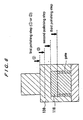
- FIGS. 7A and 7B are views showing a polishing apparatus according to another embodiment of the present invention, FIG. 7A being a plan view of a polishing table of the polishing apparatus and FIG. 7B being a cross-sectional view of the polishing apparatus.
- the polishing apparatus has an optical sensor 230 disposed in the polishing table 46.
- the optical sensor 230 comprises a light-emitting element and a light-detecting element.
- the light-emitting element applies light to the surface, being polished, of the semiconductor wafer, and the light-detecting element detects light reflected from the surface being polished.
- the light emitted from the light-emitting element comprises either a laser beam or an LED light beam.
- the silicon oxide film or the silicon nitride film is polished to a predetermined film thickness
- part of the light applied from the light-emitting element to the surface, being polished, of the semiconductor wafer passes through the film, and is reflected from a film beneath the film being polished. Therefore, there are two types of light reflected from the semiconductor wafer, i.e., the light reflected from the film beneath the film being polished, and the light reflected from the surface of the film being polished.
- the light-detecting element detects the two types of reflected light, and outputs a signal to a controller 232.
- the controller 232 processes the supplied signal to accurately detect the film thickness of the remaining silicon oxide film or silicon nitride film.
- polishing liquid supply apparatus and a polishing apparatus having such polishing liquid supply apparatus according to the present invention will be described below.
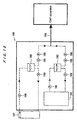
- FIG. 8 is a view showing a concentration adjusting facility 160 disposed outside of a CMP apparatus.
- the polishing liquid supply apparatus has a raw liquid container 161 which contains a surface-active agent having a predetermined concentration.
- the surface-active agent is diluted for use.
- the surface-active agent is diluted near or within the polishing apparatus, so that the raw liquid container 161 may be small in size.
- the raw liquid container 161 supplies the raw liquid to concentration adjustment containers 164, 166 respectively by pumps 162, 163 having a flow rate adjusting function.
- the concentration adjustment containers 164, 166 are supplied with pure water at flow rates adjusted respectively by flow rate controllers 168, 169 for achieving predetermined surface-active agent concentrations, respectively.
- an anionic surface-active agent which is of a very low concentration is used in the first polishing step and an anionic surface-active agent which is of a concentration higher than that in the first polishing step is used in the second polishing step, then two surface-active agents having different concentrations can be prepared from the raw liquid supplied from the common raw liquid container 161 as in the present embodiment.
- the surface-active agents thus prepared are supplied through respective lines 1, 2 to the CMP apparatus.
- the surface-active agents may be supplied to the CMP apparatus through a single supply line having a selector valve.
- FIG. 9 is a view showing a concentration adjusting facility 160 disposed within a CMP apparatus.
- a surface-active agent concentration adjusting mechanism is disposed within the CMP apparatus.
- the surface-active agent concentration adjusting mechanism shown in FIG. 9 is identical to that shown in FIG. 8, and will not be described in detail below.
- FIG. 10 is a view showing a concentration adjusting facility 180 disposed outside of a CMP apparatus.
- a raw liquid container 181 is connected to a mixing pipe 193 through a pump 182 for drawing a raw liquid from the raw liquid container 181, a raw liquid buffer container 183, a circulation line valve 184, a discharge valve 185, and a pump 186 having a discharge flow rate adjusting function.
- a pure water supply line has a pure water supply source 187, a valve 188, a pure water buffer container 189, a circulation line valve 190, a discharge valve 191, and a pump 192 having a discharge flow rate adjusting function, and is connected to the mixing pipe 193.
- the raw liquid buffer container 183 and the pure water buffer container 189 are capable of keeping a flow rate and a pressure of the liquid in the mixing pipe 193 constant to adjust a surface-active agent to a desired concentration even when the pressure in the raw liquid container changes and the pressure in the pure water supply source 187 is high.
- FIG. 11 is a view showing a concentration adjusting facility disposed within a CMP apparatus.
- the concentration adjusting facility shown in FIG. 11 is identical to the concentration adjusting facility shown in FIG. 10, and will not be described in detail below.
- FIG. 12 is a view showing an example of layout of a raw liquid solution 181 and a pure water supply source 187 disposed outside of a CMP apparatus, and other equipment disposed within the CMP apparatus. Other structural details shown in FIG. 12 are identical to those shown in FIGS. 10 and 11.
- polishing liquid concentration adjusting mechanisms are provided.
- a pure water supply source for supplying a diluent may be shared by the polishing liquid concentration adjusting mechanisms.
- polishing of a workpiece is carried out while supplying the polishing liquid which contains an anionic surface-active agent and does not contain abrasive particles, onto the fixed abrasive, whereby a nitride film, for example, is allowed to act as a polishing stopper.
- the polishing method of the present invention can lower the polishing rate of a nitride film to obtain within-wafer uniformity of the nitride film and can suppress dishing, thus enabling a high-flatness polishing with fewer scratches.
- the present invention is preferably applicable to a polishing method and apparatus for polishing a workpiece such as a semiconductor wafer using a fixed abrasive.
Landscapes
- Engineering & Computer Science (AREA)
- Mechanical Engineering (AREA)
- Chemical & Material Sciences (AREA)
- Ceramic Engineering (AREA)
- Inorganic Chemistry (AREA)
- Organic Chemistry (AREA)
- Mechanical Treatment Of Semiconductor (AREA)
- Finish Polishing, Edge Sharpening, And Grinding By Specific Grinding Devices (AREA)
- Grinding-Machine Dressing And Accessory Apparatuses (AREA)
Abstract
Description
Claims (28)
- A polishing method for polishing a workpiece by pressing the workpiece to be polished against a fixed abrasive and bringing the workpiece in sliding contact with the fixed abrasive, comprising:a first step of polishing the workpiece while supplying a polishing liquid which contains an anionic surface-active agent and does not contain abrasive particles; anda second step of polishing the workpiece while supplying a polishing liquid which contains a cationic surface-active agent and does not contain abrasive particles.
- A polishing method for polishing a workpiece by pressing the workpiece to be polished against a polishing surface and bringing the workpiece in sliding contact with the polishing surface, comprising:a first step of polishing the workpiece while supplying a polishing liquid which contains an anionic surface-active agent; anda second step of polishing the workpiece while supplying a polishing liquid which contains a cationic surface-active agent.
- A polishing method according to claim 1 or 2, wherein said cationic surface-active agent contains at least one organic compound having any one structure of aliphatic amine salt, aliphatic quaternary ammonium salt, benzalkonium salt, benzethonium chloride, pyridinium salt, or imidazolium salt.
- A polishing method according to claim 1 or 2, wherein said anionic surface-active agent contains an organic compound having a hydrophilic group selected from COO- group and SO3 - group.
- A polishing method according to any one of claims 1 to 4, wherein said workpiece has a nitride film and a silicon oxide film deposited on the nitride film.
- A polishing method for polishing a workpiece having an upper layer composed of a silicon oxide film and a lower layer composed partly of a silicon nitride film by pressing the workpiece against a polishing surface and bringing the workpiece in sliding contact with the polishing surface, said upper layer being non-flat, comprising:a first polishing step of polishing the workpiece while supplying a first polishing liquid which contains an anionic surface-active agent or pure water until said upper layer is planarized over the entire surface of the workpiece; anda second polishing step of polishing the workpiece while supplying a second polishing liquid which contains an anionic surface-active agent until the silicon oxide film formed on the silicon nitride film of the lower layer is removed to expose the substantially entire surface of the silicon nitride film.
- A polishing method according to claim 6, wherein said polishing surface comprises a fixed abrasive, and said polishing liquids do not contain abrasive particles.
- A polishing method according to claim 6 or 7, wherein in said first polishing step, the workpiece is polished until the silicon oxide film formed on the silicon nitride film of the lower layer has a film thickness of 100 nm or less.
- A polishing method according to claim 6 or 7, wherein in said first polishing step, the workpiece is polished until the silicon oxide film formed on the silicon nitride film of the lower layer has a film thickness of 50 nm or less.
- A polishing method according to any one of claims 6 to 9, further comprising a third polishing step of polishing said silicon nitride film to a predetermined film thickness while supplying a third polishing liquid which contains a cationic surface-active agent and does not contain abrasive particles, after said second polishing step.
- A polishing method according to any one of claims 6 to 10, wherein at least one of said polishing steps is performed on at least one polishing table.
- A polishing method according to any one of claims 6 to 11, wherein the anionic surface-active agent in the polishing liquid used in said first polishing step has a concentration lower than the anionic surface-active agent used in said second polishing step.
- A polishing method according to claim 10, wherein said cationic surface-active agent in the polishing liquid contains at least one organic compound having any one structure of aliphatic amine salt, aliphatic quaternary ammonium salt, benzalkonium salt, benzethonium chloride, pyridinium salt, or imidazolium salt.
- A polishing method according to any one of claims 6 to 13, wherein a polishing rate of said first polishing step is higher than a polishing rate of said second polishing step.
- A polishing method according to claim 14, wherein a means for increasing the polishing rate of said first polishing step comprises at least one of making a surface pressure of the workpiece higher than that in said second polishing step, making a polishing relative speed higher than that in said second polishing step, or dressing the polishing surface by a dressing intensity higher than that in said second polishing step.
- A polishing method according to claim 15, wherein a means for dressing the polishing surface comprises at least one of a dresser with diamond particles fixed to a metal or ceramic plate, a nylon brush, a ceramic plate with surface irregularities, a carbon fiber brush, a fixed abrasive, a waterjet stream, a cavitation jet stream, an ultrasonic oscillator, ultraviolet rays, and a laser beam.
- A polishing method according to any one of claims 6 to 16, wherein in at least one of said polishing steps, a pressurized fluid comprising a mixture of a gas and a liquid is ejected to the polishing surface, said liquid comprising pure water or a surface-active agent.
- A polishing method according to any one of claims 6 to 17, further comprising cleaning the workpiece by pressing the workpiece against a non-fixed-abrasive pad and bringing the workpiece in sliding contact with the non-fixed-abrasive pad while supplying pure water or a chemical liquid which does not contain abrasive particles, after said second or third polishing step.
- A polishing method according to any one of claims 6 to 17, further comprising cleaning the workpiece while supplying diluted hydrofluoric acid (DHF), after said second or third polishing step.
- A polishing method according to any one of claims 6 to 17, wherein in at least one of said polishing steps, a polishing endpoint is detected by using at least one of a process of reading a change in a torque current of a table drive motor for a table having the polishing surface, a process of reading a change in the film thickness of the silicon oxide film on the surface of the workpiece, and a process of reading a change in the optical reflectance of a material.
- A polishing apparatus comprising:a fixed abrasive;a top ring for pressing a workpiece to be polished against said fixed abrasive;a polishing liquid supply means for supplying at least two types of polishing liquids containing surface-active agents, respectively, to said fixed abrasive; andat least one dressing means for dressing a surface of said fixed abrasive.
- A polishing apparatus according to claim 21, further comprising a facility for adjusting said polishing liquids to predetermined concentrations.
- A polishing apparatus according to claim 22, wherein said concentration adjusting facility is disposed separately outside of said polishing apparatus, and said concentration adjusting facility has at least two polishing liquid concentration adjusting containers and at least two polishing liquid supply pipes for supplying the polishing liquids whose concentrations have been adjusted to said polishing apparatus.
- A polishing apparatus according to claim 22, wherein said concentration adjusting facility is disposed within said polishing apparatus, and said concentration adjusting facility has at least two polishing liquid concentration adjusting containers and at least two polishing liquid supply pipes for supplying the polishing liquids whose concentrations have been adjusted to a polishing unit.
- A polishing apparatus according to claim 22, wherein the concentrations of said polishing liquids are adjusted outside of said polishing apparatus or within said polishing apparatus;
said polishing apparatus further comprising:a means for adjusting a flow rate of a polishing raw liquid in a polishing raw liquid supply pipe;a means for adjusting a flow rate of pure water in a pure water supply pipe;a means for introducing the polishing raw liquid with the adjusted flow rate and the pure water with the adjusted flow rate into a mixing pipe and adjusting the concentrations of the polishing liquids in said mixing pipe; anda means for supplying the polishing liquids with the adjusted concentrations to a polishing unit. - A polishing apparatus according to claim 21, further comprising a buff cleaning table for performing buff cleaning on the polished workpiece.
- A polishing apparatus according to claim 21, further comprising a diluted hydrofluoric acid (DHF) supply facility for cleaning the polished workpiece with diluted hydrofluoric acid.
- A polishing apparatus according to claim 21, further comprising at least one of an endpoint detecting device having a detector for detecting a change in a torque current of a table drive motor for a table having the polishing surface and a processor for processing a detected signal from said detector to detect an endpoint, an endpoint detecting device having a detector for detecting a change in the film thickness of a silicon oxide film or a silicon nitride film on the surface of the workpiece and a processor for processing a detected signal from said detector to detect an endpoint, and an endpoint detecting device having a detector for detecting a change in the optical reflectance of a material and a processor for processing a detected signal from said detector to detect an endpoint.
Applications Claiming Priority (3)
| Application Number | Priority Date | Filing Date | Title |
|---|---|---|---|
| JP2002043471 | 2002-02-20 | ||
| JP2002043471 | 2002-02-20 | ||
| PCT/JP2003/001869 WO2003071592A1 (en) | 2002-02-20 | 2003-02-20 | Method and device for polishing |
Publications (3)
| Publication Number | Publication Date |
|---|---|
| EP1478011A1 true EP1478011A1 (en) | 2004-11-17 |
| EP1478011A4 EP1478011A4 (en) | 2005-06-01 |
| EP1478011B1 EP1478011B1 (en) | 2008-04-09 |
Family
ID=27750526
Family Applications (2)
| Application Number | Title | Priority Date | Filing Date |
|---|---|---|---|
| EP03705360A Expired - Lifetime EP1478012B1 (en) | 2002-02-20 | 2003-02-20 | Polishing method and polishing fluid |
| EP03705359A Expired - Lifetime EP1478011B1 (en) | 2002-02-20 | 2003-02-20 | Method and device for polishing |
Family Applications Before (1)
| Application Number | Title | Priority Date | Filing Date |
|---|---|---|---|
| EP03705360A Expired - Lifetime EP1478012B1 (en) | 2002-02-20 | 2003-02-20 | Polishing method and polishing fluid |
Country Status (6)
| Country | Link |
|---|---|
| US (2) | US20040248415A1 (en) |
| EP (2) | EP1478012B1 (en) |
| JP (2) | JPWO2003071592A1 (en) |
| CN (2) | CN100369210C (en) |
| DE (2) | DE60315257T2 (en) |
| WO (2) | WO2003071593A1 (en) |
Families Citing this family (40)
| Publication number | Priority date | Publication date | Assignee | Title |
|---|---|---|---|---|
| KR20040031071A (en) * | 2001-09-28 | 2004-04-09 | 신에쯔 한도타이 가부시키가이샤 | Grinding work holding disk, work grinding device and grinding method |
| US20050287932A1 (en) * | 2004-06-25 | 2005-12-29 | Basol Bulent M | Article for polishin substrate surface |
| ITMI20041788A1 (en) * | 2004-09-20 | 2004-12-20 | St Microelectronics Srl | "MULTI-STATION ROTARY MACHINE FOR THE SANDING OF WAFER OF SEMICONDUCTOR ELECTRONIC COMPONENTS" |
| US20060097219A1 (en) * | 2004-11-08 | 2006-05-11 | Applied Materials, Inc. | High selectivity slurry compositions for chemical mechanical polishing |
| KR100640965B1 (en) * | 2004-12-30 | 2006-11-02 | 동부일렉트로닉스 주식회사 | Method of forming a semiconductor device |
| JP2006261261A (en) * | 2005-03-16 | 2006-09-28 | Renesas Technology Corp | Apparatus and method for chemical mechanical polishing |
| US20070032176A1 (en) * | 2005-08-04 | 2007-02-08 | Chih-Ming Hsu | Method for polishing diamond wafers |
| US7393789B2 (en) | 2005-09-01 | 2008-07-01 | Micron Technology, Inc. | Protective coating for planarization |
| WO2008097627A1 (en) * | 2007-02-07 | 2008-08-14 | Tbw Industries, Inc. | Cleaning cup system for chemical mechanical planarization apparatus |
| US7923373B2 (en) | 2007-06-04 | 2011-04-12 | Micron Technology, Inc. | Pitch multiplication using self-assembling materials |
| US8096852B2 (en) * | 2008-08-07 | 2012-01-17 | Applied Materials, Inc. | In-situ performance prediction of pad conditioning disk by closed loop torque monitoring |
| US8506661B2 (en) * | 2008-10-24 | 2013-08-13 | Air Products & Chemicals, Inc. | Polishing slurry for copper films |
| DE102008053610B4 (en) * | 2008-10-29 | 2011-03-31 | Siltronic Ag | Method for polishing both sides of a semiconductor wafer |
| JP5533884B2 (en) * | 2009-12-01 | 2014-06-25 | 株式会社Sumco | Wafer polishing method |
| JP5761943B2 (en) * | 2010-03-25 | 2015-08-12 | 株式会社東京精密 | Finish grinding apparatus and finish grinding method |
| KR101849797B1 (en) * | 2010-04-27 | 2018-04-17 | 쓰리엠 이노베이티브 프로퍼티즈 컴파니 | Ceramic shaped abrasive particles, methods of making the same, and abrasive articles containing the same |
| US8602838B2 (en) * | 2010-08-26 | 2013-12-10 | Mcronix International Co., Ltd. | Chemical mechanical polishing method and system |
| CN102528646A (en) * | 2010-12-31 | 2012-07-04 | 中芯国际集成电路制造(上海)有限公司 | Semiconductor grinding method |
| US8211775B1 (en) | 2011-03-09 | 2012-07-03 | United Microelectronics Corp. | Method of making transistor having metal gate |
| US8519487B2 (en) | 2011-03-21 | 2013-08-27 | United Microelectronics Corp. | Semiconductor device |
| KR102202331B1 (en) * | 2014-10-03 | 2021-01-13 | 가부시키가이샤 에바라 세이사꾸쇼 | Substrate processing apparatus and processing method |
| CN105619965A (en) * | 2014-11-28 | 2016-06-01 | 苏州力合光电薄膜科技有限公司 | Self lubricating film structure, and manufacturing method and application thereof |
| CN104493683B (en) * | 2014-11-28 | 2017-10-03 | 上海华力微电子有限公司 | A kind of method for determining thin-film grinding speed |
| CN104669075B (en) * | 2014-12-08 | 2017-08-04 | 沈阳工业大学 | Photocatalytic assisted sharpening method and device for diamond tools |
| JP6489973B2 (en) * | 2015-07-30 | 2019-03-27 | 株式会社ディスコ | Grinding equipment |
| JP2017064899A (en) * | 2015-10-01 | 2017-04-06 | 株式会社荏原製作所 | Polishing device |
| US9534148B1 (en) | 2015-12-21 | 2017-01-03 | Rohm And Haas Electronic Materials Cmp Holdings, Inc. | Method of polishing semiconductor substrate |
| JP7023455B2 (en) * | 2017-01-23 | 2022-02-22 | 不二越機械工業株式会社 | Work polishing method and work polishing equipment |
| CN107846656B (en) * | 2017-12-22 | 2024-01-12 | 镇江贝斯特新材料股份有限公司 | Polishing device for automatic flexible production line of receivers |
| US10967480B2 (en) * | 2018-10-29 | 2021-04-06 | Taiwan Semiconductor Manufacturing Company Ltd. | Apparatus and methods for chemical mechanical polishing |
| JP7316785B2 (en) | 2018-12-26 | 2023-07-28 | 株式会社荏原製作所 | How to clean the optical film thickness measurement system |
| CN110039405B (en) * | 2019-03-20 | 2024-01-05 | 广东工业大学 | Pressurized atomizing spray device, polishing device and polishing method |
| JP6698921B1 (en) * | 2019-06-30 | 2020-05-27 | 株式会社西村ケミテック | Polishing liquid supply device |
| CN110517951B (en) * | 2019-08-29 | 2022-11-29 | 上海华力集成电路制造有限公司 | Cleaning method for improving micro-scratch of wafer before STI (shallow trench isolation) grinding |
| US12285837B2 (en) | 2021-11-18 | 2025-04-29 | SanDisk Technologies, Inc. | Wafer surface chemical distribution sensing system and methods for operating the same |
| EP4250341A1 (en) * | 2022-03-24 | 2023-09-27 | Siltronic AG | Method for cleaning semiconductor disks in a cleaning line |
| US20240408650A1 (en) * | 2023-06-06 | 2024-12-12 | Applied Materials, Inc. | Method and apparatus to clean substrate with atomizing nozzle |
| CN119159506A (en) * | 2024-10-22 | 2024-12-20 | 北京晶亦精微科技股份有限公司 | A wafer photoelectrochemical mechanical polishing device, method and controller |
| CN119238229B (en) * | 2024-12-06 | 2025-02-18 | 浙江工业大学 | A photorheological polishing liquid reflux jet polishing device and polishing method thereof |
| CN119347635B (en) * | 2024-12-25 | 2025-03-28 | 常州臻晶半导体有限公司 | Silicon carbide wafer thickness measurement control device and measurement method |
Family Cites Families (32)
| Publication number | Priority date | Publication date | Assignee | Title |
|---|---|---|---|---|
| US5445996A (en) * | 1992-05-26 | 1995-08-29 | Kabushiki Kaisha Toshiba | Method for planarizing a semiconductor device having a amorphous layer |
| CN1197542A (en) * | 1995-09-13 | 1998-10-28 | 株式会社日立制作所 | Polishing methods and equipment |
| JP2000315665A (en) | 1999-04-29 | 2000-11-14 | Ebara Corp | Polishing method and apparatus |
| US6200201B1 (en) * | 1996-08-29 | 2001-03-13 | Lam Research Corporation | Cleaning/buffer apparatus for use in a wafer processing device |
| US5972792A (en) * | 1996-10-18 | 1999-10-26 | Micron Technology, Inc. | Method for chemical-mechanical planarization of a substrate on a fixed-abrasive polishing pad |
| US5990012A (en) * | 1998-01-27 | 1999-11-23 | Micron Technology, Inc. | Chemical-mechanical polishing of hydrophobic materials by use of incorporated-particle polishing pads |
| WO1999064527A1 (en) * | 1998-06-10 | 1999-12-16 | Rodel Holdings, Inc. | Composition and method for polishing in metal cmp |
| JP2000109816A (en) * | 1998-10-05 | 2000-04-18 | Okamoto Machine Tool Works Ltd | Method for preparing abrasive slurry |
| JP4095731B2 (en) * | 1998-11-09 | 2008-06-04 | 株式会社ルネサステクノロジ | Semiconductor device manufacturing method and semiconductor device |
| JP2000160136A (en) * | 1998-11-30 | 2000-06-13 | Hitachi Chem Co Ltd | Polishing agent and polishing process using the same |
| JP3728950B2 (en) * | 1998-12-04 | 2005-12-21 | 株式会社日立製作所 | Semiconductor device manufacturing method and planarization apparatus |
| US6066028A (en) * | 1998-12-14 | 2000-05-23 | The United States Of America As Represented By The Secretary Of The Navy | Polishing of copper |
| KR100754103B1 (en) * | 1998-12-25 | 2007-08-31 | 히다치 가세고교 가부시끼가이샤 | CPM abrasive, additive solution for CPM abrasive, and substrate polishing method |
| JP2000237952A (en) * | 1999-02-19 | 2000-09-05 | Hitachi Ltd | Polishing apparatus and method of manufacturing semiconductor device |
| KR20010039590A (en) * | 1999-04-29 | 2001-05-15 | 마에다 시게루 | Method and apparatus for polishing workpieces |
| DE60032423T2 (en) * | 1999-08-18 | 2007-10-11 | Ebara Corp. | Method and device for polishing |
| JP4090186B2 (en) | 1999-08-18 | 2008-05-28 | 株式会社荏原製作所 | Polishing method and polishing apparatus |
| JP2001057352A (en) * | 1999-08-18 | 2001-02-27 | Hitachi Chem Co Ltd | Method of polishing substrate |
| US6429133B1 (en) * | 1999-08-31 | 2002-08-06 | Micron Technology, Inc. | Composition compatible with aluminum planarization and methods therefore |
| US6294470B1 (en) * | 1999-12-22 | 2001-09-25 | International Business Machines Corporation | Slurry-less chemical-mechanical polishing |
| EP1272311A1 (en) * | 2000-04-07 | 2003-01-08 | Cabot Microelectronics Corporation | Integrated chemical-mechanical polishing |
| JP2001351888A (en) * | 2000-06-05 | 2001-12-21 | Okamoto Machine Tool Works Ltd | Method of detecting polishing end point of device wafer |
| US6443811B1 (en) * | 2000-06-20 | 2002-09-03 | Infineon Technologies Ag | Ceria slurry solution for improved defect control of silicon dioxide chemical-mechanical polishing |
| JP3775176B2 (en) | 2000-06-29 | 2006-05-17 | 株式会社Sumco | Semiconductor wafer manufacturing method and manufacturing apparatus |
| US6653242B1 (en) * | 2000-06-30 | 2003-11-25 | Applied Materials, Inc. | Solution to metal re-deposition during substrate planarization |
| JP2002043256A (en) * | 2000-07-27 | 2002-02-08 | Hitachi Ltd | Semiconductor wafer flattening method and flattening device |
| TW483094B (en) * | 2000-08-17 | 2002-04-11 | Macronix Int Co Ltd | Method to reduce micro-particle adsorption in semiconductor manufacturing process |
| KR20030022105A (en) * | 2001-02-20 | 2003-03-15 | 가부시키 가이샤 에바라 세이사꾸쇼 | Polishing apparatus and dressing method |
| JP2002324771A (en) | 2001-02-20 | 2002-11-08 | Ebara Corp | Polishing apparatus and dressing method |
| JP2002324772A (en) * | 2001-04-25 | 2002-11-08 | Hitachi Ltd | Semiconductor device manufacturing method and manufacturing apparatus |
| US6485355B1 (en) * | 2001-06-22 | 2002-11-26 | International Business Machines Corporation | Method to increase removal rate of oxide using fixed-abrasive |
| JP2003017447A (en) * | 2001-06-28 | 2003-01-17 | Hitachi Chem Co Ltd | Cmp abrasives and method for polishing substrate |
-
2003
- 2003-02-20 EP EP03705360A patent/EP1478012B1/en not_active Expired - Lifetime
- 2003-02-20 WO PCT/JP2003/001870 patent/WO2003071593A1/en not_active Ceased
- 2003-02-20 WO PCT/JP2003/001869 patent/WO2003071592A1/en not_active Ceased
- 2003-02-20 JP JP2003570394A patent/JPWO2003071592A1/en active Pending
- 2003-02-20 US US10/485,349 patent/US20040248415A1/en not_active Abandoned
- 2003-02-20 CN CNB038007290A patent/CN100369210C/en not_active Expired - Fee Related
- 2003-02-20 DE DE60315257T patent/DE60315257T2/en not_active Expired - Fee Related
- 2003-02-20 JP JP2003570395A patent/JPWO2003071593A1/en not_active Ceased
- 2003-02-20 EP EP03705359A patent/EP1478011B1/en not_active Expired - Lifetime
- 2003-02-20 US US10/485,273 patent/US7108579B2/en not_active Expired - Fee Related
- 2003-02-20 CN CNB038007096A patent/CN100347827C/en not_active Expired - Fee Related
- 2003-02-20 DE DE60320227T patent/DE60320227T2/en not_active Expired - Fee Related
Also Published As
| Publication number | Publication date |
|---|---|
| US20040248415A1 (en) | 2004-12-09 |
| JPWO2003071593A1 (en) | 2005-06-16 |
| DE60315257D1 (en) | 2007-09-13 |
| WO2003071592A1 (en) | 2003-08-28 |
| WO2003071593A1 (en) | 2003-08-28 |
| JPWO2003071592A1 (en) | 2005-06-16 |
| DE60320227D1 (en) | 2008-05-21 |
| EP1478012B1 (en) | 2007-08-01 |
| CN1537324A (en) | 2004-10-13 |
| EP1478012A1 (en) | 2004-11-17 |
| CN1533595A (en) | 2004-09-29 |
| CN100369210C (en) | 2008-02-13 |
| US7108579B2 (en) | 2006-09-19 |
| EP1478012A4 (en) | 2005-06-01 |
| CN100347827C (en) | 2007-11-07 |
| DE60315257T2 (en) | 2008-04-17 |
| US20040235301A1 (en) | 2004-11-25 |
| DE60320227T2 (en) | 2009-05-20 |
| EP1478011A4 (en) | 2005-06-01 |
| EP1478011B1 (en) | 2008-04-09 |
Similar Documents
| Publication | Publication Date | Title |
|---|---|---|
| US7108579B2 (en) | Method and device for polishing | |
| US6869337B2 (en) | System and method for polishing and planarizing semiconductor wafers using reduced surface area polishing pads and variable partial pad-wafer overlapping techniques | |
| JP4838614B2 (en) | Semiconductor substrate planarization apparatus and planarization method | |
| US6752692B2 (en) | Cleaning method and polishing apparatus employing such cleaning method | |
| EP0999012B1 (en) | Method and apparatus for polishing substrate | |
| US6398627B1 (en) | Slurry dispenser having multiple adjustable nozzles | |
| US20020023715A1 (en) | Substrate polishing apparatus and substrate polishing mehod | |
| TWI436853B (en) | Method and device for polishing object | |
| JP2009285738A (en) | Flattening device and flattening method for semiconductor substrate | |
| US6827633B2 (en) | Polishing method | |
| JP2003311593A (en) | Polishing apparatus | |
| US6686284B2 (en) | Chemical mechanical polisher equipped with chilled retaining ring and method of using | |
| US20020187731A1 (en) | In-situ pad and wafer cleaning during chemical mechanical polishing | |
| US6626741B2 (en) | Method for improving thickness uniformity on a semiconductor wafer during chemical mechanical polishing | |
| JP2003251555A (en) | Polishing method | |
| JP2003260663A (en) | Polishing apparatus and method | |
| JPH08250457A (en) | Vertical wafer polishing device |
Legal Events
| Date | Code | Title | Description |
|---|---|---|---|
| PUAI | Public reference made under article 153(3) epc to a published international application that has entered the european phase |
Free format text: ORIGINAL CODE: 0009012 |
|
| 17P | Request for examination filed |
Effective date: 20040129 |
|
| AK | Designated contracting states |
Kind code of ref document: A1 Designated state(s): AT BE BG CH CY CZ DE DK EE ES FI FR GB GR HU IE IT LI LU MC NL PT SE SI SK TR |
|
| A4 | Supplementary search report drawn up and despatched |
Effective date: 20050418 |
|
| RIC1 | Information provided on ipc code assigned before grant |
Ipc: 7B 24B 53/02 B Ipc: 7B 24B 37/04 B Ipc: 7B 24B 7/22 B Ipc: 7C 09K 3/14 B Ipc: 7B 24B 37/00 B Ipc: 7H 01L 21/304 A |
|
| 17Q | First examination report despatched |
Effective date: 20060201 |
|
| GRAP | Despatch of communication of intention to grant a patent |
Free format text: ORIGINAL CODE: EPIDOSNIGR1 |
|
| RBV | Designated contracting states (corrected) |
Designated state(s): DE FR |
|
| RIN1 | Information on inventor provided before grant (corrected) |
Inventor name: SASAKI, TATSUYA,EBARA CORPORATION Inventor name: AKATSUKA, TOMOHIKO,EBARA CORPORATION Inventor name: WADA, YUTAKA,EBARA CORPORATION |
|
| GRAC | Information related to communication of intention to grant a patent modified |
Free format text: ORIGINAL CODE: EPIDOSCIGR1 |
|
| GRAS | Grant fee paid |
Free format text: ORIGINAL CODE: EPIDOSNIGR3 |
|
| GRAA | (expected) grant |
Free format text: ORIGINAL CODE: 0009210 |
|
| AK | Designated contracting states |
Kind code of ref document: B1 Designated state(s): DE FR |
|
| REF | Corresponds to: |
Ref document number: 60320227 Country of ref document: DE Date of ref document: 20080521 Kind code of ref document: P |
|
| ET | Fr: translation filed | ||
| PLBE | No opposition filed within time limit |
Free format text: ORIGINAL CODE: 0009261 |
|
| STAA | Information on the status of an ep patent application or granted ep patent |
Free format text: STATUS: NO OPPOSITION FILED WITHIN TIME LIMIT |
|
| 26N | No opposition filed |
Effective date: 20090112 |
|
| PGFP | Annual fee paid to national office [announced via postgrant information from national office to epo] |
Ref country code: DE Payment date: 20090225 Year of fee payment: 7 |
|
| PGFP | Annual fee paid to national office [announced via postgrant information from national office to epo] |
Ref country code: FR Payment date: 20090128 Year of fee payment: 7 |
|
| REG | Reference to a national code |
Ref country code: FR Ref legal event code: ST Effective date: 20101029 |
|
| PG25 | Lapsed in a contracting state [announced via postgrant information from national office to epo] |
Ref country code: FR Free format text: LAPSE BECAUSE OF NON-PAYMENT OF DUE FEES Effective date: 20100301 |
|
| PG25 | Lapsed in a contracting state [announced via postgrant information from national office to epo] |
Ref country code: DE Free format text: LAPSE BECAUSE OF NON-PAYMENT OF DUE FEES Effective date: 20100901 |