EP0999012B1 - Method and apparatus for polishing substrate - Google Patents
Method and apparatus for polishing substrate Download PDFInfo
- Publication number
- EP0999012B1 EP0999012B1 EP99122248A EP99122248A EP0999012B1 EP 0999012 B1 EP0999012 B1 EP 0999012B1 EP 99122248 A EP99122248 A EP 99122248A EP 99122248 A EP99122248 A EP 99122248A EP 0999012 B1 EP0999012 B1 EP 0999012B1
- Authority
- EP
- European Patent Office
- Prior art keywords
- polishing
- cleaning
- semiconductor substrate
- substrate
- unit
- Prior art date
- Legal status (The legal status is an assumption and is not a legal conclusion. Google has not performed a legal analysis and makes no representation as to the accuracy of the status listed.)
- Expired - Lifetime
Links
Images


Classifications
-
- H—ELECTRICITY
- H01—ELECTRIC ELEMENTS
- H01L—SEMICONDUCTOR DEVICES NOT COVERED BY CLASS H10
- H01L21/00—Processes or apparatus adapted for the manufacture or treatment of semiconductor or solid state devices or of parts thereof
- H01L21/02—Manufacture or treatment of semiconductor devices or of parts thereof
- H01L21/04—Manufacture or treatment of semiconductor devices or of parts thereof the devices having at least one potential-jump barrier or surface barrier, e.g. PN junction, depletion layer or carrier concentration layer
- H01L21/18—Manufacture or treatment of semiconductor devices or of parts thereof the devices having at least one potential-jump barrier or surface barrier, e.g. PN junction, depletion layer or carrier concentration layer the devices having semiconductor bodies comprising elements of Group IV of the Periodic System or AIIIBV compounds with or without impurities, e.g. doping materials
- H01L21/30—Treatment of semiconductor bodies using processes or apparatus not provided for in groups H01L21/20 - H01L21/26
- H01L21/302—Treatment of semiconductor bodies using processes or apparatus not provided for in groups H01L21/20 - H01L21/26 to change their surface-physical characteristics or shape, e.g. etching, polishing, cutting
- H01L21/304—Mechanical treatment, e.g. grinding, polishing, cutting
-
- B—PERFORMING OPERATIONS; TRANSPORTING
- B24—GRINDING; POLISHING
- B24B—MACHINES, DEVICES, OR PROCESSES FOR GRINDING OR POLISHING; DRESSING OR CONDITIONING OF ABRADING SURFACES; FEEDING OF GRINDING, POLISHING, OR LAPPING AGENTS
- B24B37/00—Lapping machines or devices; Accessories
- B24B37/34—Accessories
- B24B37/345—Feeding, loading or unloading work specially adapted to lapping
-
- B—PERFORMING OPERATIONS; TRANSPORTING
- B24—GRINDING; POLISHING
- B24B—MACHINES, DEVICES, OR PROCESSES FOR GRINDING OR POLISHING; DRESSING OR CONDITIONING OF ABRADING SURFACES; FEEDING OF GRINDING, POLISHING, OR LAPPING AGENTS
- B24B51/00—Arrangements for automatic control of a series of individual steps in grinding a workpiece
-
- H—ELECTRICITY
- H01—ELECTRIC ELEMENTS
- H01L—SEMICONDUCTOR DEVICES NOT COVERED BY CLASS H10
- H01L21/00—Processes or apparatus adapted for the manufacture or treatment of semiconductor or solid state devices or of parts thereof
- H01L21/02—Manufacture or treatment of semiconductor devices or of parts thereof
- H01L21/02041—Cleaning
- H01L21/02057—Cleaning during device manufacture
-
- H—ELECTRICITY
- H01—ELECTRIC ELEMENTS
- H01L—SEMICONDUCTOR DEVICES NOT COVERED BY CLASS H10
- H01L21/00—Processes or apparatus adapted for the manufacture or treatment of semiconductor or solid state devices or of parts thereof
- H01L21/67—Apparatus specially adapted for handling semiconductor or electric solid state devices during manufacture or treatment thereof; Apparatus specially adapted for handling wafers during manufacture or treatment of semiconductor or electric solid state devices or components ; Apparatus not specifically provided for elsewhere
- H01L21/67005—Apparatus not specifically provided for elsewhere
- H01L21/67011—Apparatus for manufacture or treatment
- H01L21/67017—Apparatus for fluid treatment
- H01L21/67028—Apparatus for fluid treatment for cleaning followed by drying, rinsing, stripping, blasting or the like
- H01L21/6704—Apparatus for fluid treatment for cleaning followed by drying, rinsing, stripping, blasting or the like for wet cleaning or washing
- H01L21/67046—Apparatus for fluid treatment for cleaning followed by drying, rinsing, stripping, blasting or the like for wet cleaning or washing using mainly scrubbing means, e.g. brushes
-
- H—ELECTRICITY
- H01—ELECTRIC ELEMENTS
- H01L—SEMICONDUCTOR DEVICES NOT COVERED BY CLASS H10
- H01L21/00—Processes or apparatus adapted for the manufacture or treatment of semiconductor or solid state devices or of parts thereof
- H01L21/67—Apparatus specially adapted for handling semiconductor or electric solid state devices during manufacture or treatment thereof; Apparatus specially adapted for handling wafers during manufacture or treatment of semiconductor or electric solid state devices or components ; Apparatus not specifically provided for elsewhere
- H01L21/67005—Apparatus not specifically provided for elsewhere
- H01L21/67011—Apparatus for manufacture or treatment
- H01L21/67017—Apparatus for fluid treatment
- H01L21/67028—Apparatus for fluid treatment for cleaning followed by drying, rinsing, stripping, blasting or the like
- H01L21/6704—Apparatus for fluid treatment for cleaning followed by drying, rinsing, stripping, blasting or the like for wet cleaning or washing
- H01L21/67051—Apparatus for fluid treatment for cleaning followed by drying, rinsing, stripping, blasting or the like for wet cleaning or washing using mainly spraying means, e.g. nozzles
-
- H—ELECTRICITY
- H01—ELECTRIC ELEMENTS
- H01L—SEMICONDUCTOR DEVICES NOT COVERED BY CLASS H10
- H01L21/00—Processes or apparatus adapted for the manufacture or treatment of semiconductor or solid state devices or of parts thereof
- H01L21/67—Apparatus specially adapted for handling semiconductor or electric solid state devices during manufacture or treatment thereof; Apparatus specially adapted for handling wafers during manufacture or treatment of semiconductor or electric solid state devices or components ; Apparatus not specifically provided for elsewhere
- H01L21/67005—Apparatus not specifically provided for elsewhere
- H01L21/67011—Apparatus for manufacture or treatment
- H01L21/67155—Apparatus for manufacturing or treating in a plurality of work-stations
- H01L21/67207—Apparatus for manufacturing or treating in a plurality of work-stations comprising a chamber adapted to a particular process
- H01L21/67219—Apparatus for manufacturing or treating in a plurality of work-stations comprising a chamber adapted to a particular process comprising at least one polishing chamber
-
- H—ELECTRICITY
- H01—ELECTRIC ELEMENTS
- H01L—SEMICONDUCTOR DEVICES NOT COVERED BY CLASS H10
- H01L21/00—Processes or apparatus adapted for the manufacture or treatment of semiconductor or solid state devices or of parts thereof
- H01L21/02—Manufacture or treatment of semiconductor devices or of parts thereof
- H01L21/02041—Cleaning
- H01L21/02043—Cleaning before device manufacture, i.e. Begin-Of-Line process
- H01L21/02052—Wet cleaning only
-
- H—ELECTRICITY
- H01—ELECTRIC ELEMENTS
- H01L—SEMICONDUCTOR DEVICES NOT COVERED BY CLASS H10
- H01L21/00—Processes or apparatus adapted for the manufacture or treatment of semiconductor or solid state devices or of parts thereof
- H01L21/02—Manufacture or treatment of semiconductor devices or of parts thereof
- H01L21/04—Manufacture or treatment of semiconductor devices or of parts thereof the devices having at least one potential-jump barrier or surface barrier, e.g. PN junction, depletion layer or carrier concentration layer
- H01L21/18—Manufacture or treatment of semiconductor devices or of parts thereof the devices having at least one potential-jump barrier or surface barrier, e.g. PN junction, depletion layer or carrier concentration layer the devices having semiconductor bodies comprising elements of Group IV of the Periodic System or AIIIBV compounds with or without impurities, e.g. doping materials
- H01L21/30—Treatment of semiconductor bodies using processes or apparatus not provided for in groups H01L21/20 - H01L21/26
- H01L21/302—Treatment of semiconductor bodies using processes or apparatus not provided for in groups H01L21/20 - H01L21/26 to change their surface-physical characteristics or shape, e.g. etching, polishing, cutting
- H01L21/306—Chemical or electrical treatment, e.g. electrolytic etching
- H01L21/30625—With simultaneous mechanical treatment, e.g. mechanico-chemical polishing
Definitions
- the present invention relates to a method and apparatus for polishing substrate, and more particularly to a method and apparatus for polishing a substrate such as a semiconductor wafer, a glass substrate, or a liquid crystal display to a flat mirror finish, and then cleaning a polished substrate that requires a high degree of cleanliness.
- circuit interconnections on semiconductor substrates become finer and the distances between those circuit interconnections have become smaller.
- One of the processes available for forming such circuit interconnections is photolithography. Though the photolithographic process can form interconnections that are at most 0.5 ⁇ m wide, it requires that surfaces on which pattern images are to be focused by a stepper be as flat as possible because the depth of focus of the optical system is relatively small.
- any undesirable particles on the semiconductor substrate have to be sufficiently smaller than the distance between interconnections on the semiconductor substrate.
- a conventional polishing apparatus comprises a polishing section 10, a load and unload section 22, two transfer robots 24a and 24b, a cleaning section 26 having three cleaning units 26a, 26b and 26c, and a reversing device 28 as necessary.
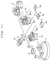
- the transfer robots 24a and 24b may be a mobile type robot which moves along rails shown in FIG. 10, or a stationary type robot having robot hands at forward ends of articulated arms shown in FIG. 11.
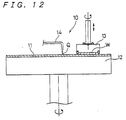
- the polishing section 10 comprises a turntable 12 having a polishing cloth 11 thereon, a top ring 13 for supporting a semiconductor wafer (substrate) W and pressing the semiconductor substrate W against the turntable 12, and a nozzle 14 for supplying an abrasive liquid onto the polishing cloth 11.
- a transfer device 38 is disposed adjacent to the turntable 12. The adjacent two sections are partitioned by a partition wall to prevent cross-contamination. Specifically, in order to prevent dirty atmosphere in the polishing section 10 from being scattered into a chamber in which a cleaning process and a subsequent process are performed, air conditioning and pressure regulation in each of the chambers are performed.
- the semiconductor substrate W is transported from the load and unload section 22 to the transfer device 38 by the transfer robots 24a and 24b and transferred to the top ring 13 by the transfer device 38.
- the semiconductor substrate W is held by the lower surface of the top ring 13 and pressed against the polishing cloth 11 providing a polishing surface on the turntable 12.
- the abrasive liquid Q is supplied from the nozzle 14 onto the polishing cloth 11 and retained on the polishing cloth 11.
- the top ring 13 exerts a certain pressure on the turntable 12, and the surface of the semiconductor substrate W held against the polishing cloth 11 is therefore polished in the presence of the abrasive liquid Q between the surface of the semiconductor substrate W and the polishing surface on the polishing cloth 11 by a combination of chemical polishing and mechanical polishing while the top ring 13 and the turntable 12 are rotated.
- the abrasive liquid Q contains abrasive particles having a certain diameter suspended in an alkali solution.
- the primary cleaning unit 26a in the cleaning section 26 has a plurality of vertical spindles 30 arranged at spaced intervals for supporting the outer circumferential edge of the semiconductor substrate W by their holding grooves formed at the upper end portions of the spindles 30 and rotating the semiconductor substrate in a horizontal plane at a relatively low rotational speed, and a pair of cleaning members comprising a roller type or a pencil type sponge which can be brought in contact with the semiconductor substrate W or out of contact with the semiconductor substrate W.
- the primary cleaning unit 26a is a low rotational speed type cleaning unit.
- the secondary and tertiary cleaning units 26b and 26c have a rotating table 36 comprising a rotating shaft 32 and a plurality of arms 34 which extend radially outwardly from the rotating shaft 32 and hold the outer circumferential edge of the semiconductor substrate W.
- the secondary and tertiary cleaning units 26b and 26c are a high rotational speed type cleaning unit.
- a nozzle for supplying a cleaning liquid to the surface of the semiconductor substrate W
- a cover for preventing the cleaning liquid from being scattered around
- a ventilating equipment for creating down draft (descending air current) to prevent mist from being scattered around.
- the cleaning processes for cleaning the semiconductor substrate which has been polished are carried out in the following manner:
- a scrubbing cleaning is performed by allowing the cleaning members to scrub the upper and lower surfaces of the semiconductor substrate W while supplying a cleaning liquid.
- the first cleaning liquid having substantially the same pH as the abrasive liquid used in the polishing process is used to prevent particles from being aggregated due to so-called pH shock.
- the pH shock is defined as a rapid change of a pH.
- the first cleaning liquid having substantially the same pH as the abrasive liquid is used in the scrubbing cleaning process.
- aqueous ammonia is used as the first cleaning liquid, and after the particles are removed from the surfaces of the semiconductor substrate W, the surfaces of the semiconductor substrate are shifted from alkali to neutrality by supplying a neutral cleaning liquid such as pure water thereto. Thereafter, the semiconductor substrate W is transferred to the secondary cleaning unit 26b.
- the secondary cleaning unit 26b in order to remove metal ion attached to the semiconductor substrate W, acid chemicals is normally supplied to the surfaces of the semiconductor substrate W from the nozzle to cause etching (chemical cleaning) of the surfaces of the semiconductor substrate, and then a neutral cleaning liquid such as pure water is supplied to cause the surfaces of the semiconductor substrate to be returned to neutrality. Thereafter, the semiconductor substrate W is transferred to the tertiary cleaning unit 26c having a drying function. In the tertiary cleaning unit 26c, pure water is supplied to perform a final cleaning of the semiconductor substrate W, and then the semiconductor substrate W is rotated at a high rotational speed while blowing a clean inert gas against the surfaces of the semiconductor substrate, thereby drying the semiconductor substrate W. After the semiconductor substrate W is cleaned and dried, the semiconductor substrate W is returned to the load and unload section 22 by clean hand of the transfer robot 24a or 24b.
- a neutral cleaning liquid such as pure water
- the polishing apparatus since the etching cleaning is conducted by the dedicated cleaning unit, i.e., the cleaning processes are conducted by the three cleaning units 26a, 26b and 26c, the polishing apparatus becomes large, requires a large installation space, and needs a long processing time for the cleaning processes.
- the semiconductor substrate W is transported as shown by arrows 1 ⁇ to 9 ⁇ in FIG. 11, and hence the transportation route is extremely complicated. Specifically, the semiconductor substrate is transported from the load and unload section 22 to the reversing device 28 as shown by the arrow 1 ⁇ , transported to the transfer device 38 as shown by the arrow 2 ⁇ , and then moved above the turntable 12 as shown by the arrow 3 ⁇ . Thereafter, the polished semiconductor substrate W is moved to the transfer device 38 as shown by the arrow 4 ⁇ , transported to the primary cleaning unit 26a as shown by the arrow 5 ⁇ , and then transported to the reversing device 28 as shown by the arrow 6 ⁇ .
- the semiconductor substrate W is transported to the secondary cleaning unit 26b as shown by the arrow 7 ⁇ , and then transferred to the tertiary cleaning unit 26c as shown by the arrow 8 ⁇ . Finally, the semiconductor substrate W is returned to the load and unload section 22 as shown by the arrow 9 ⁇ .
- the cleaning section 26 it is conceivable to conduct the primary cleaning process for removing particles and the secondary cleaning process for etching by the same cleaning unit.
- alkali chemicals and acid chemicals are employed as the respective cleaning liquids in the same cleaning unit, and hence the lining of the drainage is deteriorated, salt is deposited, and waste water treatment is complicated.
- the semiconductor substrate W is dried in the atmosphere in which mist of the etching liquid remains, and hence the semiconductor substrate is contaminated in the final cleaning process.
- the polishing apparatus includes a storage cassette for storing workpieces to be polished, at least two polishing units each having at least a turntable with a polishing cloth mounted thereon and a top ring for supporting a workpiece and pressing the workpiece against the polishing cloth, and a cleaning unit for cleaning a workpiece which has been polished by either one of the polishing units in such a state that the workpiece is removed from the top ring.
- the polishing apparatus further includes a transfer robot for transferring a workpiece between two of the storage cassette, the polishing units and the cleaning unit.
- a cleaning apparatus for cleaning a substrate which has been polished as set forth in claim 1 is provided.
- Preferred embodiments are disclosed in the dependent claims.
- the present invention is directed to provide a method and apparatus for polishing substrates with an optimum structure.
- a polishing apparatus for polishing and then cleaning a substrate, the apparatus comprising: a polishing section having at least one polishing unit for performing a primary polishing and a secondary polishing of the substrate by pressing the substrate against a polishing surface; a cleaning section for cleaning the substrate which has been polished to remove particles attached to the substrate by a scrubbing cleaning, and removing metal ion from the substrate by supplying an etching liquid.
- the substrate is polished at a polishing efficiency lower than the primary polishing in such a manner that the polishing pressure and/or the polishing rate are smaller than those of the primary polishing.
- polishing efficiency lower than the primary polishing in such a manner that the polishing pressure and/or the polishing rate are smaller than those of the primary polishing.
- the substrate having a trace of particles thereon is transported to the cleaning section, and hence a process for removing particles by alkali can be eliminated, differently to the conventional method.
- etching of the surface of the substrate which is a kind of chemical cleaning using acid can be conducted, and then the substrate is cleaned and dried by a cleaning and drying process.
- cleaning and drying of the substrate can be performed by two cleaning units and two processes, and thus the processing time is shortened and the number of apparatuses or units can be reduced, compared with the conventional apparatus and method. Further, the number of times in transporting the substrate is reduced, and hence load in processes can be reduced and the chance of contamination of the substrate can be reduced.
- the cleaning liquid or the etching liquid may be supplied to the front and backside surfaces of the substrate.
- the drying process may be performed by the drying unit different from the cleaning unit or the same cleaning unit. If the drying process is performed by the same cleaning unit, then it is desirable to perform the drying process in the clean atmosphere.
- a cleaning liquid a high performance water including ionic water, ozone water, and hydrogen water may be used.
- the primary polishing and the secondary polishing are conducted in the same polishing unit. This constitution allows the polishing apparatus to be simplified and to reduce an installation space thereof.
- the polishing section comprises at least two polishing units for performing the primary polishing and the secondary polishing, respectively. This constitution allows the processes to be simplified and contributes to improving throughput of the substrates.
- the polishing section comprises at least two polishing units for the primary polishing process and the secondary polishing process
- the cleaning section comprises at least two cleaning units for performing different cleaning processes. This constitution allows two-stage cleaning or three-stage cleaning, and a plurality of cleaning processes can be performed by the single apparatus.
- the two-stage cleaning and the three-stage cleaning can be selectively performed. If the abrasive liquid and the polishing cloth are replaced in the polishing unit, then an optimum apparatus which is suitable for both of the process which uses the abrasive liquid containing siliceous material and the process which uses the abrasive liquid containing alumina material may be constructed. Further, even if the scrubbing process becomes unnecessary due to progress in the polishing technology with use of the abrasive liquid containing alumina material and the cleaning technology after polishing, the present invention offers an optimum structure.
- a polishing method for polishing and then cleaning a substrate comprising: polishing the substrate primarily by pressing the substrate against a polishing surface; polishing the substrate secondarily at a polishing rate lower than the primary polishing; cleaning the substrate which has been polished to remove particles attached to the substrate by a scrubbing cleaning, and removing metal ion from the substrate by supplying an etching liquid; and drying the substrate after removing the metal ion therefrom.
- the etching liquid comprises acid aqueous solution containing hydrofluoric acid.
- a cleaning apparatus for cleaning a substrate which has been polished comprising: at least two primary cleaning units having the same cleaning function, each for primarily cleaning the substrate which has been polished; and a common secondary cleaning unit for secondarily cleaning the substrate which has been cleaned by the primary cleaning units.
- the primary cleaning of the substrates is conducted in parallel in the primary cleaning units simultaneously or with a certain time lag, and then the secondary cleaning of the substrates which have been primarily cleaned is conducted in a common secondary cleaning unit.
- This arrangement is desirable for such a case where the primary cleaning need time longer than the secondary cleaning.
- a cleaning apparatus for cleaning a substrate which has been polished comprising: at least three cleaning units for cleaning the substrate which has been polished; and a transfer robot for transferring the substrate between at least two of the cleaning units; wherein the substrate is cleaned by selective cleaning processes conducted by any two or three cleaning units selected from the at least three cleaning units.
- any two or three cleaning units are selected from at least three cleaning units to conduct selective cleaning processes of the substrates.
- the selective cleaning processes include two-stage cleaning of the substrate or three-stage cleaning of the substrate.
- a polishing apparatus for polishing and then cleaning a substrate, the apparatus comprising: a plurality of polishing units for polishing the substrate; and a plurality of cleaning units for cleaning the substrate which has been polished; wherein the substrates are processed by different processes through a plurality of polishing-cleaning routes, each including at least one selected from the polishing units and at least one selected from the cleaning units.
- At least one selected from a plurality of polishing units and at least one selected from a plurality of cleaning units can be combined to construct a polishing-cleaning route, and the number of polishing-cleaning routes can be freely selected by setting the number of polishing units and cleaning units appropriately, and hence a plurality of different processes can be selectively conducted on the substrates.
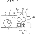
- FIGS. 1 through 5 show a polishing apparatus according to a first design.
- the polishing apparatus comprises a polishing section 10 having one polishing unit, and a cleaning section 26 having two transfer robots 24a and 24b and two cleaning units 26a and 26b.
- the polishing section 10 and the transfer robots 26a and 26b have the same structure as the conventional ones.
- the polishing cloth 11 on the turntable 12 constitutes a polishing surface.
- the polishing section 10 and the cleaning units 26a and 26b are partitioned by respective partition walls, and are evacuated independently to prevent respective atmospheres from being mixed.
- the primary cleaning unit 26a in the cleaning section 26 includes six vertical spindles 30 that are arranged at spaced intervals along a circle for supporting the outer circumferential edge of a semiconductor substrate W and rotating the semiconductor substrate W in a horizontal plane at a relatively low rotational speed, and a pair of roller type cleaning members 40 made of sponge, PVA or the like and extending horizontally diametrically above and below the semiconductor substrate W.
- the vertical spindles 30 are movable horizontally toward and away from the semiconductor substrate W.
- the cleaning members 40 can be brought in contact with the semiconductor substrate W or out of contact with the semiconductor substrate W.
- the primary cleaning unit 26a is a roll and low rotational speed type cleaning unit.
- nozzles 50a, 50b, 50c and 50d for supplying an etching liquid and pure water to the upper and lower surfaces of the semiconductor substrate W.
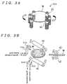
- the secondary cleaning unit 26b comprises a rotating table 36 for rotating the semiconductor substrate W at a high rotational speed of 1500 to 5000 rpm, and a swing arm 44 having a nozzle 42 for supplying a cleaning liquid to which ultrasonic vibration is applied to the upper surface of the semiconductor substrate W.
- the secondary cleaning unit 26b is a megasonic and high rotational speed type cleaning unit.
- the secondary cleaning unit 26b may include a nozzle 46 for supplying an inert gas to the surface of the semiconductor substrate W or a heater for speeding up drying of the semiconductor substrate W to improve process performance and shorten tact time. Further, the secondary cleaning unit 26b may include a nozzle for supplying a cleaning liquid to the lower surface of the semiconductor substrate W.
- noncontact type cleaning is performed by supplying the cleaning liquid to which ultrasonic vibration is applied by an ultrasonic vibration generating device (not shown) from the nozzle 42 to the semiconductor substrate W
- a pencil type cleaning member made of sponge or the like may be replaced with the nozzle 42 or may be added other than the nozzle 42 to perform contact type cleaning.
- the semiconductor substrate W is transported from the load and unload section 22 to the polishing section 10 via the reversing device 28 and the transfer device 38 by the transfer robots 24a and 24b as shown by the arrows 1 ⁇ , 2 ⁇ and 3 ⁇ .
- the semiconductor substrate W is held by the lower surface of the top ring 13 and pressed against the polishing cloth 11 on the turntable 12.
- the normal abrasive liquid is used to polish the semiconductor substrate W.
- This polishing process is referred to as "normal polishing" or "main polishing”.
- a water polishing process is conducted in the polishing section 10.
- the polishing rate in the water polishing process is preferably 100 ⁇ (angstrom)/minute or below, and microscratches on the polished surface of the semiconductor substrate W formed in the normal polishing are removed or reduced, and the ground-off particles and the abrasive particles remaining on the polished surface are removed.
- finish polishing process is so-called "finish polishing process”.
- This finish polishing process may be performed using a polishing liquid containing abrasive particles smaller than the abrasive particles used in the normal polishing process, or chemicals instead of the water polishing process, or between the normal polishing process and the water polishing process.
- the finish polishing process is performed on the same turntable as the normal polishing process in this design, the finish polishing may be conducted by a discrete turntable.
- the abrasive liquid containing the abrasive particles remains on the polishing cloth 11 immediately after the normal polishing process, it is necessary to supply a certain amount of pure water to the polishing cloth 11 to remove the abrasive liquid therefrom.
- a large amount of pure water is rapidly supplied to the polishing cloth 11 to dilute the abrasive liquid, then the pH of the abrasive liquid remaining on the polished surface of the semiconductor substrate and the polishing cloth 11 is rapidly changed to cause the abrasive particles to be aggregated due to the pH shock. Therefore, it is desirable that a small amount of pure water is first supplied, and the supply of pure water is gradually increased.
- the particles aggregated on the polished surface of the semiconductor substrate will be removed in the finish polishing process described below, and thus a serious problem does not arise.
- the particles attached to the semiconductor substrate W are mostly removed to allow the semiconductor substrate W to enhance a degree of cleanliness.
- the semiconductor substrate W is transported to the primary cleaning unit 26a via the transfer device 38 as shown by the arrows 4 ⁇ and 5 ⁇ by the transfer robot 24a.
- the semiconductor substrate W is held by the spindles 30.
- the semiconductor substrate W may be rotated at a low rotational speed of several 10 rpm to 300 rpm by the spindles 30.
- the scrubbing cleaning of the upper and lower surfaces of the semiconductor substrate W is performed by rotating the cleaning members 40 about their own axes while supplying pure water from the nozzles to the surfaces of the semiconductor substrate W.
- the etching liquid is supplied to the upper and lower surfaces of the semiconductor substrate W from the nozzles while the rotational speed of the semiconductor substrate W is being changed as necessary.
- metal ion remaining on the semiconductor substrate W is removed by etching (chemical cleaning) of the surfaces of the semiconductor substrate W.
- pure water is supplied from the pure water nozzles, and the etching liquid is removed by replacing the etching liquid with pure water while the rotational speed of the semiconductor substrate W is being changed as necessary.
- the semiconductor substrate W is transported to the reversing device 28, reversed to direct the polished surface upwardly, and then transported to the secondary cleaning unit 26b by the transfer robots 24a and 24b as shown by the arrows 6 ⁇ and 7 ⁇ in FIG. 2.
- the secondary cleaning unit 26b as shown in FIGS.
- the swing arm 44 is swung over the entire surface of the semiconductor substrate W while pure water to which ultrasonic vibration is applied is supplied from the nozzle 42 provided at the forward end of the swing arm 44 to the upper surface of the semiconductor substrate W so as to allow the supplied pure water to pass through the center of the semiconductor substrate W, thereby removing particles from the semiconductor substrate W. Thereafter, the supply of pure water is stopped, the swing arm 44 is moved to the standby position, and then the semiconductor substrate W is rotated at a high rotational speed of 150 to 5000 rpm to dry the semiconductor substrate W while supplying an inert gas as necessary.
- the semiconductor substrate W which has been dried is returned to a wafer cassette 22a or 22b placed on the load and unload section 22 by the transfer robot 24b as shown by the arrow 8 ⁇ in FIG. 2.
- the number of the cleaning units in the cleaning section 26 is reduced from three units to two units, and the number of times in transporting the semiconductor substrate w is also reduced from nine as shown in FIG. 11 to eight as shown in FIG. 2.
- the total processing time is greatly shortened.
- the transportation route of the semiconductor substrate W is simplified, the chance of interference of the transfer robots 24a and 24b with each other is decreased, and control of the transfer robots 24a and 24b is facilitated.
- the structure of the cleaning units 26a and 26b is not limited to the above-mentioned structure, and, for example, the cleaning member 40 may comprise a brush or a felt-like fiber, or the cleaning liquid may be a cleaning liquid to which cavitation is applied, or minute particles of ice.
- the number of the cleaning units 26a and 26b is set to an optimum number in consideration of tact time in the respective cleaning units.
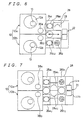
- FIG. 6 shows a polishing apparatus according to a first embodiment of the present invention.
- two polishing units 10a and 10b having the same structure as the polishing unit in FIG. 1 are provided in the polishing section 10, and one transfer robot 24a which moves along rails is provided.
- the two polishing units 10a and 10b are disposed symmetrically with respect to the moving path of the transfer robot 24a.
- primary cleaning units 26a 1 and 26a 2 which have the same cleaning function and the same structure with each other are provided so as to correspond to the respective polishing units 10a and 10b, and one secondary cleaning unit 26b is provided.
- Other structure of the polishing apparatus shown in FIG. 6 is substantially the same as that of the polishing apparatus shown in FIG. 1.
- a parallel processing in which the semiconductor substrates W are polished by the polishing units 10a and 10b in parallel and a serial processing in which one semiconductor substrate W is polished sequentially by the polishing units 10a and 10b can be performed.
- the normal polishing and the water polishing are conducted in the polishing units 10a and 10b, respectively, with a certain time lag, to thereby perform efficient transfer of the semiconductor substrates W by the transfer robot 24a.
- the operating efficiency in the transfer robots and the cleaning section is not high in the polishing apparatus of FIG. 1, but the operating efficiency in the transfer robot 24a and the cleaning section 26 is high in the polishing apparatus of FIG. 6 because there are provided the two polishing units 10a and 10b.
- the throughput per unit area of floor occupied by the overall polishing apparatus can be improved.
- the primary cleaning units 26a 1 and 26a 2 are provided so as to correspond to the respective polishing units 10a and 10b, operational delay in the cleaning section 26 can be prevented.
- the normal polishing of the semiconductor substrate W is performed in the polishing unit 10a, and then the polished semiconductor substrate W is transferred to the polishing unit 10b in which the water polishing is performed. If the problem of contamination of the semiconductor substrate does not arise, then the normal polishing of the semiconductor substrate W is conducted in the polishing unit 10a, and then the polished semiconductor substrate W is transferred to the polishing unit 10b by the transfer robot 24a. If the problem of contamination of the semiconductor substrate arises, then the normal polishing of the semiconductor substrate W is conducted in the polishing unit 10a, the polished semiconductor substrate W is transferred to the primary cleaning unit 26a 1 , by the transfer robot 24a, in which it is cleaned.
- the cleaned semiconductor substrate W is transferred to the polishing unit 10b in which the finish polishing of the semiconductor substrate W is conducted. Further, in the primary cleaning unit 26a 1 , the semiconductor substrate W may be cleaned using chemicals suitable for the slurry (abrasive liquid) used in the polishing unit 10a.
- two primary cleaning units 26a 1 and 26a 2 and one secondary cleaning unit 26b are provided. This is because primary cleaning process takes more time than secondary cleaning process.
- two primary cleaning units 26a 1 and 26a 2 are provided to improve efficiency each for the polishing unit 10a and the polishing unit 10b, while the secondary cleaning unit 26b which needs the processing time shorter than the primary cleaning process is used in common for the substrates which are cleaned in both the primary cleaning units 26a 1 and 26a 2 .
- FIG. 7 shows a polishing apparatus according to a second design.
- the polishing section 10 has two polishing units 10a and 10b having the same structure as the polishing unit of FIG. 1.
- the polishing units 10a and 10b are symmetrically disposed in the same manner as the polishing apparatus of FIG. 6.
- primary cleaning units 26a 1 and 26a 2 having the same structure
- secondary cleaning units 26b 1 and 26b 2 having the same structure
- reversing devices 28a 1 and 28a 2 are symmetrically disposed so as to correspond to the polishing units 10a and 10b, respectively.
- a parallel processing and a serial processing can be conducted.
- the parallel processing In the parallel processing, the first substrate processing line A in which the polishing process conducted by the polishing unit 10a, the primary cleaning process conducted by the primary cleaning unit 26a 1 , and the secondary cleaning process conducted by the secondary cleaning unit 26b 1 are sequentially performed, and the second substrate processing line B in which the polishing process conducted by the polishing unit 10b, the primary cleaning process conducted by the primary cleaning unit 26a 2 and the secondary cleaning process conducted by the secondary cleaning unit 26b 2 are sequentially performed can be constructed. Therefore, the parallel processing can be independently conducted without causing the two transfer lines of the semiconductor substrates W to intersect.
- two parallel processing can be conducted.
- the semiconductor substrates W taken out from one wafer cassette are alternately delivered to the respective polishing units 10a and 10b.
- This parallel processing allows the processing time of one wafer cassette to be halved.
- the wafer cassette 22a is assigned exclusively to the first substrate processing line A
- another wafer cassette 22b is assigned exclusively to the second substrate processing line B.
- the semiconductor substrates W to be polished may be the same ones or different ones.
- four wafer cassettes may be placed on the load and unload section 22 to thereby conduct continuous processing of the semiconductor substrates.
- the first substrate processing line A and the second substrate processing line B may have their own processing units or devices, and hence two kinds of different processes can be performed in parallel in the polishing apparatus. Further, it is conceivable to incorporate a cleaning device using ultrasonic vibration in the second cleaning unit 26 b 1 and to incorporate a cleaning device using cavitation in the secondary cleaning unit 26b 2 . This structure allows the polishing apparatus to have versatile functions performed by two polishing apparatuses shown in FIG. 1.
- each of the cleaning units including the primary cleaning units 26a 1 and 26a 2 , the secondary cleaning units 26b 1 and 26b 2 may be modulized, and may be separable from the polishing apparatus and replaceable. According to this structure, even after the polishing apparatus is installed, the polishing apparatus can comply with various required processes. Further, in the event of failure in the cleaning unit, or in case of maintenance of the cleaning unit, the down time of the polishing apparatus can be shortened to raise the operation rate thereof.
- FIG. 8 shows a polishing apparatus according to a second embodiment of the present invention.
- the polishing section 10 comprises two polishing units 10a and 10b having the same structure as the polishing unit of FIG. 1, and the polishing units 10a and 10b are disposed symmetrically.
- the cleaning section 26 there are provided primary cleaning units 26a 1 and 26a 2 which have same cleaning function and same structure with each other, a secondary cleaning unit 26b and a tertiary cleaning unit 26c.
- reversing devices 28a 1 and 28a 2 are symmetrically provided so as to correspond to the polishing units 10a and 10b, respectively.
- the secondary cleaning unit 26b comprises a nozzle 42 for supplying a cleaning liquid to which ultrasonic vibration is applied to the semiconductor substrate W, and a cleaning member such as a pencil type sponge for scrubbing the semiconductor substrate W by bringing the cleaning member in contact with the semiconductor substrate W. That is, the secondary cleaning unit 26b is a pencil and megasonic and mechanical chuck type cleaning unit having a drying function.
- the tertiary cleaning unit 26c having a drying function comprises a cleaning member such as a pencil type sponge, and is a pencil and mechanical chuck type cleaning unit.
- the three-stage cleaning in addition to the two-stage cleaning, the three-stage cleaning can be performed, and hence a plurality of cleaning methods can be conducted in the single polishing apparatus.
- the two-stage cleaning in which the primary cleaning process conducted by the primary cleaning unit 26a 1 , the secondary cleaning process conducted by the tertiary cleaning unit 26c, and the spin-drying process are performed sequentially, and the three-stage cleaning in which the primary cleaning process conducted by the primary cleaning unit 26a 1 , the secondary cleaning process conducted by the secondary cleaning unit 26b, the tertiary cleaning process conducted by the tertiary cleaning unit 26c, and the spin-drying process are performed sequentially can be conducted.
- the two-stage cleaning in which the primary cleaning process conducted by the primary cleaning unit 26a 2 , the secondary cleaning process conducted by the secondary cleaning unit 26b or the tertiary cleaning unit 26c, and the spin-drying process are performed sequentially, and the three-stage cleaning in which the primary cleaning process conducted by the primary cleaning unit 26a 2 , the secondary cleaning process conducted by the secondary cleaning unit 26b, the tertiary cleaning process conducted by the tertiary cleaning unit 26c, and the spin-drying process are performed sequentially can be conducted.
- polishing processes 1 ⁇ to 5 ⁇ can be conducted. That is, one semiconductor substrate is processed in the following route.
- the cleaning process can be selected to achieve optimum characteristic of the polished surface of the semiconductor substrate and also high throughput.
- four cleaning units which perform different three kinds of cleaning processes are used to perform two-stage cleaning or three-stage cleaning.
- four cleaning units which perform four kinds of different cleaning processes, or more cleaning units may be used to perform four-stage cleaning.
- a plurality of cleaning units which perform different cleaning processes may be modularized, and may be separable from the polishing apparatus and replaceable to thereby comply with various processes.
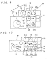
- FIG. 9 shows a polishing apparatus according to a third design.
- a small-sized finish polishing unit 10c which performs water polishing is provided in the polishing section 10.
- the finish polishing unit 10c has a finish polishing table 12c having a diameter slightly larger than the semiconductor substrate W to be polished.
- the finish polishing table 12c does not rotate about its own axis, but performs a circulatory translational motion in a horizontal plane. This circulatory translational motion is referred to as "orbital motion" or "scroll motion".
- This circulatory translational motion is achieved by the structure in which a driving end provided eccentrically at an upper end of a driving shaft of a motor is accommodated in a recess formed in a lower surface of the finish polishing table through a bearing, and the rotation of the finish polishing table about its own axis is mechanically restrained. Further, since the water polishing time is shorter than the normal polishing time, in addition to the polishing unit shown in FIG. 9, a polishing unit which performs a second normal polishing may be provided to thereby achieve further high throughput.
- a material softer than the normal polishing cloth is preferably used.
- the polishing cloth which is commercially available are nonwoven fabric cloth made of polyester, and Politex, Suba 800 and IC-1000 manufactured by Rodel Products Corporation, and Surfin xxx-5 and Surfin 000 manufactured by Fujimi Inc.
- the polishing cloth sold under the tradenames Suba 800, Surfin xxx-5, and Surfin 000 is made of nonwoven fabric composed of fibers bound together by urethane resin, and the polishing cloth sold under the tradename IC-1000 is made of polyurethane.
- the wiping cloth which is commercially available are Miracle Series (tradename) sold by Toray Industries, Inc., and Minimax (tradename) sold by Kanebo, Ltd. These wiping cloth have a number of fibers, having a diameter of 1 to 2 ⁇ m, of 15500-31000/cm 2 (a hundred thousand to two hundred thousand per in 2 ) in high density manner, and have a large number of contacting points contacting the object to be wiped, and thus have an excellent ability for wiping fine particles. Since the wiping cloth is a thin cloth, it is desirable that the wiping cloth is attached to the polishing table through a cushioning member such as a sponge or a rubber so as not to damage the semiconductor substrate during finish polishing.
- a cushioning member such as a sponge or a rubber
- the polishing pressure is 0-200 g/cm 2
- the relative speed between the polishing table and the semiconductor substrate is 0.07-0.6 m/sec
- the processing time is 10 - 120 second.
- the polishing apparatus offers throughput higher than that of the polishing apparatus of FIG. 1, and occupies an installation floor area smaller than that of the polishing apparatus of FIG. 6. Further, since the finish polishing unit 10c for exclusively performing water polishing is provided, the polishing apparatus has an excellent finish processing capability in which there exists few scratches and few particles on the polished surface of the semiconductor substrate.
- the cloth for finish polishing (water polishing) attached to the finish polishing table 12c may be applied to the polishing unit 10b which is used for water polishing in the serial processing in FIG. 6.
- polishing SiO 2 layer on the semiconductor substrate W has been described in the above embodiments, the present invention is not limited to those embodiments.
- polishing metal layer such as CU layer
- diluted hydrofluoric acid or acid aqueous solution containing HCl may be used as an etching liquid in the primary cleaning unit.
- the processing time can be shortened and the cost of the polishing apparatus can be reduced, compared with the conventional apparatus. Further, since the number of times in transporting the semiconductor substrate is reduced, the processes are simplified and the chance of the contamination of the semiconductor substrate is reduced. Therefore, the processing time is shortened and the semiconductor substrate having a high degree of cleanliness may be obtained by the small-sized apparatus.
Description
Claims (3)
- A cleaning apparatus (26) for cleaning a substrate which has been polished, said apparatus comprising:at least two primary cleaning units (26a1, 26a2) having the same cleaning function, each for primarily cleaning the substrate which has been polished; anda common secondary cleaning unit (26b) for secondarily cleaning the substrate which has been cleaned by said primary cleaning units (26a1, 26a2).
- A cleaning apparatus (26) according to clam 1, further comprising a drying unit for drying the substrate after said secondarily cleaning.
- A cleaning apparatus (26) according to claim 1, wherein one of said cleaning comprises cleaning the substrate by supplying an etching liquid.
Priority Applications (1)
| Application Number | Priority Date | Filing Date | Title |
|---|---|---|---|
| EP05015086A EP1600258A1 (en) | 1998-11-06 | 1999-11-08 | Method and apparatus for polishing substrate |
Applications Claiming Priority (6)
| Application Number | Priority Date | Filing Date | Title |
|---|---|---|---|
| JP31652298 | 1998-11-06 | ||
| JP31652298 | 1998-11-06 | ||
| JP13870599 | 1999-05-19 | ||
| JP13870599 | 1999-05-19 | ||
| JP23677699 | 1999-08-24 | ||
| JP23677699A JP3979750B2 (en) | 1998-11-06 | 1999-08-24 | Substrate polishing equipment |
Related Child Applications (1)
| Application Number | Title | Priority Date | Filing Date |
|---|---|---|---|
| EP05015086.1 Division-Into | 2005-07-12 |
Publications (3)
| Publication Number | Publication Date |
|---|---|
| EP0999012A2 EP0999012A2 (en) | 2000-05-10 |
| EP0999012A3 EP0999012A3 (en) | 2003-01-29 |
| EP0999012B1 true EP0999012B1 (en) | 2005-09-07 |
Family
ID=27317724
Family Applications (2)
| Application Number | Title | Priority Date | Filing Date |
|---|---|---|---|
| EP99122248A Expired - Lifetime EP0999012B1 (en) | 1998-11-06 | 1999-11-08 | Method and apparatus for polishing substrate |
| EP05015086A Withdrawn EP1600258A1 (en) | 1998-11-06 | 1999-11-08 | Method and apparatus for polishing substrate |
Family Applications After (1)
| Application Number | Title | Priority Date | Filing Date |
|---|---|---|---|
| EP05015086A Withdrawn EP1600258A1 (en) | 1998-11-06 | 1999-11-08 | Method and apparatus for polishing substrate |
Country Status (6)
| Country | Link |
|---|---|
| US (3) | US6494985B1 (en) |
| EP (2) | EP0999012B1 (en) |
| JP (1) | JP3979750B2 (en) |
| KR (1) | KR100632412B1 (en) |
| DE (1) | DE69927111T2 (en) |
| TW (1) | TW445537B (en) |
Cited By (1)
| Publication number | Priority date | Publication date | Assignee | Title |
|---|---|---|---|---|
| EP1600258A1 (en) * | 1998-11-06 | 2005-11-30 | Ebara Corporation | Method and apparatus for polishing substrate |
Families Citing this family (41)
| Publication number | Priority date | Publication date | Assignee | Title |
|---|---|---|---|---|
| US6526995B1 (en) * | 1999-06-29 | 2003-03-04 | Intersil Americas Inc. | Brushless multipass silicon wafer cleaning process for post chemical mechanical polishing using immersion |
| EP1077474A3 (en) | 1999-08-14 | 2004-05-12 | Applied Materials, Inc. | Backside etching in a scrubber |
| JP2001326201A (en) * | 2000-05-16 | 2001-11-22 | Ebara Corp | Polishing device |
| US20020023715A1 (en) * | 2000-05-26 | 2002-02-28 | Norio Kimura | Substrate polishing apparatus and substrate polishing mehod |
| US6953392B2 (en) * | 2001-01-05 | 2005-10-11 | Asm Nutool, Inc. | Integrated system for processing semiconductor wafers |
| US7172497B2 (en) | 2001-01-05 | 2007-02-06 | Asm Nutool, Inc. | Fabrication of semiconductor interconnect structures |
| TWI222154B (en) * | 2001-02-27 | 2004-10-11 | Asm Nutool Inc | Integrated system for processing semiconductor wafers |
| US20040259348A1 (en) * | 2001-02-27 | 2004-12-23 | Basol Bulent M. | Method of reducing post-CMP defectivity |
| US7204743B2 (en) * | 2001-02-27 | 2007-04-17 | Novellus Systems, Inc. | Integrated circuit interconnect fabrication systems |
| JP2003021818A (en) * | 2001-07-05 | 2003-01-24 | Toshiba Corp | Method for manufacturing flat panel display element |
| US20030022498A1 (en) * | 2001-07-27 | 2003-01-30 | Jeong In Kwon | CMP system and method for efficiently processing semiconductor wafers |
| CN1329972C (en) * | 2001-08-13 | 2007-08-01 | 株式会社荏原制作所 | Semiconductor device, method for manufacturing the same, and plating solution |
| US6638145B2 (en) * | 2001-08-31 | 2003-10-28 | Koninklijke Philips Electronics N.V. | Constant pH polish and scrub |
| JP2003077871A (en) * | 2001-09-04 | 2003-03-14 | Komatsu Machinery Corp | Planar grinding system of semiconductor wafer and working method therefor |
| JP4101609B2 (en) * | 2001-12-07 | 2008-06-18 | 大日本スクリーン製造株式会社 | Substrate processing method |
| US6863595B1 (en) * | 2001-12-19 | 2005-03-08 | Cypress Semiconductor Corp. | Methods for polishing a semiconductor topography |
| US7077916B2 (en) * | 2002-03-11 | 2006-07-18 | Matsushita Electric Industrial Co., Ltd. | Substrate cleaning method and cleaning apparatus |
| JP2003318151A (en) * | 2002-04-19 | 2003-11-07 | Nec Electronics Corp | Method of manufacturing semiconductor device |
| DE10229000A1 (en) * | 2002-06-28 | 2004-01-29 | Advanced Micro Devices, Inc., Sunnyvale | Device and method for reducing the oxidation of polished metal surfaces in a chemical mechanical polishing process |
| KR100487562B1 (en) * | 2003-03-24 | 2005-05-03 | 삼성전자주식회사 | Method of fabricating semiconductor for reducing wafer warpage |
| JP4698144B2 (en) | 2003-07-31 | 2011-06-08 | 富士通セミコンダクター株式会社 | Manufacturing method of semiconductor device |
| US20050106359A1 (en) * | 2003-11-13 | 2005-05-19 | Honeywell International Inc. | Method of processing substrate |
| US20060077817A1 (en) * | 2004-09-13 | 2006-04-13 | Seo Kang S | Method and apparatus for reproducing data from recording medium using local storage |
| US7993485B2 (en) * | 2005-12-09 | 2011-08-09 | Applied Materials, Inc. | Methods and apparatus for processing a substrate |
| US20070131653A1 (en) * | 2005-12-09 | 2007-06-14 | Ettinger Gary C | Methods and apparatus for processing a substrate |
| KR100744222B1 (en) * | 2005-12-27 | 2007-07-30 | 동부일렉트로닉스 주식회사 | Chemical-mechanical polishing system |
| JP5204960B2 (en) | 2006-08-24 | 2013-06-05 | 株式会社フジミインコーポレーテッド | Polishing composition and polishing method |
| US8205625B2 (en) * | 2006-11-28 | 2012-06-26 | Ebara Corporation | Apparatus and method for surface treatment of substrate, and substrate processing apparatus and method |
| JP5258082B2 (en) * | 2007-07-12 | 2013-08-07 | 東京エレクトロン株式会社 | Substrate processing apparatus and substrate processing method |
| US7670438B2 (en) * | 2007-10-03 | 2010-03-02 | United Microelectronics Corp. | Method of removing particles from wafer |
| CN101419903B (en) * | 2007-10-24 | 2010-06-23 | 联华电子股份有限公司 | Method for removing granules on wafer |
| JP5306644B2 (en) * | 2007-12-29 | 2013-10-02 | Hoya株式会社 | Manufacturing method of mask blank substrate, manufacturing method of substrate with multilayer reflective film, manufacturing method of reflecting mask blank, and manufacturing method of reflecting mask |
| US8795032B2 (en) * | 2008-06-04 | 2014-08-05 | Ebara Corporation | Substrate processing apparatus, substrate processing method, substrate holding mechanism, and substrate holding method |
| WO2010044325A1 (en) * | 2008-10-17 | 2010-04-22 | コニカミノルタオプト株式会社 | Process for producing glass substrate, and process for producing magnetic recording medium |
| US8739806B2 (en) * | 2011-05-11 | 2014-06-03 | Nanya Technology Corp. | Chemical mechanical polishing system |
| US8662963B2 (en) * | 2011-05-12 | 2014-03-04 | Nanya Technology Corp. | Chemical mechanical polishing system |
| US20120289131A1 (en) * | 2011-05-13 | 2012-11-15 | Li-Chung Liu | Cmp apparatus and method |
| US20130061876A1 (en) * | 2011-09-14 | 2013-03-14 | Taiwan Semiconductor Manufacturing Company, Ltd. | Semiconductor Device Surface Clean |
| KR102559647B1 (en) * | 2016-08-12 | 2023-07-25 | 삼성디스플레이 주식회사 | Substrate polishing system and substrate polishing method |
| JP7368137B2 (en) | 2019-08-06 | 2023-10-24 | 株式会社ディスコ | Wafer processing method |
| US11555250B2 (en) | 2020-04-29 | 2023-01-17 | Applied Materials, Inc. | Organic contamination free surface machining |
Family Cites Families (31)
| Publication number | Priority date | Publication date | Assignee | Title |
|---|---|---|---|---|
| US3923567A (en) * | 1974-08-09 | 1975-12-02 | Silicon Materials Inc | Method of reclaiming a semiconductor wafer |
| US4141180A (en) * | 1977-09-21 | 1979-02-27 | Kayex Corporation | Polishing apparatus |
| US6989228B2 (en) * | 1989-02-27 | 2006-01-24 | Hitachi, Ltd | Method and apparatus for processing samples |
| US5429070A (en) * | 1989-06-13 | 1995-07-04 | Plasma & Materials Technologies, Inc. | High density plasma deposition and etching apparatus |
| US5827110A (en) * | 1994-12-28 | 1998-10-27 | Kabushiki Kaisha Toshiba | Polishing facility |
| KR100390293B1 (en) * | 1993-09-21 | 2003-09-02 | 가부시끼가이샤 도시바 | Polishing device |
| JP3326642B2 (en) * | 1993-11-09 | 2002-09-24 | ソニー株式会社 | Substrate post-polishing treatment method and polishing apparatus used therefor |
| US5655954A (en) * | 1994-11-29 | 1997-08-12 | Toshiba Kikai Kabushiki Kaisha | Polishing apparatus |
| JP3644706B2 (en) * | 1994-11-29 | 2005-05-11 | 東芝機械株式会社 | Polishing device |
| US5996594A (en) * | 1994-11-30 | 1999-12-07 | Texas Instruments Incorporated | Post-chemical mechanical planarization clean-up process using post-polish scrubbing |
| US6132564A (en) * | 1997-11-17 | 2000-10-17 | Tokyo Electron Limited | In-situ pre-metallization clean and metallization of semiconductor wafers |
| JP2850803B2 (en) * | 1995-08-01 | 1999-01-27 | 信越半導体株式会社 | Wafer polishing method |
| KR100487590B1 (en) | 1995-08-21 | 2005-08-04 | 가부시키가이샤 에바라 세이사꾸쇼 | Polishing device |
| US5738574A (en) * | 1995-10-27 | 1998-04-14 | Applied Materials, Inc. | Continuous processing system for chemical mechanical polishing |
| US6050884A (en) * | 1996-02-28 | 2000-04-18 | Ebara Corporation | Polishing apparatus |
| JPH1058317A (en) * | 1996-05-16 | 1998-03-03 | Ebara Corp | Polishing method and device for substrate |
| EP1281476A3 (en) * | 1996-05-16 | 2003-08-13 | Ebara Corporation | Method for polishing workpieces and apparatus therefor |
| JP3679871B2 (en) * | 1996-09-04 | 2005-08-03 | 株式会社荏原製作所 | Polishing apparatus and transfer robot |
| US5928389A (en) * | 1996-10-21 | 1999-07-27 | Applied Materials, Inc. | Method and apparatus for priority based scheduling of wafer processing within a multiple chamber semiconductor wafer processing tool |
| JPH10125641A (en) | 1996-10-23 | 1998-05-15 | Dainippon Screen Mfg Co Ltd | Substrate treatment apparatus and substrate treatment method |
| EP0842737B1 (en) * | 1996-11-14 | 2003-07-02 | Ebara Corporation | Drainage structure in polishing plant |
| US5725414A (en) * | 1996-12-30 | 1998-03-10 | Intel Corporation | Apparatus for cleaning the side-edge and top-edge of a semiconductor wafer |
| JP3641349B2 (en) * | 1997-05-19 | 2005-04-20 | 株式会社荏原製作所 | Cleaning device |
| US6036582A (en) * | 1997-06-06 | 2000-03-14 | Ebara Corporation | Polishing apparatus |
| DE69825143T2 (en) * | 1997-11-21 | 2005-08-11 | Ebara Corp. | DEVICE FOR POLISHING |
| US6270582B1 (en) * | 1997-12-15 | 2001-08-07 | Applied Materials, Inc | Single wafer load lock chamber for pre-processing and post-processing wafers in a vacuum processing system |
| US5954888A (en) * | 1998-02-09 | 1999-09-21 | Speedfam Corporation | Post-CMP wet-HF cleaning station |
| JP3979750B2 (en) * | 1998-11-06 | 2007-09-19 | 株式会社荏原製作所 | Substrate polishing equipment |
| US6227950B1 (en) * | 1999-03-08 | 2001-05-08 | Speedfam-Ipec Corporation | Dual purpose handoff station for workpiece polishing machine |
| JP4288767B2 (en) * | 1999-07-07 | 2009-07-01 | 東京エレクトロン株式会社 | Manufacturing method of semiconductor device |
| US6332926B1 (en) * | 1999-08-11 | 2001-12-25 | General Electric Company | Apparatus and method for selectively coating internal and external surfaces of an airfoil |
-
1999
- 1999-08-24 JP JP23677699A patent/JP3979750B2/en not_active Expired - Lifetime
- 1999-11-04 TW TW088119185A patent/TW445537B/en not_active IP Right Cessation
- 1999-11-05 US US09/434,482 patent/US6494985B1/en not_active Expired - Lifetime
- 1999-11-05 KR KR1019990048761A patent/KR100632412B1/en active IP Right Grant
- 1999-11-08 EP EP99122248A patent/EP0999012B1/en not_active Expired - Lifetime
- 1999-11-08 DE DE69927111T patent/DE69927111T2/en not_active Expired - Lifetime
- 1999-11-08 EP EP05015086A patent/EP1600258A1/en not_active Withdrawn
-
2002
- 2002-10-30 US US10/283,154 patent/US20030051812A1/en not_active Abandoned
-
2004
- 2004-02-10 US US10/774,489 patent/US20040155013A1/en not_active Abandoned
Cited By (1)
| Publication number | Priority date | Publication date | Assignee | Title |
|---|---|---|---|---|
| EP1600258A1 (en) * | 1998-11-06 | 2005-11-30 | Ebara Corporation | Method and apparatus for polishing substrate |
Also Published As
| Publication number | Publication date |
|---|---|
| US6494985B1 (en) | 2002-12-17 |
| EP0999012A3 (en) | 2003-01-29 |
| EP0999012A2 (en) | 2000-05-10 |
| US20040155013A1 (en) | 2004-08-12 |
| TW445537B (en) | 2001-07-11 |
| DE69927111T2 (en) | 2006-06-29 |
| EP1600258A1 (en) | 2005-11-30 |
| JP3979750B2 (en) | 2007-09-19 |
| DE69927111D1 (en) | 2005-10-13 |
| KR20000035257A (en) | 2000-06-26 |
| US20030051812A1 (en) | 2003-03-20 |
| JP2001035821A (en) | 2001-02-09 |
| KR100632412B1 (en) | 2006-10-09 |
Similar Documents
| Publication | Publication Date | Title |
|---|---|---|
| EP0999012B1 (en) | Method and apparatus for polishing substrate | |
| KR102263992B1 (en) | Substrate processing apparatus and processing method | |
| US6325698B1 (en) | Cleaning method and polishing apparatus employing such cleaning method | |
| EP1478011B1 (en) | Method and device for polishing | |
| EP0761387A1 (en) | Polishing apparatus | |
| JPH08279483A (en) | Method and equipment for removing particulate contamination thing from semiconductor wafer | |
| US6560809B1 (en) | Substrate cleaning apparatus | |
| US6817923B2 (en) | Chemical mechanical processing system with mobile load cup | |
| EP0842738B1 (en) | Method of and apparatus for polishing and cleaning planar workpiece | |
| US20240082885A1 (en) | Substrate cleaning device and method of cleaning substrate | |
| US20030124960A1 (en) | Polishing method | |
| JP2000176386A (en) | Substrate cleaning apparatus | |
| JP6445298B2 (en) | Polishing apparatus and processing method | |
| US20210210353A1 (en) | Method of processing substrate having polysilicon layer and system thereof | |
| JP6625461B2 (en) | Polishing equipment | |
| JP2005079216A (en) | Substrate-cleaning equipment, initialization method of cleaning member thereof, and substrate-polishing and cleaning system | |
| JP2001345293A (en) | Method and apparatus for chemical mechanical polishing | |
| JP2003251555A (en) | Polishing method | |
| JPH11156712A (en) | Polishing device | |
| JP3998657B2 (en) | Substrate polishing method and apparatus | |
| JP2019042923A (en) | Polishing device and processing method | |
| US20010022214A1 (en) | Apparatus for processing semicondutor wafers | |
| KR20060075176A (en) | Method and apparatus for cleaning a wafer | |
| KR20040079612A (en) | Apparatus for Chemical Mechanical Polishing | |
| JP2005045035A (en) | Method of cleaning substrate, method of grinding and cleaning substrate, substrate cleaning device, and substrate grinding and cleaning system |
Legal Events
| Date | Code | Title | Description |
|---|---|---|---|
| PUAI | Public reference made under article 153(3) epc to a published international application that has entered the european phase |
Free format text: ORIGINAL CODE: 0009012 |
|
| AK | Designated contracting states |
Kind code of ref document: A2 Designated state(s): AT BE CH CY DE DK ES FI FR GB GR IE IT LI LU MC NL PT SE |
|
| AX | Request for extension of the european patent |
Free format text: AL;LT;LV;MK;RO;SI |
|
| PUAL | Search report despatched |
Free format text: ORIGINAL CODE: 0009013 |
|
| AK | Designated contracting states |
Designated state(s): AT BE CH CY DE DK ES FI FR GB GR IE IT LI LU MC NL PT SE |
|
| AX | Request for extension of the european patent |
Extension state: AL LT LV MK RO SI |
|
| 17P | Request for examination filed |
Effective date: 20030728 |
|
| AKX | Designation fees paid |
Designated state(s): DE FR |
|
| 17Q | First examination report despatched |
Effective date: 20031013 |
|
| GRAP | Despatch of communication of intention to grant a patent |
Free format text: ORIGINAL CODE: EPIDOSNIGR1 |
|
| GRAS | Grant fee paid |
Free format text: ORIGINAL CODE: EPIDOSNIGR3 |
|
| GRAA | (expected) grant |
Free format text: ORIGINAL CODE: 0009210 |
|
| AK | Designated contracting states |
Kind code of ref document: B1 Designated state(s): DE FR |
|
| REF | Corresponds to: |
Ref document number: 69927111 Country of ref document: DE Date of ref document: 20051013 Kind code of ref document: P |
|
| ET | Fr: translation filed | ||
| PLBE | No opposition filed within time limit |
Free format text: ORIGINAL CODE: 0009261 |
|
| STAA | Information on the status of an ep patent application or granted ep patent |
Free format text: STATUS: NO OPPOSITION FILED WITHIN TIME LIMIT |
|
| 26N | No opposition filed |
Effective date: 20060608 |
|
| PGFP | Annual fee paid to national office [announced via postgrant information from national office to epo] |
Ref country code: FR Payment date: 20081112 Year of fee payment: 10 |
|
| REG | Reference to a national code |
Ref country code: FR Ref legal event code: ST Effective date: 20100730 |
|
| PG25 | Lapsed in a contracting state [announced via postgrant information from national office to epo] |
Ref country code: FR Free format text: LAPSE BECAUSE OF NON-PAYMENT OF DUE FEES Effective date: 20091130 |
|
| PGFP | Annual fee paid to national office [announced via postgrant information from national office to epo] |
Ref country code: DE Payment date: 20181023 Year of fee payment: 20 |
|
| REG | Reference to a national code |
Ref country code: DE Ref legal event code: R071 Ref document number: 69927111 Country of ref document: DE |