EP1474822B1 - Compliant electrical contact - Google Patents
Compliant electrical contact Download PDFInfo
- Publication number
- EP1474822B1 EP1474822B1 EP03731913.4A EP03731913A EP1474822B1 EP 1474822 B1 EP1474822 B1 EP 1474822B1 EP 03731913 A EP03731913 A EP 03731913A EP 1474822 B1 EP1474822 B1 EP 1474822B1
- Authority
- EP
- European Patent Office
- Prior art keywords
- contact
- coil
- wire
- electrical contact
- leads
- Prior art date
- Legal status (The legal status is an assumption and is not a legal conclusion. Google has not performed a legal analysis and makes no representation as to the accuracy of the status listed.)
- Expired - Lifetime
Links
Images


Classifications
-
- H—ELECTRICITY
- H01—ELECTRIC ELEMENTS
- H01F—MAGNETS; INDUCTANCES; TRANSFORMERS; SELECTION OF MATERIALS FOR THEIR MAGNETIC PROPERTIES
- H01F5/00—Coils
-
- H—ELECTRICITY
- H01—ELECTRIC ELEMENTS
- H01R—ELECTRICALLY-CONDUCTIVE CONNECTIONS; STRUCTURAL ASSOCIATIONS OF A PLURALITY OF MUTUALLY-INSULATED ELECTRICAL CONNECTING ELEMENTS; COUPLING DEVICES; CURRENT COLLECTORS
- H01R13/00—Details of coupling devices of the kinds covered by groups H01R12/70 or H01R24/00 - H01R33/00
- H01R13/02—Contact members
- H01R13/22—Contacts for co-operating by abutting
- H01R13/24—Contacts for co-operating by abutting resilient; resiliently-mounted
- H01R13/2407—Contacts for co-operating by abutting resilient; resiliently-mounted characterized by the resilient means
- H01R13/2421—Contacts for co-operating by abutting resilient; resiliently-mounted characterized by the resilient means using coil springs
-
- H—ELECTRICITY
- H01—ELECTRIC ELEMENTS
- H01F—MAGNETS; INDUCTANCES; TRANSFORMERS; SELECTION OF MATERIALS FOR THEIR MAGNETIC PROPERTIES
- H01F5/00—Coils
- H01F5/04—Arrangements of electric connections to coils, e.g. leads
-
- H—ELECTRICITY
- H01—ELECTRIC ELEMENTS
- H01R—ELECTRICALLY-CONDUCTIVE CONNECTIONS; STRUCTURAL ASSOCIATIONS OF A PLURALITY OF MUTUALLY-INSULATED ELECTRICAL CONNECTING ELEMENTS; COUPLING DEVICES; CURRENT COLLECTORS
- H01R2201/00—Connectors or connections adapted for particular applications
- H01R2201/20—Connectors or connections adapted for particular applications for testing or measuring purposes
Definitions
- the present invention relates to electrical contacts, more particularly, to very small compliant electrical contacts with very low inductance at high frequencies.
- an electrical contact is to provide a separable electrical interconnection between two electrical conductors.
- the characteristic of separability means that the conductors are not interconnected by permanent mechanical means, such as soldering or bonding, but by temporary mechanical means. Consequently, in order to maintain a good mechanical contact in an attempt to minimize detrimental electrical effects of the contact, some form of spring force is used to press the two conductors together.
- These electrical contacts are called compliant (as in "flexible") contacts.
- Small compliant contacts are necessary for separably interconnecting integrated circuit (IC) devices to whatever electrical device the user desires.
- a prime example is connecting the IC to a test fixture or sorting equipment used for testing and sorting IC's during manufacture.
- the compliant contact should be as close to electrically transparent as possible in order to minimize parasitic effects, such as inductance, that alter the signals to and from the IC which could lead to erroneous results.
- Compliant contacts provide another advantage in that they can compensate for noncoplanarities of the electronic unit under test (UUT) being connected.
- the conduction points on the UUT are not exactly coplanar, that is, they are not within the same plane, even between the same conduction point on different UUT's.
- the compliant contacts deflect by different amounts depending upon the actual position of the conduction point.
- a typical spring probe consists of at least three or four parts, a hollow barrel with a spring and one or two plungers.
- the spring is housed in the barrel with the end of the plungers crimped in opposed open ends of the barrel at the ends of the spring.
- the spring biases the plungers outwardly, thereby providing a spring force to the tip of the plungers.
- Spring probes can have highly varying degrees of compliance and contact force, and are generally very reliable for making contact many times or for many cycles. Spring probes can accommodate many different conduction interfaces, such as pads, columns, balls, etc. Spring probes, however, have a size problem in that the spring itself cannot be made very small, otherwise consistent spring force from contact to contact cannot be maintained. Thus, spring probes are relatively large, leading to an unacceptably large inductance when used for electrical signals at higher frequencies. Additionally, spring probes are relatively costly since the three components must be manufactured separately and then assembled.
- Conductive rubber contacts are made of rubber and silicones of varying types with embedded conductive metal elements. These contact solutions usually are less inductive than spring probes, but have less compliance and are capable of fewer duty cycles than spring probes.
- the conductive rubber works when the conduction point is elevated off the UUT thus requiring a protruding feature from the UUT or the addition of a third conductive element to the system to act as a protruding member. This third member lessens the contact area for a given contact force and thus increases the force per unit area so that consistent contact can be made.
- the third element may be a screw machined button which rests on the rubber between the conduction point. This third element can only add inductance to the contact system.
- Compliant beam contacts are made of a conductive material formed such that deflection and contact force is attained at one end to the UUT conduction point while the other end remains fixed to the other conductor. In other words, the force is provided by one or more electrically conductive leaf springs. These contacts vary greatly in shape and application. Some compliant beam contacts are small enough to be used effectively with IC's. Some compliant beam contacts use another compliant material, such as rubber, to add to the compliance or contact force to the beam contact point. These later types tend to be smaller than traditional compliant beam contacts and thus have less inductance and are better suited for sorting higher frequency devices. However, these contacts still tend to be somewhat too large to be useful in some radio frequency (RF) applications.
- RF radio frequency
- Fuzz buttons are a relatively old yet simple technology in which a wire is crumpled into a cylindrical shape. The resulting shape looks very much like tiny cylinder made of steel wool. When the cylinder is placed within a hole in a sheet of nonconductive material, it acts like a spring that is continuously electrically shorted. It provides a less inductive electrical path than other contact technologies. Like rubber contacts, the fuzz button is most commonly used with a third element needed to reach inside the hole of the nonconductive sheet to make contact with the fuzz button. This third element increases parasitic inductance, degrading the signals to and from the UUT.
- IC packaging technology is evolving toward being smaller, higher frequency (faster), and cheaper, resulting in new requirements for these types of electrical contacts. They need to perform adequately at the lowest cost.
- An object of the present invention is to provide a compliant contact with a lower self-inductance at higher frequencies than existing technologies.
- Another object is to provide a low-self-inductance contact that provides sufficient compliance to test various UUT's.
- Yet another object is to provide a low-self-inductance contact that can be made extremely small for testing UUT's with close conduction points.
- a further object is to provide a low-self-inductance contact that is relatively inexpensive to manufacture.
- the present invention aims to provide a very low self-inductance, compliant contact and is defined in claim 1.
- Two types of contact may be identified.
- the skewed coil type includes a coil of wire with a pair of oppositely extending leads.
- the leads extend in a direction angled from the coil axis, the magnitude of the angle being dependent on the particular application. The greater the angle, the greater the force necessary to compress the contact.
- the coil loops are electrically shorted while they slide along each other. The coil only needs to have enough of a loop to cause a short circuit between the leads when compressed, a minimum of just over 360°.
- the cross-sectional shape of the wire can be any shape, including round, square, triangular, elliptical, rectangular, or star, nor does the cross-sectional dimension have to be uniform over the length of the wire.
- Cross-sections with flat sides provide a greater contact surface than wire with a round or oval cross-section, but are not necessarily preferred.
- the wire is made of any electrically conductive material which has inherent elastic properties.
- the lead ends can be configured in shapes that aid in the contact integrity, for example a hemisphere or ring for receiving a ball contact, or a spear for piercing oxides.
- the contact is placed within a through aperture in a dielectric panel.
- the aperture has openings at both ends of a larger center section.
- the dielectric panel has a base sheet with one of the openings and the center section and a top sheet with the other opening.
- the contact is placed in the center section and the sheets are sandwiched together, capturing the contact within the aperture.
- the dielectric panel has two mirror image sheets where each sheet has one opening and a half of the center section. The contact is placed in one side and the sheets are sandwiched together to capture the contact.
- the remaining space of the aperture is filled with a compliant, electrically conductive elastomer that adds resiliency and aids in electrically shorting the coil loops.
- the raveled-wire type of contact is created by forcing a length of wire into a cylindrical cavity that has a diameter larger than the cross-sectional dimension of the wire, resulting in randomly entangled convolutions formed within the confines of a cylindrical shape, the lead ends protruding paraxially from the convolutions.
- the characteristics of the wire are the same as those of the skewed coil contact. All other characteristics of the raveled wire contact are the same as or similar to those of the skewed coil contact.
- the present invention is a compliant electrical contact with a very low self-inductance. It has one embodiment.
- the contact 10 is created by winding a length of electrically conductive wire into a cylindrical coil 12.
- the gap between loops 14 of the coil 12 ranges from essentially no gap (a closed coil) to a distance of up to about 100% of the largest wire cross-sectional dimension.
- a gap of 0.0025 mm (0.0001 inch) (3)% is acceptable, whereas with a wire cross-sectional dimension of 0.5 mm (0.020 inch), a gap of 0.25 mm (0.010 inch) (50%) is acceptable.
- the coil 12 can be round, as in Fig. 1 , or oval, as in Fig. 2 .
- the two wire extremities extend as leads 16, 18 away from the coil 12 in opposite directions generally parallel to each other and at an angle from the coil axis 38. The magnitude of this skew angle will depend on the particular application and the compliance forces required for that application. The greater the angle, the greater the force necessary to compress the contact 10, which means that the contact 10 will provide a greater force against the conduction point of the UUT.
- the coil 12 provides compliance as the loops 14 slide along each other. When the compression force is removed, the loops 14 return to their quiescent state. While compressed, the coil 12 pushes the leads 16, 18 against the conduction points of the UUT being connected, providing an acceptable electrical connection.
- the coil 14 provides the necessary feature of adjusting for the noncoplanarities of the conduction points.
- the loops 14 are electrically shorted throughout the compression of the contact 10 while they slide along each other.
- the coil 12 only needs to have enough of a loop to cause a short circuit between the leads 16, 18 when compressed, and thus can be extremely short with very low electrical parasitics.
- the smallest coil has slightly more than one loop.
- the wire is coiled a minimum of just over 360° so that the ends of the coil 12 make contact during compression.
- the force versus deflection curve of the skewed coil contact 10 is also determined by the volume of the wire used in manufacturing the contact, e.g. the wire cross-sectional dimension, coil diameter, and wire length, as well as the cross-sectional shape and wire material.
- the cross-sectional shape of the wire can be round, as shown in Fig. 1 , or any other shape including square, triangular, elliptical, rectangular, or star.
- the present invention also contemplates that the cross-sectional dimension does not have to be uniform over the length of the wire.
- wire with a cross-section having flat sides, such as rectangular or star-shaped adjacent loops are in contact along a greater surface area than when using wire with a round or oval cross-section. Consequently, the shortest electrical path possible is created, resulting in a lower inductance connection.
- wire with flat sides is not necessarily preferred over round and oval wire.
- the wire can be made of any electrically conductive material which has inherent elastic properties, for example, stainless steel, beryllium copper, copper, brass, and nickel chromium alloy. All of these materials can be used in varying degrees of temper from annealed to fully hardened.
- the ends of the leads 16, 18 can be configured in shapes that aid in the contact integrity of the contact point.
- a lead formation is a hemisphere, or a ring 20, shown in Fig. 4 , for receiving a ball contact as in the testing of a ball grid array (BGA) device.
- BGA ball grid array
- Another example is a spear, shown in Fig. 5 , with one or more prongs 22 for piercing oxides at the conduction point.
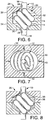
- the skewed coil contact 10 is placed within a through aperture 24 in a dielectric panel 26.
- the aperture 24 has openings 28 at both ends of a larger center section 30.
- the cross-sectional dimension of the center section 30 is slightly larger than the largest dimension of the contact perpendicular to the leads.
- the center section 30 has an oval cross section, where the direction 40 in which the coil 12 expands has the larger dimension.
- the smaller dimension 42 can be the same as the coil dimension, since the coil 12 does not expand in that dimension 42.
- the dielectric panel in contrast to what is shown in Fig. 6 , has a base sheet that contains one of the openings and the entire center section and a top sheet that contains only the other opening.
- the contact 10 is placed in the base sheet part of the aperture and the sheets are sandwiched together, capturing the contact 10 within the aperture.
- the dielectric panel 26 has two mirror image sheets 32, 34, where each sheet has one opening 28 and a half of the center section 30.
- the contact 10 is placed in one side of the aperture 24 and the sheets 32, 34 are sandwiched together, capturing the contact 10 within the aperture 24.
- the loops 14 of the coil 12 expand.
- the aperture 24 maintains the position of the contact 10 as it is compressed.
- the aperture 24 may also maintain the integrity of the contact 10 by preventing the coil loops 14 from separating under the axial compression.
- the skewed coil contact 10 is installed in the aperture 24 and the remaining space of the aperture 24 is filled with a compliant, electrically conductive elastomer 36, as shown in Fig. 8 .
- the elastomer 36 performs a dual function. It adds to the resiliency of the contact 10, meaning that the contact 10 can tolerate more operational cycles than without the elastomer 34.
- the elastomer 34 also aids in electrically shorting the coil loops 14, thus potentially minimizing the electrical parasitic values of the contact system.
- the skewed coil contact 10 can be made extremely small by employing extremely small wire and forming apertures 24 in the dielectric panel 26 for testing UUT's with pitches smaller that 0.5 mm (0.020").
- the contacts 10 are adaptable to silicon wafer probing with pitches in the micrometers.
- FIG. 9 An alternative arrangement of the contacts 10 within a dielectric panel 26 is shown in Fig. 9 . Note that one lead 16 is longer than the other 18 and that the apertures 24 are elongated and staggered. With this arrangement, the contacts 10 can be placed closer together. Particular applications of this arrangement include 4-wire testing where each IC lead requires two contacts, one for a drive current and the other for high-impedance sensing.
- the skewed coil contact can be made of an optical fiber so that it may be used to make a temporary connection to UUT's with fiber optic interfaces.
- the skewed coil leads protrude axially from the coil, thus directing the light signals straight in and out of the contact.
- the purpose is not to minimize parasitic electrical effects, since optical signals do not have such problems.
- the optical contact permits a mixture of electrical and optical signals on the same test fixture while providing the same compliance as the electrical skewed coil contact.
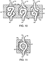
- the raveled wire type of contact which does not form part of the invention, shown in Figs. 10 and 11 , consists of a length of wire that is forced into a cylindrical cavity that has a diameter larger than the cross-sectional dimension of the wire, typically two to four times larger.
- the result shown variously in Figs. 10 and 11 , is a contact 50 that is comprised of randomly entangled convolutions 52 formed within the confines of a cylindrical shape with both extremities of the wire protruding paraxially as leads 54, 56 from either end of the convolutions 52.
- the leads 54, 56 protruding from the convolutions 52 provide a compliant contact point.
- the axially protruding leads 54, 56 are the key differentiators from the fuzz button contact of the prior art in that no additional contact elements are required in the contact system. Consequently, the contact has less inductance and can be made smaller than the fuzz button contact system.
- the wire can be made of the same materials as the skewed coil contact 10.
- a contact 50 using a rectangular cross-section wire can induce consistent convolutions 52.
- the wire When the wire is forced into a cavity at the time of manufacture, the wire tends to bend along its weakest point. With the rectangular cross-section, the weakest point is the shortest line through the wire axis, which is essentially the same throughout the length of the wire. Thus, a unidirectional collapse pattern is induced, causing the contact to compress consistently from contact to contact.
- the leads 54, 56 can be formed into shapes in the same manner as the leads 16, 18 of the skewed coil contact 10.
- the raveled wire contact 50 can be made very small, like the skewed coil contact 10.
- the raveled wire contact can be installed in a through aperture 58 in a dielectric panel 62.
- the remaining space of the aperture 58 can be filled with a compliant, conductive elastomer 60, as shown Fig. 11 .
- the cavity in which the contact 50 is formed can be round, square, or any other desired cross sectional shape. If the contact 50 is formed inside a rectangular, rather than circular, cavity, the apexes of the formed contact 50 may be used to hold the contact within the aperture 58.
Description
- The present invention relates to electrical contacts, more particularly, to very small compliant electrical contacts with very low inductance at high frequencies.
- The purpose of an electrical contact is to provide a separable electrical interconnection between two electrical conductors. The characteristic of separability means that the conductors are not interconnected by permanent mechanical means, such as soldering or bonding, but by temporary mechanical means. Consequently, in order to maintain a good mechanical contact in an attempt to minimize detrimental electrical effects of the contact, some form of spring force is used to press the two conductors together. These electrical contacts are called compliant (as in "flexible") contacts.
- Small compliant contacts are necessary for separably interconnecting integrated circuit (IC) devices to whatever electrical device the user desires. A prime example is connecting the IC to a test fixture or sorting equipment used for testing and sorting IC's during manufacture. The compliant contact should be as close to electrically transparent as possible in order to minimize parasitic effects, such as inductance, that alter the signals to and from the IC which could lead to erroneous results.
- Compliant contacts provide another advantage in that they can compensate for noncoplanarities of the electronic unit under test (UUT) being connected. The conduction points on the UUT are not exactly coplanar, that is, they are not within the same plane, even between the same conduction point on different UUT's. The compliant contacts deflect by different amounts depending upon the actual position of the conduction point.
- Conventional compliant contacts for connecting to UUT's include spring probes, conductive rubber, compliant beam contacts, and bunched up wire called fuzz buttons. Each technology provides the necessary means to overcome the noncoplanarities between the contact points and provides uniform electrical contact throughout a plurality of contacts. Each technology has shortcomings in one characteristic or another and all have high electrical parasitic characteristics. In addition, they are relatively expensive to manufacture.
- A typical spring probe consists of at least three or four parts, a hollow barrel with a spring and one or two plungers. The spring is housed in the barrel with the end of the plungers crimped in opposed open ends of the barrel at the ends of the spring. The spring biases the plungers outwardly, thereby providing a spring force to the tip of the plungers. Spring probes can have highly varying degrees of compliance and contact force, and are generally very reliable for making contact many times or for many cycles. Spring probes can accommodate many different conduction interfaces, such as pads, columns, balls, etc. Spring probes, however, have a size problem in that the spring itself cannot be made very small, otherwise consistent spring force from contact to contact cannot be maintained. Thus, spring probes are relatively large, leading to an unacceptably large inductance when used for electrical signals at higher frequencies. Additionally, spring probes are relatively costly since the three components must be manufactured separately and then assembled.
- Conductive rubber contacts are made of rubber and silicones of varying types with embedded conductive metal elements. These contact solutions usually are less inductive than spring probes, but have less compliance and are capable of fewer duty cycles than spring probes. The conductive rubber works when the conduction point is elevated off the UUT thus requiring a protruding feature from the UUT or the addition of a third conductive element to the system to act as a protruding member. This third member lessens the contact area for a given contact force and thus increases the force per unit area so that consistent contact can be made. The third element may be a screw machined button which rests on the rubber between the conduction point. This third element can only add inductance to the contact system.
- Compliant beam contacts are made of a conductive material formed such that deflection and contact force is attained at one end to the UUT conduction point while the other end remains fixed to the other conductor. In other words, the force is provided by one or more electrically conductive leaf springs. These contacts vary greatly in shape and application. Some compliant beam contacts are small enough to be used effectively with IC's. Some compliant beam contacts use another compliant material, such as rubber, to add to the compliance or contact force to the beam contact point. These later types tend to be smaller than traditional compliant beam contacts and thus have less inductance and are better suited for sorting higher frequency devices. However, these contacts still tend to be somewhat too large to be useful in some radio frequency (RF) applications.
- Fuzz buttons are a relatively old yet simple technology in which a wire is crumpled into a cylindrical shape. The resulting shape looks very much like tiny cylinder made of steel wool. When the cylinder is placed within a hole in a sheet of nonconductive material, it acts like a spring that is continuously electrically shorted. It provides a less inductive electrical path than other contact technologies. Like rubber contacts, the fuzz button is most commonly used with a third element needed to reach inside the hole of the nonconductive sheet to make contact with the fuzz button. This third element increases parasitic inductance, degrading the signals to and from the UUT.
- IC packaging technology is evolving toward being smaller, higher frequency (faster), and cheaper, resulting in new requirements for these types of electrical contacts. They need to perform adequately at the lowest cost.
- A compliant-coil type of contact is shown in
US 6174172 B1 . The coils compress along their axes. DocumentJP 2001/230035 A - An object of the present invention is to provide a compliant contact with a lower self-inductance at higher frequencies than existing technologies.
- Another object is to provide a low-self-inductance contact that provides sufficient compliance to test various UUT's.
- Yet another object is to provide a low-self-inductance contact that can be made extremely small for testing UUT's with close conduction points.
- A further object is to provide a low-self-inductance contact that is relatively inexpensive to manufacture.
- The present invention aims to provide a very low self-inductance, compliant contact and is defined in claim 1. Two types of contact may be identified. The skewed coil type includes a coil of wire with a pair of oppositely extending leads. The leads extend in a direction angled from the coil axis, the magnitude of the angle being dependent on the particular application. The greater the angle, the greater the force necessary to compress the contact. During compression, the coil loops are electrically shorted while they slide along each other. The coil only needs to have enough of a loop to cause a short circuit between the leads when compressed, a minimum of just over 360°.
- The cross-sectional shape of the wire can be any shape, including round, square, triangular, elliptical, rectangular, or star, nor does the cross-sectional dimension have to be uniform over the length of the wire. Cross-sections with flat sides provide a greater contact surface than wire with a round or oval cross-section, but are not necessarily preferred. The wire is made of any electrically conductive material which has inherent elastic properties.
- The lead ends can be configured in shapes that aid in the contact integrity, for example a hemisphere or ring for receiving a ball contact, or a spear for piercing oxides.
- In one application, the contact is placed within a through aperture in a dielectric panel. The aperture has openings at both ends of a larger center section. In one embodiment, the dielectric panel has a base sheet with one of the openings and the center section and a top sheet with the other opening. The contact is placed in the center section and the sheets are sandwiched together, capturing the contact within the aperture. In another embodiment, the dielectric panel has two mirror image sheets where each sheet has one opening and a half of the center section. The contact is placed in one side and the sheets are sandwiched together to capture the contact. Optionally, the remaining space of the aperture is filled with a compliant, electrically conductive elastomer that adds resiliency and aids in electrically shorting the coil loops.
- The raveled-wire type of contact, discussed by way of comparative example not forming part of the present invention, is created by forcing a length of wire into a cylindrical cavity that has a diameter larger than the cross-sectional dimension of the wire, resulting in randomly entangled convolutions formed within the confines of a cylindrical shape, the lead ends protruding paraxially from the convolutions. The characteristics of the wire are the same as those of the skewed coil contact. All other characteristics of the raveled wire contact are the same as or similar to those of the skewed coil contact.
- Other objects of the present invention will become apparent in the light of the following drawings and detailed description of the invention.
- For a fuller understanding of the nature and object of the present invention, reference is made to the accompanying drawings, wherein:
-
Fig. 1 is a perspective view of the basic contact of the skewed coil embodiment of the present invention; -
Fig. 2 is a side view of the skewed coil contact with oval loop s; -
Fig. 3 is a side view of the skewed coil contact made from a wire with rectangular cross-section; -
Fig. 4 is a perspective view of the skewed coil contact with a lead formed into a ring; -
Fig. 5 is a perspective view of the skewed coil contact with a lead formed into a prong; -
Fig. 6 is a partial cross-sectional side view of one embodiment of an assembly employing the skewed coil contact; -
Fig. 7 is a partial cross-sectional top view of the assembly ofFig. 6 ; -
Fig. 8 is a partial cross-sectional side view of another embodiment of an assembly employing the skewed coil contact and filled with a conductive elastomer; -
Fig. 9 is a partial cross-sectional side view of a pair of skewed coil contacts mounted in a dielectric sheet in very close proximity; -
Fig. 10 is a partial cross-sectional view of several configurations of the raveled wire contact mounted in a dielectric sheet; and -
Fig. 11 is a partial cross-sectional side view of a configuration of the raveled wire contact mounted in a dielectric sheet and filled with a conductive elastomer. - The present invention is a compliant electrical contact with a very low self-inductance. It has one embodiment.
- In the skewed coil embodiment, shown in
Figs. 1-9 , thecontact 10 is created by winding a length of electrically conductive wire into acylindrical coil 12. The gap betweenloops 14 of thecoil 12 ranges from essentially no gap (a closed coil) to a distance of up to about 100% of the largest wire cross-sectional dimension. The greater the wire cross-sectional dimension, the greater the gap can be as a percentage of the cross-sectional dimension. For example, with a wire cross-sectional dimension of 0.079 mm (0.0031 inch), a gap of 0.0025 mm (0.0001 inch) (3)% is acceptable, whereas with a wire cross-sectional dimension of 0.5 mm (0.020 inch), a gap of 0.25 mm (0.010 inch) (50%) is acceptable. - The
coil 12 can be round, as inFig. 1 , or oval, as inFig. 2 . The two wire extremities extend asleads coil 12 in opposite directions generally parallel to each other and at an angle from thecoil axis 38. The magnitude of this skew angle will depend on the particular application and the compliance forces required for that application. The greater the angle, the greater the force necessary to compress thecontact 10, which means that thecontact 10 will provide a greater force against the conduction point of the UUT. When thecontact 10 is mounted such that the leads 16, 18 can be compressed axially, thecoil 12 provides compliance as theloops 14 slide along each other. When the compression force is removed, theloops 14 return to their quiescent state. While compressed, thecoil 12 pushes theleads coil 14 provides the necessary feature of adjusting for the noncoplanarities of the conduction points. - Once the gap is closed, the
loops 14 are electrically shorted throughout the compression of thecontact 10 while they slide along each other. Thecoil 12 only needs to have enough of a loop to cause a short circuit between theleads coil 12 make contact during compression. - In addition to the skew angle, the force versus deflection curve of the skewed
coil contact 10 is also determined by the volume of the wire used in manufacturing the contact, e.g. the wire cross-sectional dimension, coil diameter, and wire length, as well as the cross-sectional shape and wire material. The cross-sectional shape of the wire can be round, as shown inFig. 1 , or any other shape including square, triangular, elliptical, rectangular, or star. The present invention also contemplates that the cross-sectional dimension does not have to be uniform over the length of the wire. When using wire with a cross-section having flat sides, such as rectangular or star-shaped, adjacent loops are in contact along a greater surface area than when using wire with a round or oval cross-section. Consequently, the shortest electrical path possible is created, resulting in a lower inductance connection. However, for cost and other reasons, wire with flat sides is not necessarily preferred over round and oval wire. - The wire can be made of any electrically conductive material which has inherent elastic properties, for example, stainless steel, beryllium copper, copper, brass, and nickel chromium alloy. All of these materials can be used in varying degrees of temper from annealed to fully hardened.
- The ends of the
leads ring 20, shown inFig. 4 , for receiving a ball contact as in the testing of a ball grid array (BGA) device. Another example is a spear, shown inFig. 5 , with one ormore prongs 22 for piercing oxides at the conduction point. - In one application, shown in
Fig. 6 , the skewedcoil contact 10 is placed within a throughaperture 24 in adielectric panel 26. Theaperture 24 hasopenings 28 at both ends of alarger center section 30. The cross-sectional dimension of thecenter section 30 is slightly larger than the largest dimension of the contact perpendicular to the leads. As shown in top view inFig. 7 , thecenter section 30 has an oval cross section, where thedirection 40 in which thecoil 12 expands has the larger dimension. Thesmaller dimension 42 can be the same as the coil dimension, since thecoil 12 does not expand in thatdimension 42. - In one embodiment, in contrast to what is shown in
Fig. 6 , the dielectric panel has a base sheet that contains one of the openings and the entire center section and a top sheet that contains only the other opening. Thecontact 10 is placed in the base sheet part of the aperture and the sheets are sandwiched together, capturing thecontact 10 within the aperture. - In other embodiments, as shown in
Figs. 6 and 8 , thedielectric panel 26 has twomirror image sheets opening 28 and a half of thecenter section 30. Thecontact 10 is placed in one side of theaperture 24 and thesheets contact 10 within theaperture 24. - When an axial compression force is applied to the
leads openings 28 of thedielectric panel 26, theloops 14 of thecoil 12 expand. Theaperture 24 maintains the position of thecontact 10 as it is compressed. Theaperture 24 may also maintain the integrity of thecontact 10 by preventing thecoil loops 14 from separating under the axial compression. - In another variant, the skewed
coil contact 10 is installed in theaperture 24 and the remaining space of theaperture 24 is filled with a compliant, electricallyconductive elastomer 36, as shown inFig. 8 . Theelastomer 36 performs a dual function. It adds to the resiliency of thecontact 10, meaning that thecontact 10 can tolerate more operational cycles than without theelastomer 34. Theelastomer 34 also aids in electrically shorting thecoil loops 14, thus potentially minimizing the electrical parasitic values of the contact system. - The skewed
coil contact 10 can be made extremely small by employing extremely small wire and formingapertures 24 in thedielectric panel 26 for testing UUT's with pitches smaller that 0.5 mm (0.020"). Thecontacts 10 are adaptable to silicon wafer probing with pitches in the micrometers. - An alternative arrangement of the
contacts 10 within adielectric panel 26 is shown inFig. 9 . Note that onelead 16 is longer than the other 18 and that theapertures 24 are elongated and staggered. With this arrangement, thecontacts 10 can be placed closer together. Particular applications of this arrangement include 4-wire testing where each IC lead requires two contacts, one for a drive current and the other for high-impedance sensing. - According to a further possible development not forming part of the present invention, the skewed coil contact can be made of an optical fiber so that it may be used to make a temporary connection to UUT's with fiber optic interfaces. The skewed coil leads protrude axially from the coil, thus directing the light signals straight in and out of the contact. The purpose, obviously, is not to minimize parasitic electrical effects, since optical signals do not have such problems. The optical contact permits a mixture of electrical and optical signals on the same test fixture while providing the same compliance as the electrical skewed coil contact.
- The raveled wire type of contact which does not form part of the invention, shown in
Figs. 10 and 11 , consists of a length of wire that is forced into a cylindrical cavity that has a diameter larger than the cross-sectional dimension of the wire, typically two to four times larger. The result, shown variously inFigs. 10 and 11 , is acontact 50 that is comprised of randomly entangledconvolutions 52 formed within the confines of a cylindrical shape with both extremities of the wire protruding paraxially as leads 54, 56 from either end of theconvolutions 52. The leads 54, 56 protruding from theconvolutions 52 provide a compliant contact point. The axially protruding leads 54, 56 are the key differentiators from the fuzz button contact of the prior art in that no additional contact elements are required in the contact system. Consequently, the contact has less inductance and can be made smaller than the fuzz button contact system. - The wire can be made of the same materials as the skewed
coil contact 10. Acontact 50 using a rectangular cross-section wire can induceconsistent convolutions 52. When the wire is forced into a cavity at the time of manufacture, the wire tends to bend along its weakest point. With the rectangular cross-section, the weakest point is the shortest line through the wire axis, which is essentially the same throughout the length of the wire. Thus, a unidirectional collapse pattern is induced, causing the contact to compress consistently from contact to contact. - The leads 54, 56 can be formed into shapes in the same manner as the
leads coil contact 10. The raveledwire contact 50 can be made very small, like the skewedcoil contact 10. As with the skewedcoil contact 10, the raveled wire contact can be installed in a throughaperture 58 in adielectric panel 62. Also, as with the skewedcoil contact 10, the remaining space of theaperture 58 can be filled with a compliant,conductive elastomer 60, as shownFig. 11 . - The cavity in which the
contact 50 is formed can be round, square, or any other desired cross sectional shape. If thecontact 50 is formed inside a rectangular, rather than circular, cavity, the apexes of the formedcontact 50 may be used to hold the contact within theaperture 58.
Claims (7)
- A compliant electrical contact (10) comprising a length of wire having extremities (16, 18) and being composed of an electrically conductive, inherently elastic material; wherein(a) the wire is formed into a coil (12) having at least slightly more than one loop (14) and an axis (38);(b) the extremities of the wire extend from the coil at a bent portion as straight leads (16, 18) in approximately opposite directions; and characterized in that(c) the coil axis (38) is at a skew angle with respect to the leads (16, 18), so that, once any gap between the loops (14) of the coil (12) is closed by an axial compression of the leads (16, 18), the loops (14) remain electrically shorted throughout compression.
- A compliant electrical contact (10) according to claim 1, wherein at least one of the leads (16, 18) is configured with a shaped end.
- A compliant electrical contact (10) according to claim 1 or 2, wherein the wire is metallic.
- A compliant electrical contact (10) according to any preceding claim, wherein the gap between the loops (14) of the wire is no more than 100% of the cross-sectional dimension of the wire.
- A compliant electrical contact assembly comprising:at least one compliant electrical contact (10) according to any preceding claim; anda dielectric panel (26) having a through-aperture (24) for each such electrical contact (10), this through-aperture (24) having a center section (30) in which the coil (12) is captured and opposed openings (28) through which the leads (16, 18) extend, the center section (30) being of a size permitting the coil (12) to contract and expand as pressure is applied axially to and removed from the leads.
- A compliant electrical contact assembly according to claim 5, wherein the aperture (24) is filled with a compliant, conductive elastomer (36) surrounding the contact.
- A compliant electrical contact assembly according to claim 5 or 6, wherein the axis (38) of the coil is skewed with respect to the normal to the dielectric panel (26).
Applications Claiming Priority (5)
| Application Number | Priority Date | Filing Date | Title |
|---|---|---|---|
| US34985002P | 2002-01-17 | 2002-01-17 | |
| US34985202P | 2002-01-17 | 2002-01-17 | |
| US349850P | 2002-01-17 | ||
| US349852P | 2002-01-17 | ||
| PCT/US2003/001035 WO2003063201A2 (en) | 2002-01-17 | 2003-01-14 | Compliant electrical contact |
Publications (3)
| Publication Number | Publication Date |
|---|---|
| EP1474822A2 EP1474822A2 (en) | 2004-11-10 |
| EP1474822A4 EP1474822A4 (en) | 2007-03-14 |
| EP1474822B1 true EP1474822B1 (en) | 2016-12-07 |
Family
ID=27616754
Family Applications (1)
| Application Number | Title | Priority Date | Filing Date |
|---|---|---|---|
| EP03731913.4A Expired - Lifetime EP1474822B1 (en) | 2002-01-17 | 2003-01-14 | Compliant electrical contact |
Country Status (8)
| Country | Link |
|---|---|
| US (1) | US6787709B2 (en) |
| EP (1) | EP1474822B1 (en) |
| JP (2) | JP2005516344A (en) |
| KR (1) | KR100874541B1 (en) |
| CN (1) | CN1315135C (en) |
| CA (1) | CA2473726A1 (en) |
| IL (1) | IL163071A (en) |
| WO (1) | WO2003063201A2 (en) |
Cited By (3)
| Publication number | Priority date | Publication date | Assignee | Title |
|---|---|---|---|---|
| US10784553B2 (en) | 2018-09-07 | 2020-09-22 | International Business Machines Corporation | Well thermalized stripline formation for high-density connections in quantum applications |
| US10891251B2 (en) | 2018-11-09 | 2021-01-12 | International Business Machines Corporation | Signal connector for microwave circuits |
| US11551125B2 (en) | 2019-02-21 | 2023-01-10 | International Business Machines Corporation | High density microwave hermetic interconnects for quantum applications |
Families Citing this family (17)
| Publication number | Priority date | Publication date | Assignee | Title |
|---|---|---|---|---|
| US6909056B2 (en) * | 2002-01-17 | 2005-06-21 | Ardent Concepts, Inc. | Compliant electrical contact assembly |
| US7446545B2 (en) * | 2003-05-08 | 2008-11-04 | Unitechno Inc. | Anisotropically conductive sheet |
| US20040224148A1 (en) * | 2003-05-08 | 2004-11-11 | Hitoshi Matsunaga | Anisotropically conductive sheet |
| US6981879B2 (en) * | 2004-03-18 | 2006-01-03 | International Business Machines Corporation | Land grid array (LGA) interposer with adhesive-retained contacts and method of manufacture |
| US7402051B1 (en) * | 2005-11-10 | 2008-07-22 | Antares Advanced Test Technologies, Inc. | Interconnect assembly for testing integrated circuit packages |
| JP2008027759A (en) * | 2006-07-21 | 2008-02-07 | Fujikura Ltd | Ic socket and ic package mounting device |
| JP2009002845A (en) * | 2007-06-22 | 2009-01-08 | Micronics Japan Co Ltd | Contact and connection apparatus |
| EP2206197B1 (en) * | 2007-10-29 | 2016-09-21 | Ardent Concepts, Inc. | Compliant electrical contact and assembly comprising the same |
| USRE46958E1 (en) | 2011-10-24 | 2018-07-17 | Ardent Concepts, Inc. | Controlled-impedance cable termination using compliant interconnect elements |
| USRE47459E1 (en) | 2011-10-24 | 2019-06-25 | Ardent Concepts, Inc. | Controlled-impedance cable termination using compliant interconnect elements |
| GB2498536B (en) * | 2012-01-17 | 2016-03-09 | Control Tech Ltd | Electrical assembly |
| JP6071633B2 (en) * | 2013-02-25 | 2017-02-01 | 秀雄 西川 | Contact, inspection jig, and method of manufacturing contact |
| JP2014178175A (en) * | 2013-03-14 | 2014-09-25 | Micronics Japan Co Ltd | Interconnection device and assembling method of interconnection device |
| DE102016006774A1 (en) * | 2016-06-02 | 2017-12-07 | Rosenberger Hochfrequenztechnik Gmbh & Co. Kg | contacting arrangement |
| US10790432B2 (en) | 2018-07-27 | 2020-09-29 | International Business Machines Corporation | Cryogenic device with multiple transmission lines and microwave attenuators |
| US10931040B1 (en) * | 2018-08-02 | 2021-02-23 | Ardent Concepts, Inc. | Controlled-impedance circuit board connector assembly |
| KR102582793B1 (en) * | 2021-08-02 | 2023-09-26 | 주식회사 아이에스시 | Testor socket and manufacturing method thereof |
Citations (2)
| Publication number | Priority date | Publication date | Assignee | Title |
|---|---|---|---|---|
| US5993269A (en) * | 1996-12-25 | 1999-11-30 | Nec Corporation | Connecting pin having electrically conductive magnetic fluid |
| JP2001230035A (en) * | 2000-02-17 | 2001-08-24 | Kasasaku Electronics:Kk | Ic socket |
Family Cites Families (18)
| Publication number | Priority date | Publication date | Assignee | Title |
|---|---|---|---|---|
| FR959460A (en) * | 1950-03-30 | |||
| US4029375A (en) * | 1976-06-14 | 1977-06-14 | Electronic Engineering Company Of California | Miniature electrical connector |
| EP0385142B1 (en) * | 1989-02-28 | 1995-09-27 | Fujitsu Limited | Electrical connecting apparatus |
| US4998886A (en) * | 1989-07-07 | 1991-03-12 | Teledyne Kinetics | High density stacking connector |
| EP0462706A1 (en) * | 1990-06-11 | 1991-12-27 | ITT INDUSTRIES, INC. (a Delaware corporation) | Contact assembly |
| EP0555368B1 (en) * | 1990-10-29 | 1999-04-14 | General DataComm, Inc. | Electrical connectors having tapered spring contact element |
| US5101553A (en) * | 1991-04-29 | 1992-04-07 | Microelectronics And Computer Technology Corporation | Method of making a metal-on-elastomer pressure contact connector |
| US5167512A (en) * | 1991-07-05 | 1992-12-01 | Walkup William B | Multi-chip module connector element and system |
| US5230632A (en) * | 1991-12-19 | 1993-07-27 | International Business Machines Corporation | Dual element electrical contact and connector assembly utilizing same |
| GB2273830B (en) * | 1992-12-24 | 1997-04-16 | Whitaker Corp | Electrical contact elements for interposer structures |
| EP0616394A1 (en) * | 1993-03-16 | 1994-09-21 | Hewlett-Packard Company | Method and system for producing electrically interconnected circuits |
| US5427535A (en) * | 1993-09-24 | 1995-06-27 | Aries Electronics, Inc. | Resilient electrically conductive terminal assemblies |
| US5495667A (en) * | 1994-11-07 | 1996-03-05 | Micron Technology, Inc. | Method for forming contact pins for semiconductor dice and interconnects |
| US5667410A (en) * | 1995-11-21 | 1997-09-16 | Everett Charles Technologies, Inc. | One-piece compliant probe |
| JP3653131B2 (en) * | 1995-12-28 | 2005-05-25 | 日本発条株式会社 | Conductive contact |
| CN1255686C (en) * | 1996-04-12 | 2006-05-10 | 日本发条株式会社 | Conductive contact unit system |
| JP4060919B2 (en) * | 1997-11-28 | 2008-03-12 | 富士通株式会社 | Electrical connection device, contact manufacturing method, and semiconductor test method |
| US6114240A (en) * | 1997-12-18 | 2000-09-05 | Micron Technology, Inc. | Method for fabricating semiconductor components using focused laser beam |
-
2003
- 2003-01-14 WO PCT/US2003/001035 patent/WO2003063201A2/en active Application Filing
- 2003-01-14 CN CNB038023563A patent/CN1315135C/en not_active Expired - Lifetime
- 2003-01-14 US US10/341,723 patent/US6787709B2/en not_active Expired - Lifetime
- 2003-01-14 JP JP2003562968A patent/JP2005516344A/en active Pending
- 2003-01-14 EP EP03731913.4A patent/EP1474822B1/en not_active Expired - Lifetime
- 2003-01-14 CA CA002473726A patent/CA2473726A1/en not_active Abandoned
- 2003-01-14 KR KR1020047011112A patent/KR100874541B1/en active IP Right Grant
-
2004
- 2004-07-15 IL IL163071A patent/IL163071A/en not_active IP Right Cessation
-
2009
- 2009-04-20 JP JP2009101625A patent/JP4886001B2/en not_active Expired - Lifetime
Patent Citations (2)
| Publication number | Priority date | Publication date | Assignee | Title |
|---|---|---|---|---|
| US5993269A (en) * | 1996-12-25 | 1999-11-30 | Nec Corporation | Connecting pin having electrically conductive magnetic fluid |
| JP2001230035A (en) * | 2000-02-17 | 2001-08-24 | Kasasaku Electronics:Kk | Ic socket |
Cited By (4)
| Publication number | Priority date | Publication date | Assignee | Title |
|---|---|---|---|---|
| US10784553B2 (en) | 2018-09-07 | 2020-09-22 | International Business Machines Corporation | Well thermalized stripline formation for high-density connections in quantum applications |
| US10891251B2 (en) | 2018-11-09 | 2021-01-12 | International Business Machines Corporation | Signal connector for microwave circuits |
| US11551125B2 (en) | 2019-02-21 | 2023-01-10 | International Business Machines Corporation | High density microwave hermetic interconnects for quantum applications |
| US11900217B2 (en) | 2019-02-21 | 2024-02-13 | International Business Machines Corporation | High density microwave hermetic interconnects for quantum applications |
Also Published As
| Publication number | Publication date |
|---|---|
| US6787709B2 (en) | 2004-09-07 |
| WO2003063201A2 (en) | 2003-07-31 |
| EP1474822A4 (en) | 2007-03-14 |
| CA2473726A1 (en) | 2003-07-31 |
| JP2005516344A (en) | 2005-06-02 |
| CN1315135C (en) | 2007-05-09 |
| US20030132020A1 (en) | 2003-07-17 |
| EP1474822A2 (en) | 2004-11-10 |
| IL163071A (en) | 2009-11-18 |
| KR20040103916A (en) | 2004-12-09 |
| JP4886001B2 (en) | 2012-02-29 |
| WO2003063201A3 (en) | 2003-10-16 |
| KR100874541B1 (en) | 2008-12-16 |
| JP2009164135A (en) | 2009-07-23 |
| CN1618107A (en) | 2005-05-18 |
Similar Documents
| Publication | Publication Date | Title |
|---|---|---|
| EP1474822B1 (en) | Compliant electrical contact | |
| US7019222B2 (en) | Compliant electrical contact assembly | |
| US7126062B1 (en) | Compliant electrical contact assembly | |
| EP1741111A1 (en) | Compliant electrical contact assembly | |
| JP4585024B2 (en) | Electrical contact probe with flexible internal interconnect | |
| EP2206197B1 (en) | Compliant electrical contact and assembly comprising the same | |
| EP2646839B1 (en) | Compliant electrical contact and assembly | |
| US6264508B1 (en) | Female type contact piece enabling electrical contact with a male element | |
| KR100562602B1 (en) | Press contact clamping connector and its connection structure | |
| CN110581085B (en) | Integrated spring needle | |
| JP2005516344A5 (en) | ||
| KR101894965B1 (en) | Probe pin and ic socket | |
| USRE41663E1 (en) | Compliant electrical contact assembly | |
| CN111293448A (en) | Integrated spring needle with pressure welding structure | |
| US20060267620A1 (en) | Interconnecting apparatus and a contact element therefor |
Legal Events
| Date | Code | Title | Description |
|---|---|---|---|
| PUAI | Public reference made under article 153(3) epc to a published international application that has entered the european phase |
Free format text: ORIGINAL CODE: 0009012 |
|
| 17P | Request for examination filed |
Effective date: 20040811 |
|
| AK | Designated contracting states |
Kind code of ref document: A2 Designated state(s): AT BE BG CH CY CZ DE DK EE ES FI FR GB GR HU IE IT LI LU MC NL PT SE SI SK TR |
|
| AX | Request for extension of the european patent |
Extension state: AL LT LV MK RO |
|
| RAP1 | Party data changed (applicant data changed or rights of an application transferred) |
Owner name: ARDENT CONCEPTS, INC. |
|
| A4 | Supplementary search report drawn up and despatched |
Effective date: 20070212 |
|
| RIC1 | Information provided on ipc code assigned before grant |
Ipc: H01R 13/24 20060101AFI20070206BHEP Ipc: H01R 13/33 20060101ALN20070206BHEP |
|
| 17Q | First examination report despatched |
Effective date: 20100920 |
|
| GRAP | Despatch of communication of intention to grant a patent |
Free format text: ORIGINAL CODE: EPIDOSNIGR1 |
|
| INTG | Intention to grant announced |
Effective date: 20160426 |
|
| GRAS | Grant fee paid |
Free format text: ORIGINAL CODE: EPIDOSNIGR3 |
|
| GRAJ | Information related to disapproval of communication of intention to grant by the applicant or resumption of examination proceedings by the epo deleted |
Free format text: ORIGINAL CODE: EPIDOSDIGR1 |
|
| GRAL | Information related to payment of fee for publishing/printing deleted |
Free format text: ORIGINAL CODE: EPIDOSDIGR3 |
|
| INTC | Intention to grant announced (deleted) | ||
| GRAR | Information related to intention to grant a patent recorded |
Free format text: ORIGINAL CODE: EPIDOSNIGR71 |
|
| GRAA | (expected) grant |
Free format text: ORIGINAL CODE: 0009210 |
|
| INTG | Intention to grant announced |
Effective date: 20161027 |
|
| AK | Designated contracting states |
Kind code of ref document: B1 Designated state(s): AT BE BG CH CY CZ DE DK EE ES FI FR GB GR HU IE IT LI LU MC NL PT SE SI SK TR |
|
| REG | Reference to a national code |
Ref country code: GB Ref legal event code: FG4D |
|
| RAP2 | Party data changed (patent owner data changed or rights of a patent transferred) |
Owner name: ARDENT CONCEPTS, INC. |
|
| REG | Reference to a national code |
Ref country code: CH Ref legal event code: EP Ref country code: AT Ref legal event code: REF Ref document number: 852457 Country of ref document: AT Kind code of ref document: T Effective date: 20161215 |
|
| REG | Reference to a national code |
Ref country code: IE Ref legal event code: FG4D |
|
| REG | Reference to a national code |
Ref country code: DE Ref legal event code: R096 Ref document number: 60349685 Country of ref document: DE |
|
| REG | Reference to a national code |
Ref country code: FR Ref legal event code: PLFP Year of fee payment: 15 |
|
| REG | Reference to a national code |
Ref country code: NL Ref legal event code: MP Effective date: 20161207 |
|
| PG25 | Lapsed in a contracting state [announced via postgrant information from national office to epo] |
Ref country code: SE Free format text: LAPSE BECAUSE OF FAILURE TO SUBMIT A TRANSLATION OF THE DESCRIPTION OR TO PAY THE FEE WITHIN THE PRESCRIBED TIME-LIMIT Effective date: 20161207 Ref country code: GR Free format text: LAPSE BECAUSE OF FAILURE TO SUBMIT A TRANSLATION OF THE DESCRIPTION OR TO PAY THE FEE WITHIN THE PRESCRIBED TIME-LIMIT Effective date: 20170308 |
|
| REG | Reference to a national code |
Ref country code: AT Ref legal event code: MK05 Ref document number: 852457 Country of ref document: AT Kind code of ref document: T Effective date: 20161207 |
|
| PG25 | Lapsed in a contracting state [announced via postgrant information from national office to epo] |
Ref country code: ES Free format text: LAPSE BECAUSE OF FAILURE TO SUBMIT A TRANSLATION OF THE DESCRIPTION OR TO PAY THE FEE WITHIN THE PRESCRIBED TIME-LIMIT Effective date: 20161207 Ref country code: BE Free format text: LAPSE BECAUSE OF NON-PAYMENT OF DUE FEES Effective date: 20170131 Ref country code: FI Free format text: LAPSE BECAUSE OF FAILURE TO SUBMIT A TRANSLATION OF THE DESCRIPTION OR TO PAY THE FEE WITHIN THE PRESCRIBED TIME-LIMIT Effective date: 20161207 |
|
| PG25 | Lapsed in a contracting state [announced via postgrant information from national office to epo] |
Ref country code: NL Free format text: LAPSE BECAUSE OF FAILURE TO SUBMIT A TRANSLATION OF THE DESCRIPTION OR TO PAY THE FEE WITHIN THE PRESCRIBED TIME-LIMIT Effective date: 20161207 |
|
| PG25 | Lapsed in a contracting state [announced via postgrant information from national office to epo] |
Ref country code: SK Free format text: LAPSE BECAUSE OF FAILURE TO SUBMIT A TRANSLATION OF THE DESCRIPTION OR TO PAY THE FEE WITHIN THE PRESCRIBED TIME-LIMIT Effective date: 20161207 Ref country code: EE Free format text: LAPSE BECAUSE OF FAILURE TO SUBMIT A TRANSLATION OF THE DESCRIPTION OR TO PAY THE FEE WITHIN THE PRESCRIBED TIME-LIMIT Effective date: 20161207 Ref country code: CZ Free format text: LAPSE BECAUSE OF FAILURE TO SUBMIT A TRANSLATION OF THE DESCRIPTION OR TO PAY THE FEE WITHIN THE PRESCRIBED TIME-LIMIT Effective date: 20161207 |
|
| PG25 | Lapsed in a contracting state [announced via postgrant information from national office to epo] |
Ref country code: BE Free format text: LAPSE BECAUSE OF FAILURE TO SUBMIT A TRANSLATION OF THE DESCRIPTION OR TO PAY THE FEE WITHIN THE PRESCRIBED TIME-LIMIT Effective date: 20161207 Ref country code: PT Free format text: LAPSE BECAUSE OF FAILURE TO SUBMIT A TRANSLATION OF THE DESCRIPTION OR TO PAY THE FEE WITHIN THE PRESCRIBED TIME-LIMIT Effective date: 20170407 Ref country code: AT Free format text: LAPSE BECAUSE OF FAILURE TO SUBMIT A TRANSLATION OF THE DESCRIPTION OR TO PAY THE FEE WITHIN THE PRESCRIBED TIME-LIMIT Effective date: 20161207 Ref country code: BG Free format text: LAPSE BECAUSE OF FAILURE TO SUBMIT A TRANSLATION OF THE DESCRIPTION OR TO PAY THE FEE WITHIN THE PRESCRIBED TIME-LIMIT Effective date: 20170307 |
|
| REG | Reference to a national code |
Ref country code: CH Ref legal event code: PL |
|
| REG | Reference to a national code |
Ref country code: DE Ref legal event code: R097 Ref document number: 60349685 Country of ref document: DE |
|
| PG25 | Lapsed in a contracting state [announced via postgrant information from national office to epo] |
Ref country code: MC Free format text: LAPSE BECAUSE OF FAILURE TO SUBMIT A TRANSLATION OF THE DESCRIPTION OR TO PAY THE FEE WITHIN THE PRESCRIBED TIME-LIMIT Effective date: 20161207 |
|
| PLBE | No opposition filed within time limit |
Free format text: ORIGINAL CODE: 0009261 |
|
| STAA | Information on the status of an ep patent application or granted ep patent |
Free format text: STATUS: NO OPPOSITION FILED WITHIN TIME LIMIT |
|
| PG25 | Lapsed in a contracting state [announced via postgrant information from national office to epo] |
Ref country code: LI Free format text: LAPSE BECAUSE OF NON-PAYMENT OF DUE FEES Effective date: 20170131 Ref country code: CH Free format text: LAPSE BECAUSE OF NON-PAYMENT OF DUE FEES Effective date: 20170131 |
|
| REG | Reference to a national code |
Ref country code: IE Ref legal event code: MM4A |
|
| 26N | No opposition filed |
Effective date: 20170908 |
|
| PG25 | Lapsed in a contracting state [announced via postgrant information from national office to epo] |
Ref country code: LU Free format text: LAPSE BECAUSE OF NON-PAYMENT OF DUE FEES Effective date: 20170114 Ref country code: DK Free format text: LAPSE BECAUSE OF FAILURE TO SUBMIT A TRANSLATION OF THE DESCRIPTION OR TO PAY THE FEE WITHIN THE PRESCRIBED TIME-LIMIT Effective date: 20161207 Ref country code: SI Free format text: LAPSE BECAUSE OF FAILURE TO SUBMIT A TRANSLATION OF THE DESCRIPTION OR TO PAY THE FEE WITHIN THE PRESCRIBED TIME-LIMIT Effective date: 20161207 |
|
| REG | Reference to a national code |
Ref country code: FR Ref legal event code: PLFP Year of fee payment: 16 |
|
| PG25 | Lapsed in a contracting state [announced via postgrant information from national office to epo] |
Ref country code: IE Free format text: LAPSE BECAUSE OF NON-PAYMENT OF DUE FEES Effective date: 20170114 |
|
| PG25 | Lapsed in a contracting state [announced via postgrant information from national office to epo] |
Ref country code: HU Free format text: LAPSE BECAUSE OF FAILURE TO SUBMIT A TRANSLATION OF THE DESCRIPTION OR TO PAY THE FEE WITHIN THE PRESCRIBED TIME-LIMIT; INVALID AB INITIO Effective date: 20030114 |
|
| PG25 | Lapsed in a contracting state [announced via postgrant information from national office to epo] |
Ref country code: CY Free format text: LAPSE BECAUSE OF NON-PAYMENT OF DUE FEES Effective date: 20161207 |
|
| PG25 | Lapsed in a contracting state [announced via postgrant information from national office to epo] |
Ref country code: TR Free format text: LAPSE BECAUSE OF FAILURE TO SUBMIT A TRANSLATION OF THE DESCRIPTION OR TO PAY THE FEE WITHIN THE PRESCRIBED TIME-LIMIT Effective date: 20161207 |
|
| REG | Reference to a national code |
Ref country code: DE Ref legal event code: R082 Ref document number: 60349685 Country of ref document: DE Representative=s name: HL KEMPNER PATENTANWALT, RECHTSANWALT, SOLICIT, DE |
|
| PGFP | Annual fee paid to national office [announced via postgrant information from national office to epo] |
Ref country code: GB Payment date: 20220126 Year of fee payment: 20 Ref country code: DE Payment date: 20220131 Year of fee payment: 20 |
|
| PGFP | Annual fee paid to national office [announced via postgrant information from national office to epo] |
Ref country code: IT Payment date: 20220121 Year of fee payment: 20 Ref country code: FR Payment date: 20220121 Year of fee payment: 20 |
|
| REG | Reference to a national code |
Ref country code: DE Ref legal event code: R071 Ref document number: 60349685 Country of ref document: DE |
|
| REG | Reference to a national code |
Ref country code: GB Ref legal event code: PE20 Expiry date: 20230113 |
|
| PG25 | Lapsed in a contracting state [announced via postgrant information from national office to epo] |
Ref country code: GB Free format text: LAPSE BECAUSE OF EXPIRATION OF PROTECTION Effective date: 20230113 |