EP1473927A1 - Procédé d'échantillonnage du signal délivré par un pixel actif d'un capteur d'image, et capteur correspondant - Google Patents
Procédé d'échantillonnage du signal délivré par un pixel actif d'un capteur d'image, et capteur correspondant Download PDFInfo
- Publication number
- EP1473927A1 EP1473927A1 EP04290772A EP04290772A EP1473927A1 EP 1473927 A1 EP1473927 A1 EP 1473927A1 EP 04290772 A EP04290772 A EP 04290772A EP 04290772 A EP04290772 A EP 04290772A EP 1473927 A1 EP1473927 A1 EP 1473927A1
- Authority
- EP
- European Patent Office
- Prior art keywords
- sampling
- duration
- follower transistor
- bias current
- predetermined
- Prior art date
- Legal status (The legal status is an assumption and is not a legal conclusion. Google has not performed a legal analysis and makes no representation as to the accuracy of the status listed.)
- Granted
Links
Images


Classifications
-
- H—ELECTRICITY
- H04—ELECTRIC COMMUNICATION TECHNIQUE
- H04N—PICTORIAL COMMUNICATION, e.g. TELEVISION
- H04N25/00—Circuitry of solid-state image sensors [SSIS]; Control thereof
- H04N25/60—Noise processing, e.g. detecting, correcting, reducing or removing noise
- H04N25/616—Noise processing, e.g. detecting, correcting, reducing or removing noise involving a correlated sampling function, e.g. correlated double sampling [CDS] or triple sampling
-
- H—ELECTRICITY
- H04—ELECTRIC COMMUNICATION TECHNIQUE
- H04N—PICTORIAL COMMUNICATION, e.g. TELEVISION
- H04N25/00—Circuitry of solid-state image sensors [SSIS]; Control thereof
- H04N25/70—SSIS architectures; Circuits associated therewith
- H04N25/76—Addressed sensors, e.g. MOS or CMOS sensors
- H04N25/78—Readout circuits for addressed sensors, e.g. output amplifiers or A/D converters
Definitions
- the invention relates to the processing of signals delivered by a pixel array of an image sensor, and, more particularly, improving the dynamic and noise performance of the sampling signal from a matrix of active pixels produced in CMOS technology.
- An image sensor conventionally comprises a matrix of pixels. Each pixel delivers an electrical signal, the level of which depends of the amount of light received by the pixel. This signal is stored conventionally in a pair of sampling capacitors then there is for example amplified in a sense amplifier.
- the passage of the bias current in the pixel follower transistor causes white noise, the band of which bandwidth is limited by the transistor impedance and the total capacity of the sampling capacitor (for example of the order of 0.5 pF) and the column (bit line) (for example of the order of 1pF).
- this current is sized for speed and precision constraints, and it is typically of the order of 1 microampere, which allows sampling in about a microsecond.
- the current source also participates in white noise.
- this white noise has an average value estimated at 150 approximately microvolts.
- the usable signal range is all the more limited that the gate-source voltage of the follower transistor is large.
- the grid-source voltage is related to the square root of the ratio between the current of the follower transistor and a coefficient depending on technological characteristics of the transistor.
- this technological coefficient does not can hardly be increased in practice.
- the invention aims to improve this problem.
- the object of the invention is to reduce the sampling noise.
- the invention also aims to reduce the gate-source voltage of the follower transistor so as to exploit more useful signal without clipping.
- the invention therefore proposes a signal sampling method delivered by an active pixel of an image sensor, this method comprising a signal storage phase in a pair of capacitors with two effective electrical connections successive successive of two sampling capacitors with the pixel follower transistor during two sampling pulses respective corresponding respectively to two pixel voltage levels different successives applied to the gate of the follower transistor.
- the bias current is cut. Therefore, the gate-source voltage becomes equal to first order at the threshold voltage of the follower transistor. There are by therefore less gate-source voltage, which allows more useful signal without clipping. In addition, the contributions of white noise due to this bias current disappear with the latter and it consequently a reduced sampling noise ensues.
- the voltage variation in the bit line is positive and the current necessary to produce this variation goes through the follower transistor.
- This current is very low and the follower transistor is polarized in weak inversion.
- the noise band is very reduced and the noise spectral density presents a more amplitude low, resulting in a considerable improvement in noise.
- the second duration is advantageously chosen so as to obtain at the end of each sampling pulse, a residual current flowing in the follower transistor below a predetermined threshold corresponding to a predetermined threshold level of transistor noise follower.
- the predetermined threshold level for the noise of the follower transistor is between approximately 50 and 100 microvolts.
- the first duration is advantageously a fraction of the duration of said sampling pulse, the bias current then being greater than a predetermined threshold.
- the first duration can be of the order of 100 nanoseconds and the bias current, on the order of 10 microamperes. This allows, using a current about 10 to 20 times greater than a bias current used in the prior art, to achieve stabilization all the faster for the state of charge of each sampling capacitor.
- the voltages reached on the sampling capacitors depend only on the two levels of different pixel voltage. The principle is therefore deterministic.
- the strong current advantageously used before breaking, is a element which contributes to obtaining this deterministic principle.
- each capacitor sampling it is advantageous to preload to a predetermined initial value before each sampling pulse.
- Preload allows you to start each sampling from a deterministic state. Indeed, from then on that the current is cut, the final tension towards which one tends depends of the initial tension. Preload allows you to lose all "memory" of the voltage sampled in the previous cycle.
- the invention also provides an image sensor comprising a matrix of active pixels, and means for processing information delivered by said matrix of active pixels, the processing means with one pair of sampling capacitors per column the matrix capable of being respectively electrically connected to the transistor follower of each pixel in the column in two pulses respective sampling corresponding respectively to two successive different pixel voltage levels applied to the grid of the follower transistor.
- the current source is connected to said column by a switch controllable by the control means.
- the means of treatment include precharge means capable of precharging each sampling capacitor to an initial value predetermined before each sampling pulse.
- the means of preload include for example two additional switches controllable able to connect respectively the two other terminals of two ground sampling capacitors.
- preloading the capacitors is not essential but saves time to obtain a deterministic state at the end of the first duration. Indeed, with this preload, since we start from a deterministic state from the beginning of the first duration, we will also be at the end of this first duration.
- first duration + second duration equivalent to the duration of acquisition of the sample usually used in the prior art (e.g. 1 microsecond).
- the invention also provides an acquisition device images, for example a video camera, comprising at least one image sensor as defined above.
- the reference CPT designates an image sensor incorporated for example in a CMV video camera.
- the CPT image sensor includes a PXA pixel matrix, organized in rows and columns.
- An RD line decoder is used to select the lines of the matrix while a DCL column decoder makes it possible to select the BLi (bit line) columns of the matrix.
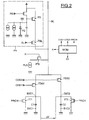
- sampling capacitors C1, C2 is connected to each column of the matrix via sampling transistors as shown in Figure 2.
- MLCT reading means of conventional structure are known per se and allow a reading of the charges stored in the sampling capacitor C1, C2.
- Such reading means can present an architecture allowing a reading in tension of the pixel signal, or an architecture allowing physical transfer charges contained in the sampling capacitors in two feedback capacitors connected between the inputs and the outputs of a differential sense amplifier.
- Such architecture is for example described in the French patent application n ° 0300360 at name of the Applicant.
- Reading media can also conventionally comprise an analog-digital converter by column.
- each pixel PX comprises a photodiode PD whose cathode is connected to a capacitor (essentially consisting of the capacity specific of the diode, i.e. the capacity of the PN junction of the diode) as well as the supply voltage via a transistor controlled by an RS reset signal.
- the cathode of the photodiode PD is also connected to the gate of a follower transistor TS connected to a bit line (column) BL via a TSL line selection transistor.
- This transistor TSL is controlled by a signal for selecting SL lines.
- the polarization of the follower transistor TS is ensured by means polarization signal PLS connected on the bit line BL.
- the PLS polarization means here include a source of current and this is connected on the bit line BL by through an ITS switch, formed for example of a transistor MOS, controlled by a signal K.
- the two terminals B1C1 and B1C2 of the two capacitors C1 and C2 are connected to ground.
- the other terminal B2C1 of the capacitor C1 is connected to the pixel PX via a TDS1 transistor controlled on its gate by a control signal CDS1.
- the other terminal B2C2 of the capacitor C2 is connected to the pixel PX via a TDS2 transistor controlled on its gate by a control signal CDS2.
- terminals B2C1 and B2C2 of the two capacitors C1 and C2 can be connected respectively also to ground via two switches additional IT1 and IT2 both controlled by a signal, here called the preload signal, PRCH.
- All control signals are delivered by means of MCM control, made for example from voltage sources and of logic gates.
- the pixel PX is said to be "active" because it contains a device amplification formed in this example by the follower transistor TS.
- the light signal picked up by the pixel can be general modeled by a voltage generator applying to the grid of the transistor TS successively two different voltage levels Vi (initial) and Vf (final).
- the useful signal Vs (at the pixel level) corresponds then the difference between these two levels Vi and Vf.
- the TSL transistor is, when it is on, a switch conductor, which allows the source of the follower transistor TS to be connected at the bit line. At a given moment, only one pixel is connected to it, in the occurrence is the one belonging to the selected line.
- the bias current supplied by the source PLS current bias the follower transistor TS of the pixel of the selected line.
- This transistor TS is therefore biased as a follower. Consequently, the potential of its source reproduces that of its grid, to within a Vgs offset.
- the signal voltage Vs is reproduced on the bit line, to the nearest offset Vgs.
- the voltage V BL on the bit line BL is therefore equal to Vs-Vgs.
- This order CDS 1 is a pulse that remains active for, for example, a microsecond.
- the bias current IPOL delivered by the PLS current source, is only supplied during a small fraction T1 of the duration of each sampling pulse CDS1, CDS2. This IPOL current is then cut by means of the ITS switch controlled by the control signal K.
- This first duration T1 is predetermined so as to obtain a stable final charge state for the sampling capacitor concerned.
- the nominal value of the bias current IPOL is much higher than that used in conventional architectures, typically of the order of 10 to 20 times greater. This makes it possible to achieve an all the more rapid stabilization of the voltage level V BL .
- the first duration T1 is for example of the order of 100 nanoseconds with a bias current of the order of 10 microamps.
- the gate-source voltage of the follower transistor then goes from (V t + I POL K ) at the threshold voltage V t , K being a technological constant.
- V BL of the bit line BL passes, according to the value Vi or Vf of the pixel voltage, from (V i, f - V t - I POL K ) to V i, f - V t .
- the voltage variation is positive and the current required to producing this variation passes through the follower transistor. This current quickly reaches a very low value (typically less than 100 nanoamps), and the follower transistor is weakly biased inversion. In this operating zone, the noise band is very reduced and the noise spectral density has a lower amplitude, hence a considerable improvement in noise.
Landscapes
- Engineering & Computer Science (AREA)
- Multimedia (AREA)
- Signal Processing (AREA)
- Transforming Light Signals Into Electric Signals (AREA)
Abstract
Description
- l'application à ce condensateur d'échantillonnage d'une tension égale à la tension pixel correspondante diminuée de la valeur de la tension grille-source du transistor suiveur polarisée avec un courant de polarisation constant prédéterminé, pendant une première durée prédéterminée, de façon à obtenir pour ledit condensateur d'échantillonnage, un état final de charges stable,
- l'interruption du courant de polarisation,
- la fin de l'impulsion d'échantillonnage intervenant au bout d'une deuxième durée prédéterminée après ladite interruption de courant.
- à alimenter la colonne avec ledit courant de polarisation pendant une première durée prédéterminée de façon à obtenir pour ledit condensateur d'échantillonnage un état final de charge stable,
- puis à interrompre l'alimentation de ladite colonne par le courant de polarisation,
- la fin de l'impulsion d'échantillonnage intervenant au bout d'une deuxième durée prédéterminée après ladite interruption du courant.
- la figure 1 est un synoptique schématique d'un capteur d'image selon l'invention,
- la figure 2 illustre plus en détail une partie du capteur d'image de la figure 1, et,
- la figure 3 illustre un chronogramme temporel représentatif d'un mode de mise en oeuvre de l'invention.
Claims (15)
- Procédé d'échantillonnage du signal délivré par un pixel actif d'un capteur d'images, comprenant une phase de stockage du signal dans une paire de condensateurs d'échantillonnage comportant deux liaisons électriques effectives respectives successives des deux condensateurs d'échantillonnage avec le transistor suiveur du pixel au cours de deux impulsions d'échantillonnage respectives correspondant respectivement à deux niveaux de tension pixel différents successifs appliqués sur la grille du transistor suiveur, caractérisé par le fait que la phase de stockage comporte pour chaque condensateur d'échantillonnage (C1 ; C2),l'application à ce condensateur d'échantillonnage (C1 ; C2)d'une tension égale à la tension pixel correspondante diminuée de la valeur de la tension grille-source du transistor suiveur polarisé avec un courant de polarisation constant prédéterminé, pendant une première durée prédéterminée (T1) de façon à obtenir pour ledit condensateur d'échantillonnage un état final de charge stable,l'interruption du courant de polarisation (IPOL),la fin de l'impulsion d'échantillonnage intervenant au bout d'une deuxième durée prédéterminée (T2) après ladite interruption du courant.
- Procédé selon la revendication 1, caractérisé par le fait que la deuxième durée (T2) est choisie de façon à obtenir à la fin de ladite impulsion d'échantillonnage, un courant résiduel circulant dans le transistor suiveur inférieur à un seuil prédéterminé correspondant à un niveau de seuil prédéterminé du bruit du transistor suiveur.
- Procédé selon la revendication 2, caractérisé par le fait que le niveau de seuil prédéterminé pour le bruit du transistor suiveur est compris entre 50 et 100 microvolts environ.
- Procédé selon l'une des revendications précédentes, caractérisé par le fait que ladite première durée (T1) est une fraction de la durée de ladite impulsion d'échantillonnage, le courant de polarisation étant alors supérieur à un seuil prédéterminé.
- Procédé selon la revendication 4, caractérisé par le fait que la durée de l'impulsion d'échantillonnage est de l'ordre de 1 microseconde, par le fait que la première durée est de l'ordre de 100 nanosecondes, et par le fait que le courant de polarisation est de l'ordre 10 microampères.
- Procédé selon l'une des revendications précédentes, caractérisé par le fait qu'on précharge (PRCH) chaque condensateur d'échantillonnage à une valeur initiale prédéterminée avant chaque impulsion d'échantillonnage.
- Capteur d'image, comprenant une matrice de pixels actifs, et des moyens de traitement des informations délivrées par ladite matrice de pixels actifs, les moyens de traitement comportant une paire de condensateurs d'échantillonnage (C1; C2) par colonne de la matrice aptes à être respectivement reliés électriquement au transistor suiveur de chaque pixel de la colonne au cours de deux impulsions d'échantillonnage respectives correspondant respectivement à deux niveaux de tension pixel différents successifs appliqués sur la grille du transistor suiveur, caractérisé par le fait que les moyens de traitement comportent une source de courant (PLS) connectée à chaque colonne de la matrice, et apte à délivrer sur commande (K) à ladite colonne un courant de polarisation constant prédéterminé, et des moyens de commande aptes pour chaque condensateur d'échantillonnage et au cours de l'impulsion d'échantillonnage correspondante,à alimenter la colonne avec ledit courant de polarisation (IPOL) pendant une première durée prédéterminée de façon à obtenir pour ledit condensateur d'échantillonnage un état final de charge stable,puis à interrompre l'alimentation de ladite colonne par le courant de polarisation,la fin de l'impulsion d'échantillonnage intervenant au bout d'une deuxième durée (T2) prédéterminée après ladite interruption du courant.
- Capteur selon la revendication 7, caractérisé par le fait que la deuxième durée est choisie de façon à obtenir à la fin de l'impulsion d'échantillonnage, un courant résiduel circulant dans le transistor suiveur inférieur à un seuil prédéterminé correspondant à un niveau de seuil prédéterminé du bruit du transistor suiveur.
- Capteur selon la revendication 8, caractérisé par le fait que le niveau de seuil prédéterminé pour le bruit du transistor suiveur est compris entre 50 et 100 microvolts environ.
- Capteur selon l'une des revendications 7 à 9, caractérisé par le fait que ladite première durée (T1) est une fraction de la durée de ladite impulsion d'échantillonnage, le courant de polarisation étant alors supérieur à un seuil prédéterminé.
- Capteur selon la revendication 10, caractérisé par le fait que la durée de l'impulsion d'échantillonnage est de l'ordre de 1 microseconde, par le fait que la première durée est de l'ordre de 100 nanosecondes, et par le fait que le courant de polarisation est de l'ordre 10 microampères.
- Capteur selon l'une des revendications 7 à 11, caractérisé par le fait que la source de courant est connectée à ladite colonne par un interrupteur commandable par les moyens de commande.
- Capteur selon l'une des revendications 7 à 12, caractérisé par le fait que les moyens de traitement comportent des moyens de précharge aptes à précharger chaque condensateur d'échantillonnage à une valeur initiale prédéterminée avant chaque impulsion d'échantillonnage.
- Capteur selon la revendication 13, caractérisé par le fait que chaque condensateur d'échantillonnage possède une borne reliée à la masse, et par le fait que les moyens de précharge comportent deux interrupteurs supplémentaires commandables (IT1 ; IT2) aptes à relier respectivement les deux autres bornes des deux condensateurs d'échantillonnage à la masse.
- Dispositif d'acquisition d'images, par exemple une caméra vidéo, caractérisé par le fait qu'il comporte au moins un capteur d'image selon l'une des revendications 7 à 14.
Applications Claiming Priority (2)
| Application Number | Priority Date | Filing Date | Title |
|---|---|---|---|
| FR0305363 | 2003-04-30 | ||
| FR0305363A FR2854529A1 (fr) | 2003-04-30 | 2003-04-30 | Procede d'echantillonnage du signal delivre par un pixel actif d'un capteur d'image, et capteur correspondant |
Publications (2)
| Publication Number | Publication Date |
|---|---|
| EP1473927A1 true EP1473927A1 (fr) | 2004-11-03 |
| EP1473927B1 EP1473927B1 (fr) | 2005-12-07 |
Family
ID=32982347
Family Applications (1)
| Application Number | Title | Priority Date | Filing Date |
|---|---|---|---|
| EP04290772A Expired - Lifetime EP1473927B1 (fr) | 2003-04-30 | 2004-03-23 | Procédé d'échantillonnage du signal délivré par un pixel actif d'un capteur d'image, et capteur correspondant |
Country Status (4)
| Country | Link |
|---|---|
| US (1) | US20040263656A1 (fr) |
| EP (1) | EP1473927B1 (fr) |
| DE (1) | DE602004000219D1 (fr) |
| FR (1) | FR2854529A1 (fr) |
Families Citing this family (5)
| Publication number | Priority date | Publication date | Assignee | Title |
|---|---|---|---|---|
| US7969493B2 (en) * | 2006-03-20 | 2011-06-28 | Intellectual Ventures Fund 27 Llc | Matching free dynamic digital pixel sensor |
| US7368698B2 (en) * | 2006-04-12 | 2008-05-06 | Micron Technology, Inc. | Imaging device with reduced row readout time and method of operating the same |
| FR3094598A1 (fr) * | 2019-03-29 | 2020-10-02 | Stmicroelectronics (Grenoble 2) Sas | Pixel et son procédé de commande |
| FR3096856B1 (fr) | 2019-06-03 | 2021-06-25 | St Microelectronics Grenoble 2 | Capteur d'image et son procédé de commande |
| FR3096855B1 (fr) | 2019-06-03 | 2022-08-05 | St Microelectronics Grenoble 2 | Capteur d'image et son procédé de commande |
Citations (2)
| Publication number | Priority date | Publication date | Assignee | Title |
|---|---|---|---|---|
| US20010033337A1 (en) * | 2000-03-02 | 2001-10-25 | Takamasa Sakuragi | Image pickup apparatus |
| US20020175269A1 (en) * | 2001-04-04 | 2002-11-28 | Krymski Alexander I. | Method and apparatus for reducing kTC noise in an active pixel sensor (APS) device |
Family Cites Families (9)
| Publication number | Priority date | Publication date | Assignee | Title |
|---|---|---|---|---|
| US5841126A (en) * | 1994-01-28 | 1998-11-24 | California Institute Of Technology | CMOS active pixel sensor type imaging system on a chip |
| GB9619088D0 (en) * | 1996-09-12 | 1996-10-23 | Vlsi Vision Ltd | Ofset cancellation in array image sensors |
| US6606122B1 (en) * | 1997-09-29 | 2003-08-12 | California Institute Of Technology | Single chip camera active pixel sensor |
| US6421085B1 (en) * | 1998-04-14 | 2002-07-16 | Eastman Kodak Company | High speed CMOS imager column CDS circuit |
| US6128039A (en) * | 1999-01-11 | 2000-10-03 | Omnivision Technologies, Inc. | Column amplifier for high fixed pattern noise reduction |
| US6727946B1 (en) * | 1999-12-14 | 2004-04-27 | Omnivision Technologies, Inc. | APS soft reset circuit for reducing image lag |
| EP1351492B1 (fr) * | 2002-04-05 | 2006-06-14 | STMicroelectronics Limited | Améliorations dans les capteurs d'images actifs |
| US6919551B2 (en) * | 2002-08-29 | 2005-07-19 | Micron Technology Inc. | Differential column readout scheme for CMOS APS pixels |
| US7365784B2 (en) * | 2003-04-15 | 2008-04-29 | Micron Technology, Inc. | Column sample-and-hold cell for CMOS APS sensor |
-
2003
- 2003-04-30 FR FR0305363A patent/FR2854529A1/fr active Pending
-
2004
- 2004-03-23 DE DE602004000219T patent/DE602004000219D1/de not_active Expired - Lifetime
- 2004-03-23 EP EP04290772A patent/EP1473927B1/fr not_active Expired - Lifetime
- 2004-04-19 US US10/827,094 patent/US20040263656A1/en not_active Abandoned
Patent Citations (2)
| Publication number | Priority date | Publication date | Assignee | Title |
|---|---|---|---|---|
| US20010033337A1 (en) * | 2000-03-02 | 2001-10-25 | Takamasa Sakuragi | Image pickup apparatus |
| US20020175269A1 (en) * | 2001-04-04 | 2002-11-28 | Krymski Alexander I. | Method and apparatus for reducing kTC noise in an active pixel sensor (APS) device |
Also Published As
| Publication number | Publication date |
|---|---|
| US20040263656A1 (en) | 2004-12-30 |
| FR2854529A1 (fr) | 2004-11-05 |
| DE602004000219D1 (de) | 2006-01-12 |
| EP1473927B1 (fr) | 2005-12-07 |
Similar Documents
| Publication | Publication Date | Title |
|---|---|---|
| EP0237365B1 (fr) | Dispositif photosensible | |
| EP0364351B1 (fr) | Procédé de détection photoélectrique avec réduction de rémanence de photo-transistor, notamment de type NIPIN | |
| EP3140906B1 (fr) | Dispositif haute dynamique pour l'integration d'un courant electrique | |
| FR3094598A1 (fr) | Pixel et son procédé de commande | |
| FR2638286A1 (fr) | Dispositif photosensible du type a amplification du signal au niveau des points photosensibles | |
| FR2636800A1 (fr) | Procede de lecture de cellules photosensibles du type comportant deux diodes montees en serie avec des sens de conduction opposes | |
| FR3096855A1 (fr) | Capteur d'image et son procédé de commande | |
| EP3386186B1 (fr) | Capteur d'images | |
| EP0331546B1 (fr) | Matrice photosensible à deux diodes par point, sans conducteur spécifique de remise à niveau | |
| EP1473927B1 (fr) | Procédé d'échantillonnage du signal délivré par un pixel actif d'un capteur d'image, et capteur correspondant | |
| EP1256984A2 (fr) | Photod-tecteur CMOS comportant une photodiode en silicium amorphe | |
| EP3319311B1 (fr) | Capteur d'images synchrone à codage temporel | |
| FR3105576A1 (fr) | Pixel à faible bruit pour capteur d'image | |
| EP0965224B1 (fr) | Procede de commande d'un dispositif photosensible a faible remanence, et dispositif photosensible mettant en oeuvre le procede | |
| FR2962851A1 (fr) | Capteur d'image | |
| FR2866180A1 (fr) | Procede de traitement des informations delivrees par une matrice de pixels actifs d'un capteur offrant une dynamique et un gain etendus, et capteur correspondant. | |
| EP1796373A1 (fr) | Pocédé d'obtention d'une image à l'aide d'un capteur d'images à gamme dynamique etendue | |
| EP2966687A1 (fr) | Capteur d'images cmos | |
| FR2513015A1 (fr) | Dispositif de detection d'image en couleurs du type transfert de charge | |
| FR2936118A1 (fr) | Compteur analogique et imageur incorporant un tel compteur. | |
| CA2449939C (fr) | Procede de commande d'un dispositif photosensible | |
| FR2508234A1 (fr) | Ensemble detecteur photonique, lecteur a transfert de charges adapte et cible de prise de vues utilisant un tel ensemble | |
| EP4262228B1 (fr) | Matrice de pixels | |
| FR2992813A1 (fr) | Procede de commande d'un pixel cmos | |
| WO2020049460A1 (fr) | Dispositif imageur à grande vitesse d'acquisition et à gamme dynamique étendue |
Legal Events
| Date | Code | Title | Description |
|---|---|---|---|
| PUAI | Public reference made under article 153(3) epc to a published international application that has entered the european phase |
Free format text: ORIGINAL CODE: 0009012 |
|
| AK | Designated contracting states |
Kind code of ref document: A1 Designated state(s): AT BE BG CH CY CZ DE DK EE ES FI FR GB GR HU IE IT LI LU MC NL PL PT RO SE SI SK TR |
|
| AX | Request for extension of the european patent |
Extension state: AL HR LT LV MK |
|
| GRAP | Despatch of communication of intention to grant a patent |
Free format text: ORIGINAL CODE: EPIDOSNIGR1 |
|
| 17P | Request for examination filed |
Effective date: 20050428 |
|
| AKX | Designation fees paid |
Designated state(s): DE FR GB |
|
| GRAS | Grant fee paid |
Free format text: ORIGINAL CODE: EPIDOSNIGR3 |
|
| GRAA | (expected) grant |
Free format text: ORIGINAL CODE: 0009210 |
|
| AK | Designated contracting states |
Kind code of ref document: B1 Designated state(s): DE FR GB |
|
| REG | Reference to a national code |
Ref country code: GB Ref legal event code: FG4D Free format text: NOT ENGLISH |
|
| GBT | Gb: translation of ep patent filed (gb section 77(6)(a)/1977) |
Effective date: 20051207 |
|
| REF | Corresponds to: |
Ref document number: 602004000219 Country of ref document: DE Date of ref document: 20060112 Kind code of ref document: P |
|
| PG25 | Lapsed in a contracting state [announced via postgrant information from national office to epo] |
Ref country code: DE Free format text: LAPSE BECAUSE OF FAILURE TO SUBMIT A TRANSLATION OF THE DESCRIPTION OR TO PAY THE FEE WITHIN THE PRESCRIBED TIME-LIMIT Effective date: 20060308 |
|
| PLBE | No opposition filed within time limit |
Free format text: ORIGINAL CODE: 0009261 |
|
| STAA | Information on the status of an ep patent application or granted ep patent |
Free format text: STATUS: NO OPPOSITION FILED WITHIN TIME LIMIT |
|
| 26N | No opposition filed |
Effective date: 20060908 |
|
| PGFP | Annual fee paid to national office [announced via postgrant information from national office to epo] |
Ref country code: GB Payment date: 20080225 Year of fee payment: 5 |
|
| PGFP | Annual fee paid to national office [announced via postgrant information from national office to epo] |
Ref country code: FR Payment date: 20080328 Year of fee payment: 5 |
|
| GBPC | Gb: european patent ceased through non-payment of renewal fee |
Effective date: 20090323 |
|
| REG | Reference to a national code |
Ref country code: FR Ref legal event code: ST Effective date: 20091130 |
|
| PG25 | Lapsed in a contracting state [announced via postgrant information from national office to epo] |
Ref country code: GB Free format text: LAPSE BECAUSE OF NON-PAYMENT OF DUE FEES Effective date: 20090323 Ref country code: FR Free format text: LAPSE BECAUSE OF NON-PAYMENT OF DUE FEES Effective date: 20091123 |