EP1473349A2 - Organic electroluminescent devices, aminostyrylnaphthalene compounds and synthesis intermediates thereof, and production processes of the same - Google Patents
Organic electroluminescent devices, aminostyrylnaphthalene compounds and synthesis intermediates thereof, and production processes of the same Download PDFInfo
- Publication number
- EP1473349A2 EP1473349A2 EP04007087A EP04007087A EP1473349A2 EP 1473349 A2 EP1473349 A2 EP 1473349A2 EP 04007087 A EP04007087 A EP 04007087A EP 04007087 A EP04007087 A EP 04007087A EP 1473349 A2 EP1473349 A2 EP 1473349A2
- Authority
- EP
- European Patent Office
- Prior art keywords
- group
- saturated
- substituted
- unsubstituted
- unsaturated
- Prior art date
- Legal status (The legal status is an assumption and is not a legal conclusion. Google has not performed a legal analysis and makes no representation as to the accuracy of the status listed.)
- Withdrawn
Links
- 0 CC*(*)c(cc1)ccc1NC=N[C@@]1C=Cc2c(*)c(*)ccc2C1C Chemical compound CC*(*)c(cc1)ccc1NC=N[C@@]1C=Cc2c(*)c(*)ccc2C1C 0.000 description 16
Images


Classifications
-
- C—CHEMISTRY; METALLURGY
- C07—ORGANIC CHEMISTRY
- C07C—ACYCLIC OR CARBOCYCLIC COMPOUNDS
- C07C255/00—Carboxylic acid nitriles
- C07C255/49—Carboxylic acid nitriles having cyano groups bound to carbon atoms of six-membered aromatic rings of a carbon skeleton
- C07C255/58—Carboxylic acid nitriles having cyano groups bound to carbon atoms of six-membered aromatic rings of a carbon skeleton containing cyano groups and singly-bound nitrogen atoms, not being further bound to other hetero atoms, bound to the carbon skeleton
-
- C—CHEMISTRY; METALLURGY
- C07—ORGANIC CHEMISTRY
- C07C—ACYCLIC OR CARBOCYCLIC COMPOUNDS
- C07C255/00—Carboxylic acid nitriles
- C07C255/49—Carboxylic acid nitriles having cyano groups bound to carbon atoms of six-membered aromatic rings of a carbon skeleton
- C07C255/58—Carboxylic acid nitriles having cyano groups bound to carbon atoms of six-membered aromatic rings of a carbon skeleton containing cyano groups and singly-bound nitrogen atoms, not being further bound to other hetero atoms, bound to the carbon skeleton
- C07C255/59—Carboxylic acid nitriles having cyano groups bound to carbon atoms of six-membered aromatic rings of a carbon skeleton containing cyano groups and singly-bound nitrogen atoms, not being further bound to other hetero atoms, bound to the carbon skeleton the carbon skeleton being further substituted by singly-bound oxygen atoms
-
- C—CHEMISTRY; METALLURGY
- C07—ORGANIC CHEMISTRY
- C07F—ACYCLIC, CARBOCYCLIC OR HETEROCYCLIC COMPOUNDS CONTAINING ELEMENTS OTHER THAN CARBON, HYDROGEN, HALOGEN, OXYGEN, NITROGEN, SULFUR, SELENIUM OR TELLURIUM
- C07F9/00—Compounds containing elements of Groups 5 or 15 of the Periodic Table
- C07F9/02—Phosphorus compounds
- C07F9/28—Phosphorus compounds with one or more P—C bonds
- C07F9/38—Phosphonic acids [RP(=O)(OH)2]; Thiophosphonic acids ; [RP(=X1)(X2H)2(X1, X2 are each independently O, S or Se)]
- C07F9/40—Esters thereof
- C07F9/4003—Esters thereof the acid moiety containing a substituent or a structure which is considered as characteristic
- C07F9/4056—Esters of arylalkanephosphonic acids
-
- C—CHEMISTRY; METALLURGY
- C07—ORGANIC CHEMISTRY
- C07F—ACYCLIC, CARBOCYCLIC OR HETEROCYCLIC COMPOUNDS CONTAINING ELEMENTS OTHER THAN CARBON, HYDROGEN, HALOGEN, OXYGEN, NITROGEN, SULFUR, SELENIUM OR TELLURIUM
- C07F9/00—Compounds containing elements of Groups 5 or 15 of the Periodic Table
- C07F9/02—Phosphorus compounds
- C07F9/28—Phosphorus compounds with one or more P—C bonds
- C07F9/54—Quaternary phosphonium compounds
- C07F9/5456—Arylalkanephosphonium compounds
-
- C—CHEMISTRY; METALLURGY
- C09—DYES; PAINTS; POLISHES; NATURAL RESINS; ADHESIVES; COMPOSITIONS NOT OTHERWISE PROVIDED FOR; APPLICATIONS OF MATERIALS NOT OTHERWISE PROVIDED FOR
- C09K—MATERIALS FOR MISCELLANEOUS APPLICATIONS, NOT PROVIDED FOR ELSEWHERE
- C09K11/00—Luminescent materials, e.g. electroluminescent or chemiluminescent
- C09K11/06—Luminescent materials, e.g. electroluminescent or chemiluminescent containing organic luminescent materials
-
- H—ELECTRICITY
- H05—ELECTRIC TECHNIQUES NOT OTHERWISE PROVIDED FOR
- H05B—ELECTRIC HEATING; ELECTRIC LIGHT SOURCES NOT OTHERWISE PROVIDED FOR; CIRCUIT ARRANGEMENTS FOR ELECTRIC LIGHT SOURCES, IN GENERAL
- H05B33/00—Electroluminescent light sources
- H05B33/12—Light sources with substantially two-dimensional [2D] radiating surfaces
- H05B33/14—Light sources with substantially two-dimensional [2D] radiating surfaces characterised by the chemical or physical composition or the arrangement of the electroluminescent material, or by the simultaneous addition of the electroluminescent material in or onto the light source
-
- H—ELECTRICITY
- H10—SEMICONDUCTOR DEVICES; ELECTRIC SOLID-STATE DEVICES NOT OTHERWISE PROVIDED FOR
- H10K—ORGANIC ELECTRIC SOLID-STATE DEVICES
- H10K85/00—Organic materials used in the body or electrodes of devices covered by this subclass
- H10K85/60—Organic compounds having low molecular weight
- H10K85/615—Polycyclic condensed aromatic hydrocarbons, e.g. anthracene
-
- H—ELECTRICITY
- H10—SEMICONDUCTOR DEVICES; ELECTRIC SOLID-STATE DEVICES NOT OTHERWISE PROVIDED FOR
- H10K—ORGANIC ELECTRIC SOLID-STATE DEVICES
- H10K85/00—Organic materials used in the body or electrodes of devices covered by this subclass
- H10K85/60—Organic compounds having low molecular weight
- H10K85/631—Amine compounds having at least two aryl rest on at least one amine-nitrogen atom, e.g. triphenylamine
-
- H—ELECTRICITY
- H10—SEMICONDUCTOR DEVICES; ELECTRIC SOLID-STATE DEVICES NOT OTHERWISE PROVIDED FOR
- H10K—ORGANIC ELECTRIC SOLID-STATE DEVICES
- H10K85/00—Organic materials used in the body or electrodes of devices covered by this subclass
- H10K85/60—Organic compounds having low molecular weight
- H10K85/631—Amine compounds having at least two aryl rest on at least one amine-nitrogen atom, e.g. triphenylamine
- H10K85/633—Amine compounds having at least two aryl rest on at least one amine-nitrogen atom, e.g. triphenylamine comprising polycyclic condensed aromatic hydrocarbons as substituents on the nitrogen atom
-
- C—CHEMISTRY; METALLURGY
- C09—DYES; PAINTS; POLISHES; NATURAL RESINS; ADHESIVES; COMPOSITIONS NOT OTHERWISE PROVIDED FOR; APPLICATIONS OF MATERIALS NOT OTHERWISE PROVIDED FOR
- C09K—MATERIALS FOR MISCELLANEOUS APPLICATIONS, NOT PROVIDED FOR ELSEWHERE
- C09K2211/00—Chemical nature of organic luminescent or tenebrescent compounds
- C09K2211/10—Non-macromolecular compounds
- C09K2211/1003—Carbocyclic compounds
- C09K2211/1011—Condensed systems
-
- C—CHEMISTRY; METALLURGY
- C09—DYES; PAINTS; POLISHES; NATURAL RESINS; ADHESIVES; COMPOSITIONS NOT OTHERWISE PROVIDED FOR; APPLICATIONS OF MATERIALS NOT OTHERWISE PROVIDED FOR
- C09K—MATERIALS FOR MISCELLANEOUS APPLICATIONS, NOT PROVIDED FOR ELSEWHERE
- C09K2211/00—Chemical nature of organic luminescent or tenebrescent compounds
- C09K2211/10—Non-macromolecular compounds
- C09K2211/1003—Carbocyclic compounds
- C09K2211/1014—Carbocyclic compounds bridged by heteroatoms, e.g. N, P, Si or B
-
- H—ELECTRICITY
- H10—SEMICONDUCTOR DEVICES; ELECTRIC SOLID-STATE DEVICES NOT OTHERWISE PROVIDED FOR
- H10K—ORGANIC ELECTRIC SOLID-STATE DEVICES
- H10K2102/00—Constructional details relating to the organic devices covered by this subclass
- H10K2102/10—Transparent electrodes, e.g. using graphene
- H10K2102/101—Transparent electrodes, e.g. using graphene comprising transparent conductive oxides [TCO]
- H10K2102/103—Transparent electrodes, e.g. using graphene comprising transparent conductive oxides [TCO] comprising indium oxides, e.g. ITO
-
- H—ELECTRICITY
- H10—SEMICONDUCTOR DEVICES; ELECTRIC SOLID-STATE DEVICES NOT OTHERWISE PROVIDED FOR
- H10K—ORGANIC ELECTRIC SOLID-STATE DEVICES
- H10K50/00—Organic light-emitting devices
- H10K50/10—OLEDs or polymer light-emitting diodes [PLED]
- H10K50/11—OLEDs or polymer light-emitting diodes [PLED] characterised by the electroluminescent [EL] layers
-
- H—ELECTRICITY
- H10—SEMICONDUCTOR DEVICES; ELECTRIC SOLID-STATE DEVICES NOT OTHERWISE PROVIDED FOR
- H10K—ORGANIC ELECTRIC SOLID-STATE DEVICES
- H10K50/00—Organic light-emitting devices
- H10K50/10—OLEDs or polymer light-emitting diodes [PLED]
- H10K50/14—Carrier transporting layers
-
- H—ELECTRICITY
- H10—SEMICONDUCTOR DEVICES; ELECTRIC SOLID-STATE DEVICES NOT OTHERWISE PROVIDED FOR
- H10K—ORGANIC ELECTRIC SOLID-STATE DEVICES
- H10K85/00—Organic materials used in the body or electrodes of devices covered by this subclass
- H10K85/30—Coordination compounds
- H10K85/321—Metal complexes comprising a group IIIA element, e.g. Tris (8-hydroxyquinoline) gallium [Gaq3]
- H10K85/324—Metal complexes comprising a group IIIA element, e.g. Tris (8-hydroxyquinoline) gallium [Gaq3] comprising aluminium, e.g. Alq3
-
- Y—GENERAL TAGGING OF NEW TECHNOLOGICAL DEVELOPMENTS; GENERAL TAGGING OF CROSS-SECTIONAL TECHNOLOGIES SPANNING OVER SEVERAL SECTIONS OF THE IPC; TECHNICAL SUBJECTS COVERED BY FORMER USPC CROSS-REFERENCE ART COLLECTIONS [XRACs] AND DIGESTS
- Y10—TECHNICAL SUBJECTS COVERED BY FORMER USPC
- Y10S—TECHNICAL SUBJECTS COVERED BY FORMER USPC CROSS-REFERENCE ART COLLECTIONS [XRACs] AND DIGESTS
- Y10S428/00—Stock material or miscellaneous articles
- Y10S428/917—Electroluminescent
Definitions
- This invention relates to organic electroluminescent devices, especially organic electroluminescent devices containing aminostyrylnaphthalene compounds useful as electron transport materials, hole transport materials or light emitting materials, the aminostyrylnaphthalene compounds useful in the organic electroluminescent devices and their synthesis intermediates, and production processes of these compounds and intermediates.
- organic electroluminescent devices are attracting attention as a candidate for flat panel displays which can produce natural light, have a high response speed and have no visibility angle dependency, and accordingly, there is an increasing interest on organic materials as their constituents.
- organic materials there are not many materials capable of forming stable red-light emitting layers in particular. Finding of such materials has, therefore, become an indispensable requirement for the realization of full-color, organic electroluminescent devices.
- aminostyryl compounds are disclosed, for example, in Japanese Patent Laid-open No.: Hei 5-105645, 2001-051433, 2002-131943, 2002-116560, 2002-099103, 2002-072511, 2002-040677, 2002-040676, 2002-031901, 2001-337469, 2001-337649, and 2000-214610.
- these compounds contain no electron attracting group in their molecules and hence, cannot be used for such applications as red-color emitting materials for organic electroluminescent devices.
- materials for organic electroluminescent devices certain compounds are disclosed in Japanese Patent Laid-open No. Hei 3-200889, Hei 5-194943, and 2002-226722.
- materials employed in white-light organic electroluminescent devices other materials are disclosed in Japanese Patent Laid-open No. Hei 6-207170. These materials are, however, not for the emission of red light either.
- materials with one or more styryl groups contained in combination with one or more triphenylamino groups are proposed in Japanese Patent Laid-open No.: Hei 5-320632, Hei 6-100857, Hei 9-268284, Hei 11-040359, Hei 11-102784, and Hei 10-245549. These materials, however, cannot be used for the emission of red light either.
- Aminostyryl compounds useful as red-light emitting materials in organic electroluminescent devices are led by the aminostyryl compounds disclosed in Inorganic and Organic Electroluminescence '96 Berlin, p.101, 1996; Journal of the Korean Chemical Society (1999), 43(3), 315-320; Bulletin of the Korean Chemical Society (2001), 22(2), 228-230; and Journal of the Korean Chemical Society (1999), 43(3), 315-320, and include those disclosed in Japanese Patent Laid-open No.: 2000-230132, 2002-022672, 2001-2883772, 2001-106657, and 2001-106658.
- asymmetrical structures may be effective in certain instances as disclosed in Japanese Patent Laid-open NO.: 2002-226722, 2001-288377, 2001-110570 (especially, page 4, right column, line 40 to page 5, right column, line 4 from the bottom; page 7, right column, line 30 to page 8, left column, line 17; FIG. 1 to FIG. 8), 2001-110571 and 2000-173773.
- Japanese Patent Laid-open No. 2002-208488 discloses that such asymmetrical structures are also effective as structural units for polymers. Further, their applications as multiphoton absorbers are also considered to be promising as disclosed in Science (1998), 281(11), 1653; WO 2001-096409; NATO Science Series, 3: High Technology (2000), 79 (Multiphoton and Light Driven Multielectron Processes in Organics), 53-65; Journal of Chemical Physics (2000), 113(10), 3951-3959; Journal of Physical Chemistry A (2001), 105(51), 11488-11495; Polymer Preprints (American Chemical Society, Division of Polymer Chemistry) (1998), 39(2), 1116; and Materials Research Society Symposium Proceedings (1998), 488 (Electrical, Optical, and Magnetic Properties of Organic Solid-State Materials IV), 217-226.
- Red-light emitting devices It is difficult to develop stable, high-luminance red-light emitting devices. Examples of those reported to date include a red-light emitting device making use of tris(8-hydroxyquinoline)aluminum (hereinafter abbreviated as "Alq 3 ”) doped with 4-dicyanomethylene-6-(p-dimethylaminostyryl)-2-methyl-4H-pyran (hereinafter abbreviated as "DCM”) (Chem. Funct. Dyes, Proc. Int. Symp., 2 nd , p.536, 1993).
- Alq 3 tris(8-hydroxyquinoline)aluminum
- DCM 4-dicyanomethylene-6-(p-dimethylaminostyryl)-2-methyl-4H-pyran
- DCJTB 4-dicyanomethylene-6-(p-dimethylaminostyryl)-2-(t-butyl)-4H-pyran
- Objects of the present invention are to provide an organic electroluminescent device capable of producing stable and high-luminance emission of red light at an optimal wavelength by using a compound improved in fluorescent wavelength over an aminostyrylnaphthalene compound which can produce emission of red light at a high fluorescence quantum yield, an aninostyrylnaphthalene compound useful in the organic electroluminescent device and its synthesis intermediates, and production processes of these compound and intermediates.
- the present invention relates to an organic electroluminescent device including an anode, a cathode, and an organic layer arranged between the anode and said cathode, wherein at least a part of the organic layer includes at least one aminostyrylnaphthalene compound represented by the below-described formula [A]; and also to the aminostyrylnaphthalene compound: wherein:
- the aminostyrylnaphthalene compound which is employed in the organic electroluminescent device according to the present invention and has the specific structure represented by the formula [A], owing to its specific structure, is excellent especially in the emission of red light, is equipped with electron transporting ability based on one or more electron attracting groups such as one or more cyano groups on a naphthalene group and also with hole transporting ability based on an aminostyryl group, and moreover, shows amorphous properties advantageous for film formability by vacuum deposition or the like and also durability especially for the inclusion of the substituent group R f (methyl, t-butyl or the like).
- Use of the aminostyrylnaphthalene compound therefore, can provide an organic electroluminescent device capable of producing high-luminance and stable emission of red light at an optimal wavelength.
- the above-described aminostyrylnaphthalene compound of the present invention can be effectively used as an organic light-emitting material capable of producing emission of red light of good chromaticy at a relatively-short, fluorescent wavelength.
- the substituent group R f methyl, t-butyl or the like
- it has a relatively small molecular weight and therefore, can reduce a thermal load to be applied upon vacuum evaporation or the like.
- it is superb in electrical, thermal or chemical stability, and is amorphous and can readily form a glass state. Accordingly, it permits vacuum deposition or the like.
- the organic electroluminescent device making use of the compound according to the present invention, red light the wavelength of which is relatively short is emitted. Therefore, the organic electroluminescent device is also advantageous in obtaining resonant light of improved color purity when the resonator structure disclosed in International publication No. WO 01/39554 is fabricated.
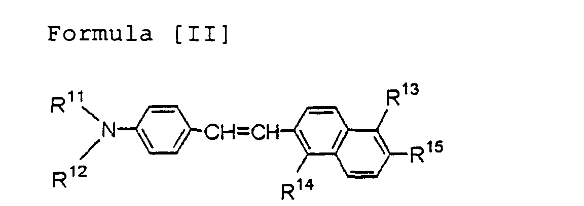
- aminostyrylnaphthalene compound of the formula [A] may preferably comprise at least one aminostyrylnaphthalene compound represented by the following formula [I], [II] or [III] : wherein:
- the aminostyrylnaphthalene compound which has the specific structure represented by the formula [I], [II] or [III], owing to its specific structure, is excellent especially in the emission of red light, is equipped with electron transporting ability based on one or more electron attracting groups such as one or more cyano groups on a naphthalene group and also with hole transporting ability based on an aminostyryl group, and moreover, shows amorphous properties advantageous for film formability by vacuum deposition or the like and also durability.
- Use of the aminostyrylnaphthalene compound therefore, can provide an organic electroluminescent device capable of producing especially high-luminance and stable emission of red light at an optimal wavelength.
- the organic layer is in a form of an organic multilayer structure comprising a hole transport layer and an electron transport layer stacked one over the other, and also that at least the electron transport layer in the organic layer comprises at least the one aminostyrylnaphthalene compound represented by the formula [A], especially the formula [I], [II] or [III].
- the organic layer is in a form of an organic multilayer structure comprising a hole transport layer and an electron transport layer stacked one over the other, and at least the hole transport layer in the organic layer comprises at least the one aminostyrylnaphthalene compound represented by the formula [A], especially the formula [I], [II] or [III].
- the organic layer is in a form of an organic multilayer structure comprising a hole transport layer, a luminescent layer and an electron transport layer stacked one over another, and at least the luminescent layer in the organic layer comprises at least the one aminostyrylnaphthalene compound represented by the formula [A], especially the formula [I], [II] or [III].
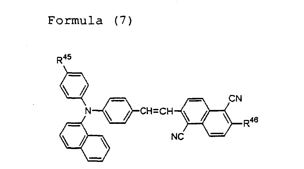
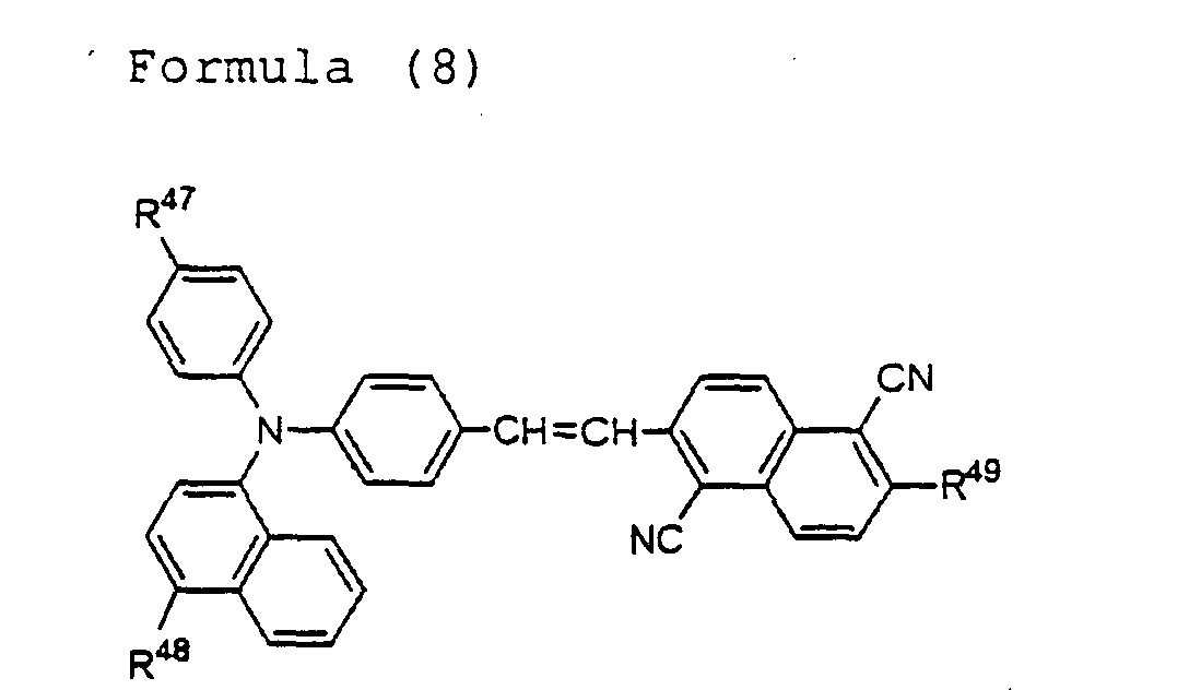
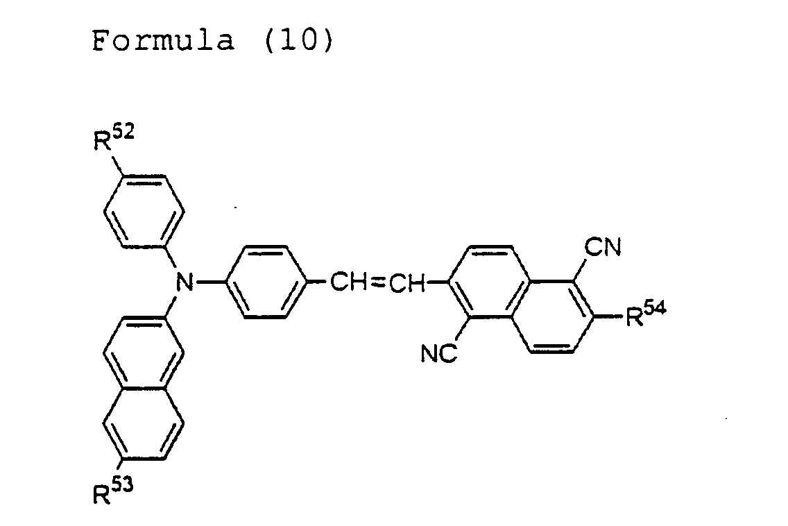
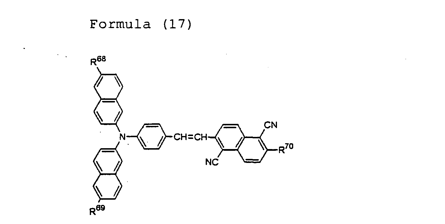
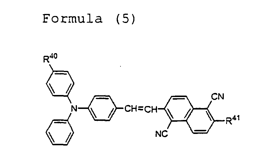
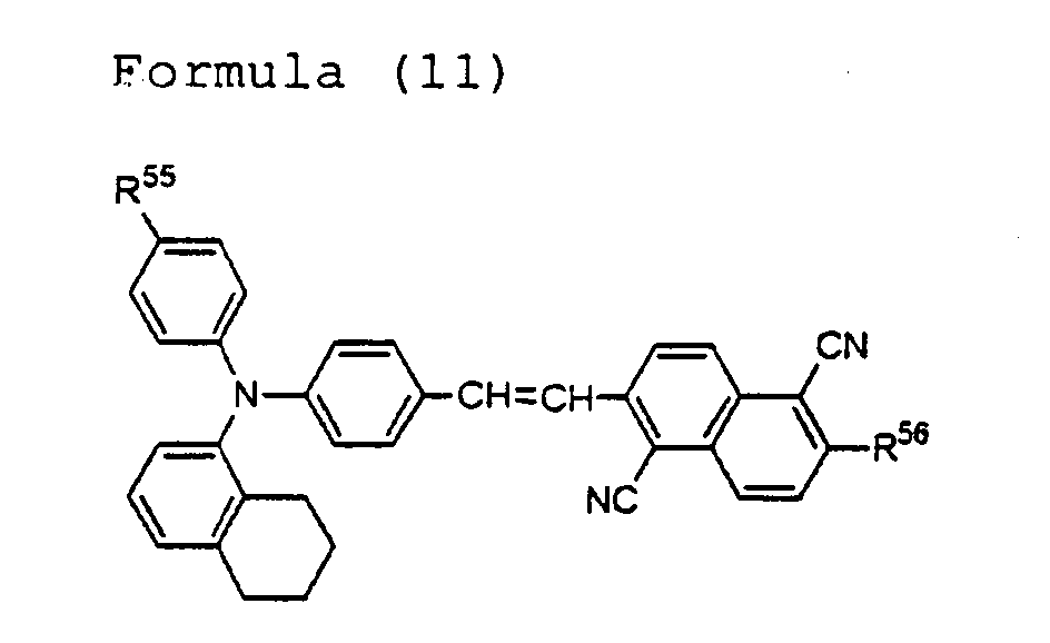
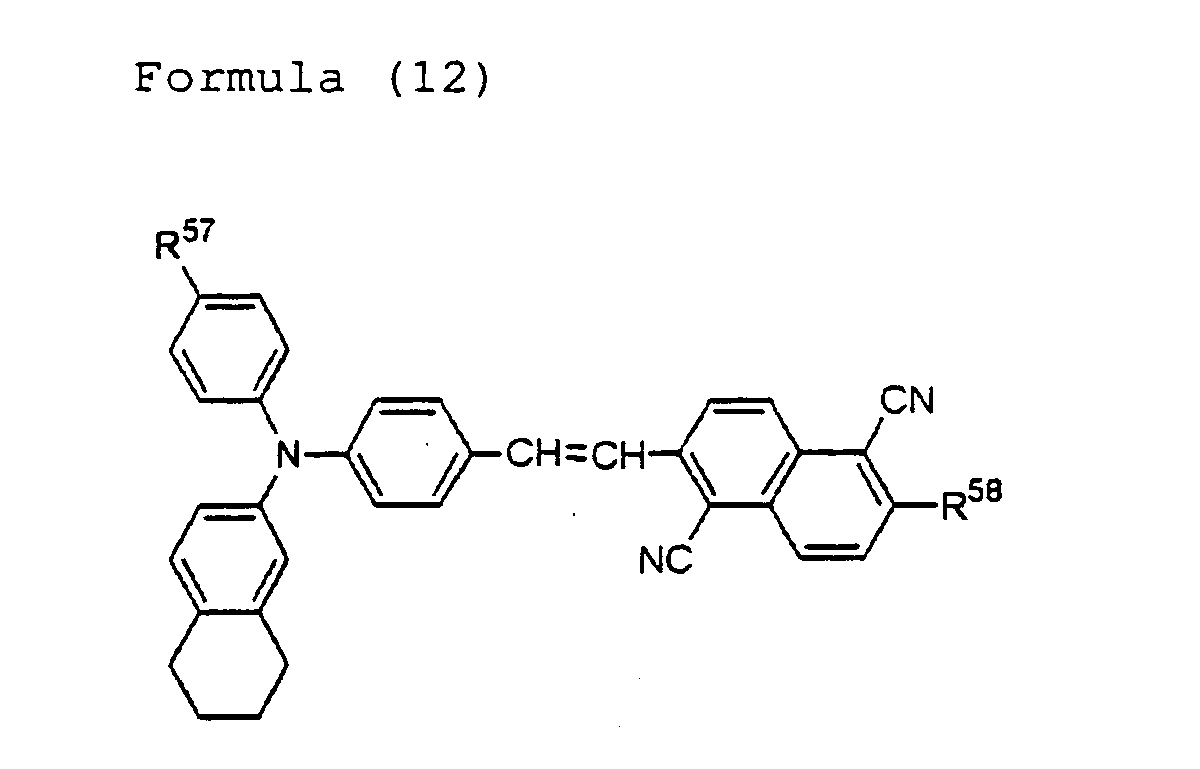
- aminostyrylnaphthalene compound may preferably be represented by the following formula (5), (6), (7), (8), (9), (10), (11), (12), (13), (14), (15), (16) or (17): wherein R 40 represents a saturated or unsaturated alkyl group having 1 to 6 carbon atoms or a substituted or unsubstituted aryl group, and R 41 has the same meaning as R 5 .
- R 42 and R 43 may be the same or different, one of R 42 and R 43 represents a saturated or unsaturated alkyl group having 1 to 6 carbon atoms or a substituted or unsubstituted aryl group, the remaining one of R 42 and R 43 represents a saturated or unsaturated alkyl group having 1 to 6 carbon atoms or a substituted or unsubstituted aryl group, and R 44 has the same meaning as R 5 .
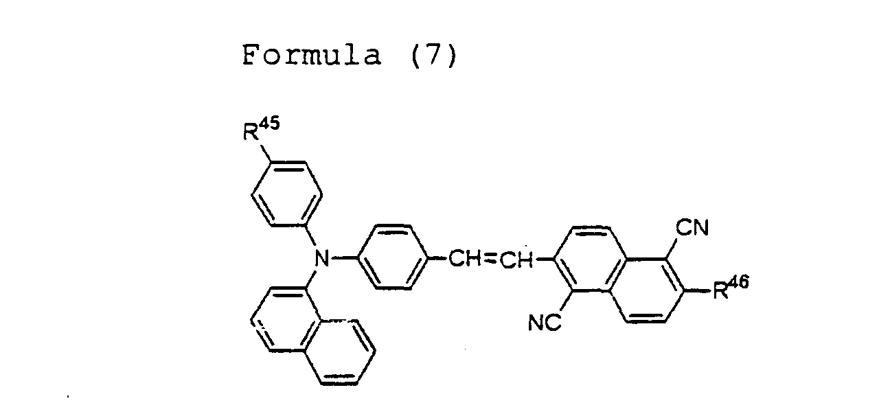
- R 45 represents a saturated or unsaturated alkyl group having 1 to 6 carbon atoms or a substituted or unsubstituted aryl group
- R 46 has the same meaning as R 27 .
- R 47 and R 48 may be the same or different and each independently represents a saturated or unsaturated alkyl group having 1 to 6 carbon atoms or a substituted or unsubstituted aryl group, and R 49 has the same meaning as R 27 .
- R 50 represents a saturated or unsaturated alkyl group having 1 to 6 carbon atoms or a substituted or unsubstituted aryl group, and R 51 has the same meaning as R 27 .
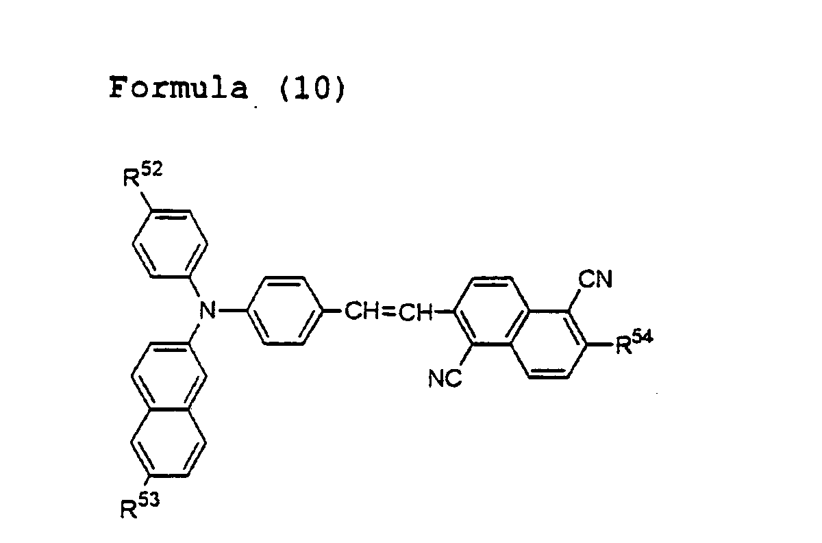
- R 52 and R 53 may be the same or different, one of R 52 and R 53 represents a saturated or unsaturated alkyl group having 1 to 6 carbon atoms or a substituted or unsubstituted aryl group, the remaining one of R 52 and R 53 represents a saturated or unsaturated alkyl group having 1 to 6 carbon atoms or a substituted or unsubstituted aryl group, and R 54 has the same meaning as R 27 .
- R 55 represents a saturated or unsaturated alkyl group having 1 to 6 carbon atoms or a substituted or unsubstituted aryl group
- R 56 has the same meaning as R 5 .
- R 57 represents a saturated or unsaturated alkyl group having 1 to 6 carbon atoms or a substituted or unsubstituted aryl group
- R 58 has the same meaning as R 5
- R 59 represents a saturated or unsaturated alkyl group having 1 to 6 carbon atoms or a substituted or unsubstituted aryl group
- R 60 has the same meaning as R 5
- R 61 represents a saturated or unsaturated alkyl group having 1 to 6 carbon atoms or a substituted or unsubstituted aryl group
- R 62 has the same meaning as R 15 .
- R 63 and R 64 may be the same or different, one of R 63 and R 64 represents a saturated or unsaturated alkyl group having 1 to 6 carbon atoms or a substituted or unsubstituted aryl group, the remaining one of R 63 and R 64 represents a saturated or unsaturated alkyl group having 1 to 6 carbon atoms or a substituted or unsubstituted aryl group, and R 65 has the same meaning as R 15 .
- R 66 represents a saturated or unsaturated alkyl group having 1 to 6 carbon atoms or a substituted or unsubstituted aryl group
- R 67 has the same meaning as R 15 .
- R 68 and R 69 may be the same or different, one of R 68 and R 69 represents a saturated or unsaturated alkyl group having 1 to 6 carbon atoms or a substituted or unsubstituted aryl group, the remaining one of R 68 and R 69 represents a saturated or unsaturated alkyl group having 1 to 6 carbon atoms or a substituted or unsubstituted aryl group, and R 70 has the same meaning as R 15 .
- the present invention also provides an aminostyrylnaphthalene compound represented by the above-described formula [A], especially the above-described formula [I], [II] or [III].
- the above-described aminostyrylnaphthalene compound of the present invention can be effectively used as an organic light-emitting material capable of producing emission of red light of good chromaticy at a relatively-short, fluorescent wavelength.
- the substituent group R f especially, R 5 , R 15 or R 27
- it has a relatively small molecular weight and therefore, can reduce a thermal load to be applied upon vacuum evaporation or the like.
- it is superb in electrical, thermal or chemical stability, and is amorphous and can readily form a glass state. Accordingly, it permits vacuum deposition or the like.
- red light the wavelength of which is relatively short can be emitted.
- the organic electroluminescent device is also advantageous in obtaining resonant light of improved color purity when the resonator structure disclosed in WO 01/39554 is fabricated.
- These advantageous features can be brought about especially when the groups R c , R d , R e , R g , R h and R i are electron-attracting groups such as cyano groups.
- these groups may all be hydrogen atoms although emission of light other than red light, for example, emission of green light is obtained in such a case.
- the compound according to the present invention may preferably be represented by any one of the above-described formulas (5) to (17).
- Examples of materials usable for the formation of the organic electroluminescent device according to the present invention can include, in addition to the compounds according to the present invention, hole transport materials (for example, aromatic amines and the like), electron transport materials (for example, Alq 3 , pyrazoline and the like), and a series of compounds commonly employed as red emission dopants (DCM and its analogous compounds, porphyrins, phthalocyanines, perylene compounds, Nile Red, squalilium compounds, and the like).
- hole transport materials for example, aromatic amines and the like
- electron transport materials for example, Alq 3 , pyrazoline and the like
- DCM red emission dopants
- DCM red emission dopants
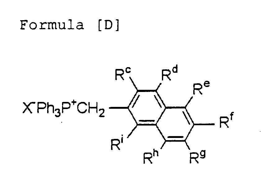
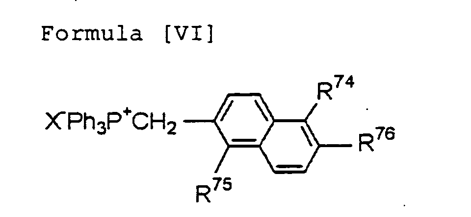
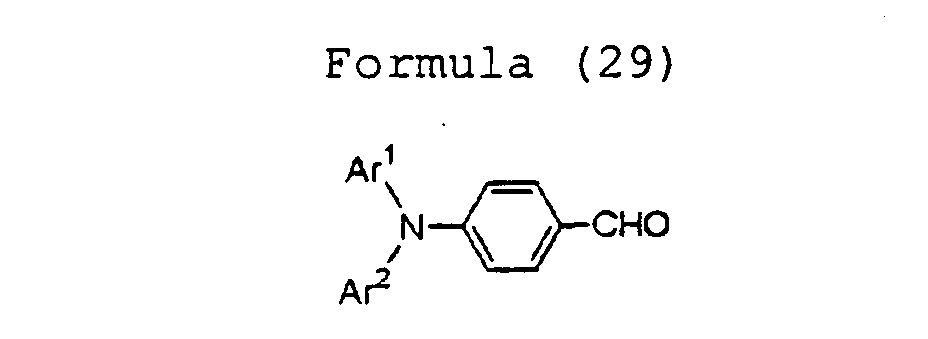
- the present invention also provides a process for the production of an aminostyrylnaphthalene compound represented by the formula [A], especially the formula [I], [II] or [III], which comprises subjecting an aminobenzaldehyde represented by the following formula [B], especially the following formula [IV] and at least one of a phosphonate ester represented by the following formula [C], especially the following formula [V] and a phosphonium represented by the following formula [D], especially the following formula [VI] to condensation: wherein R a and R b have the same meaning as defined above.
- R 71 and R 72 each independently represents an aryl group corresponding to R 1 , R 2 , R 11 , R 12 , R 23 or R 24 .
- R j represents a hydrocarbon group
- R c , R d , R e , R f , R g , R h or R i have the same meanings as defined above
- X represents a halogen atom.
- R 73 represents a hydrocarbon group, preferably a saturated hydrocarbon group having 1 to 4 carbon atoms
- R 74 and R 75 each independently represents a group corresponding to R 3 , R 4 , R 13 , R 14 , R 25 or R 26
- R 76 represents a group corresponding to R 5 , R 15 or R 27
- X represents a halogen atom.
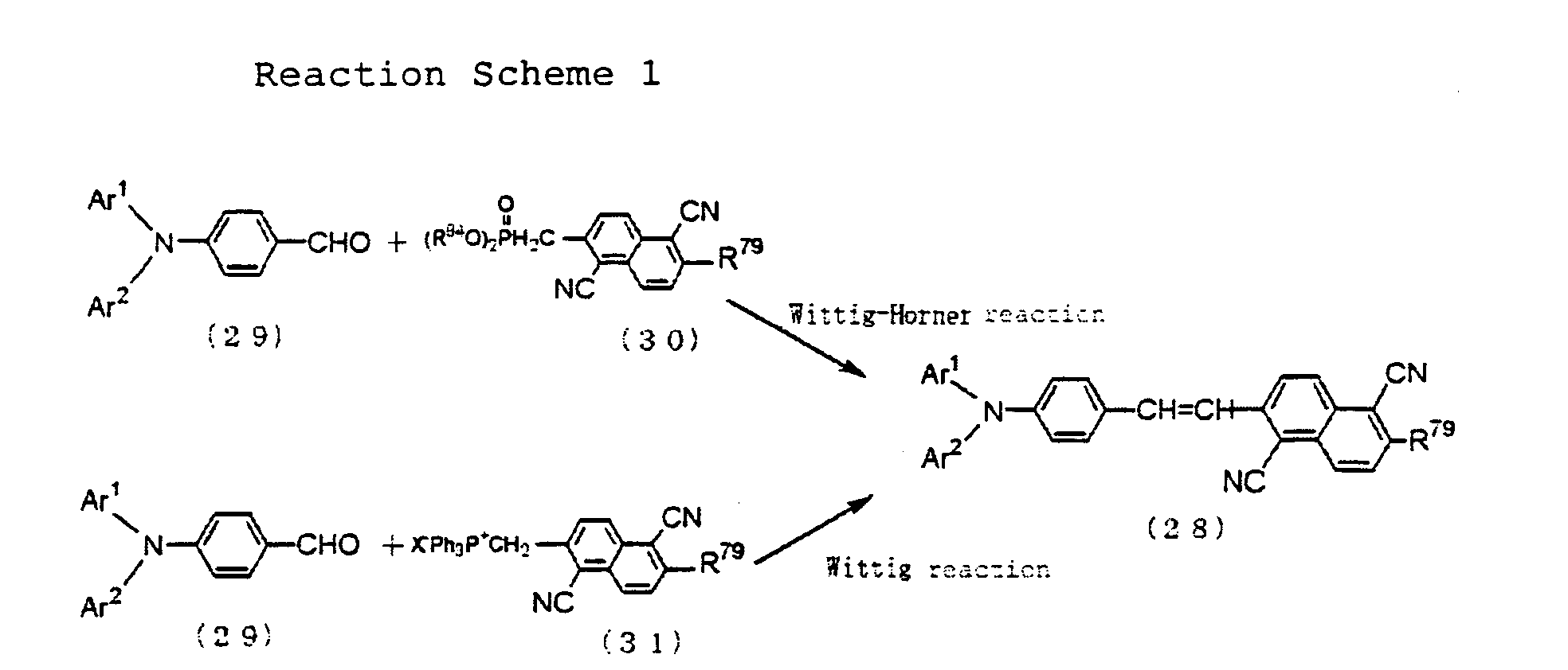
- the condensation may be conducted by the Wittig-Horner reaction or the Wittig reaction, at least one of the phosphonate ester and the phosphonium may be treated with a base in a solvent to form carbanions, and the carbanions and the aminobenzaldehyde, especially the 4-(N,N-diarylamino)benzaldehyde may be subjected to condensation.
- Ar 1 , Ar 2 , R 79 and X have the same meanings as defined above.
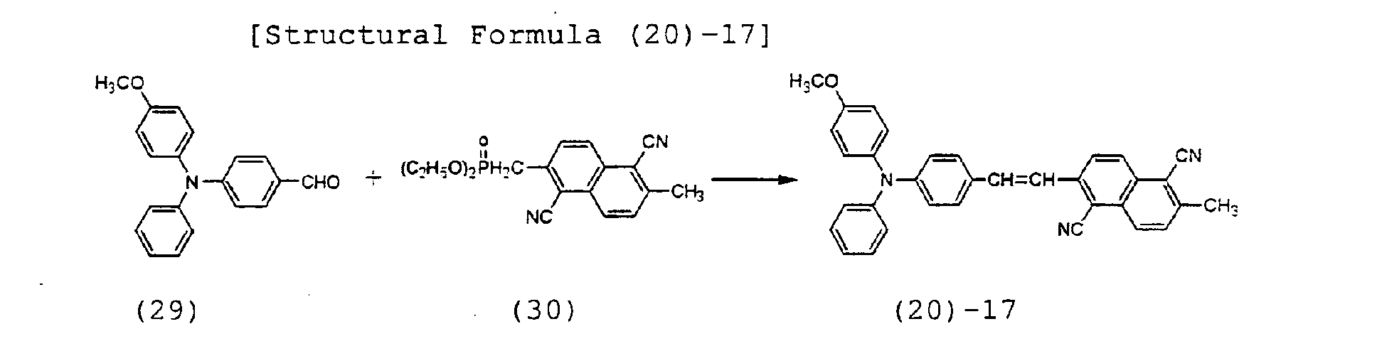
- the reactions firstly begin with the treatment of at least one of the compound of the formula (30) and the compound of the formula (31) with a base in an adequate solvent to produce carbanions. These carbanions and the aldehyde of the formula (29) are then subjected to condensation such that the reactions are completed.
- the combination of the base and the solvent the following combinations can be mentioned.
- the target product can be readily purified by chromatography, and owing to the high crystallinity of the compound of the present invention represented by the formula (28), its purity can be increased further by recrystallization.
- recrystallization may be conveniently conducted by dissolving the compound in acetone and then adding hexane to the resulting solution or by dissolving the compound in toluene under heat, concentrating the thus-prepared solution and then cooling the resultant concentrate.
- the reactions may be brought to completion in 3 to 24 hours under normal pressure.
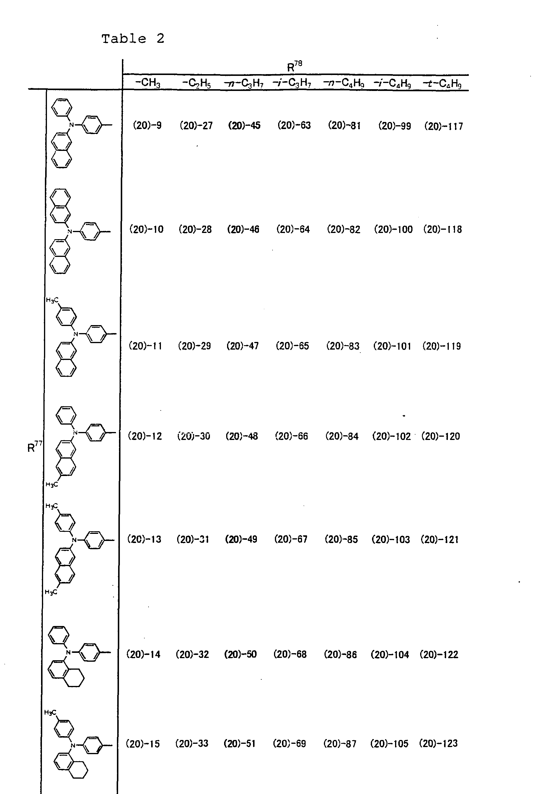
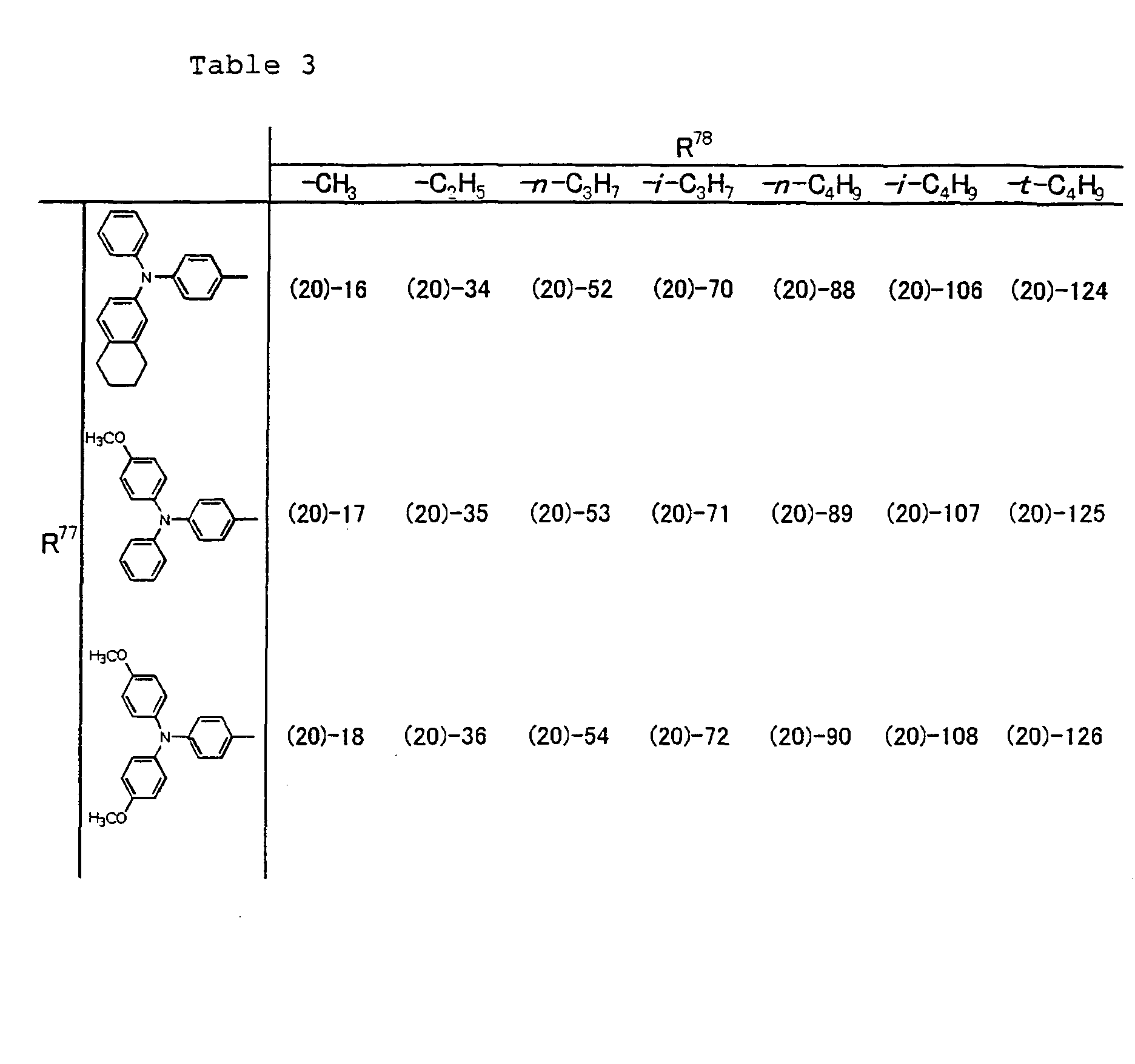
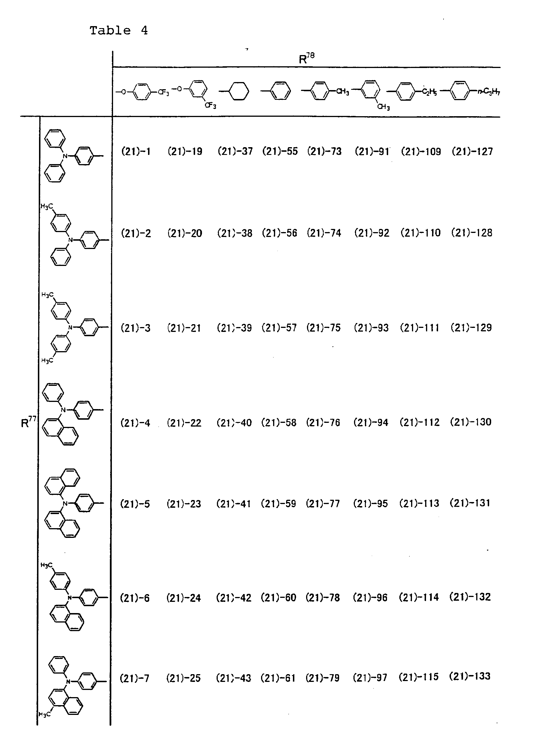
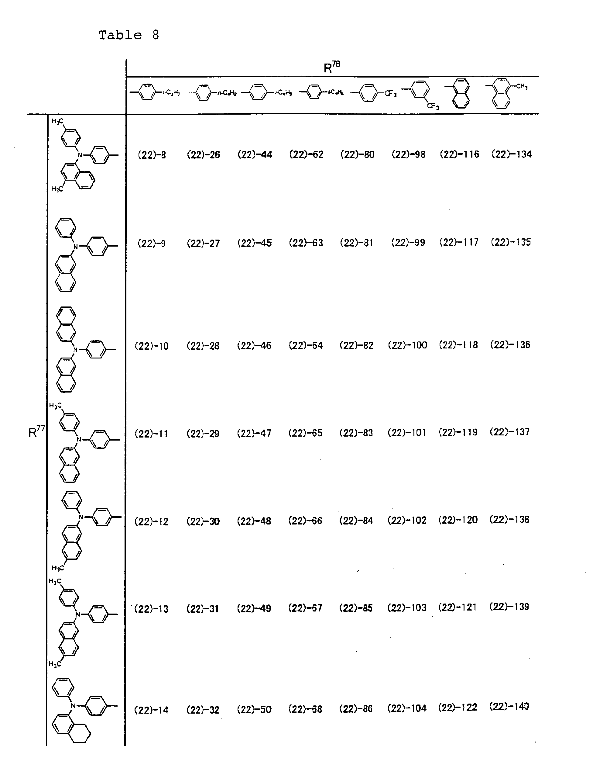
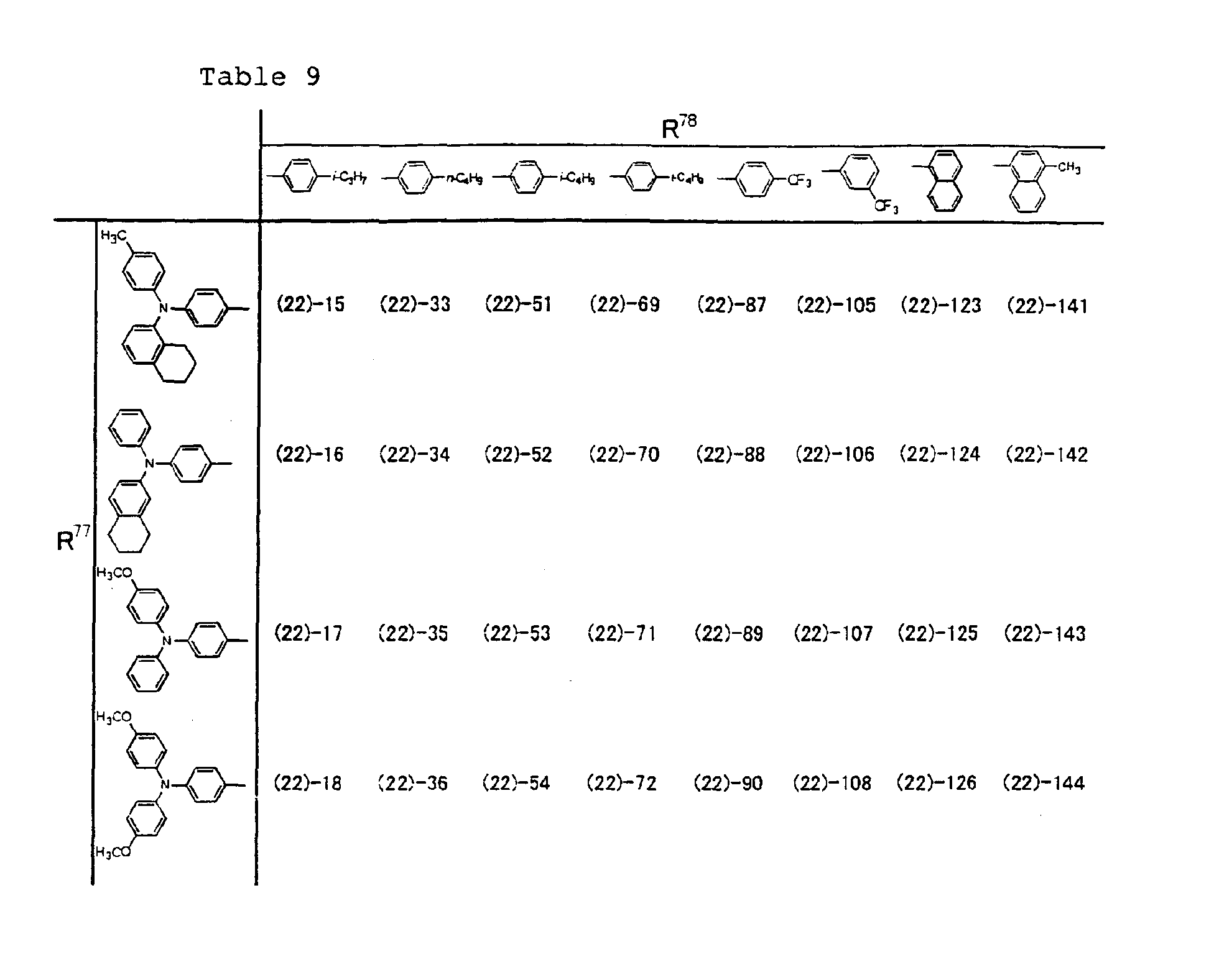
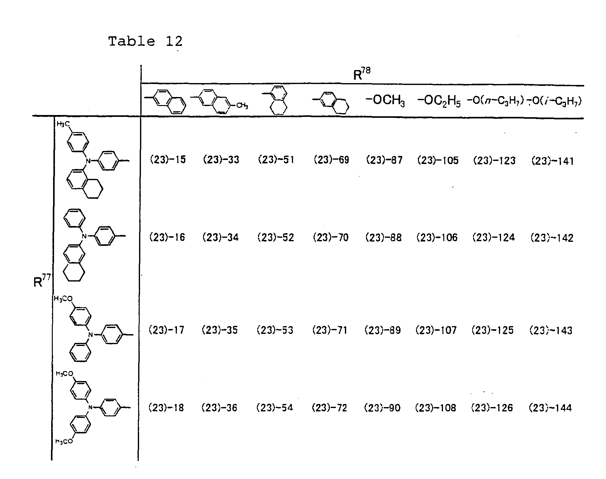
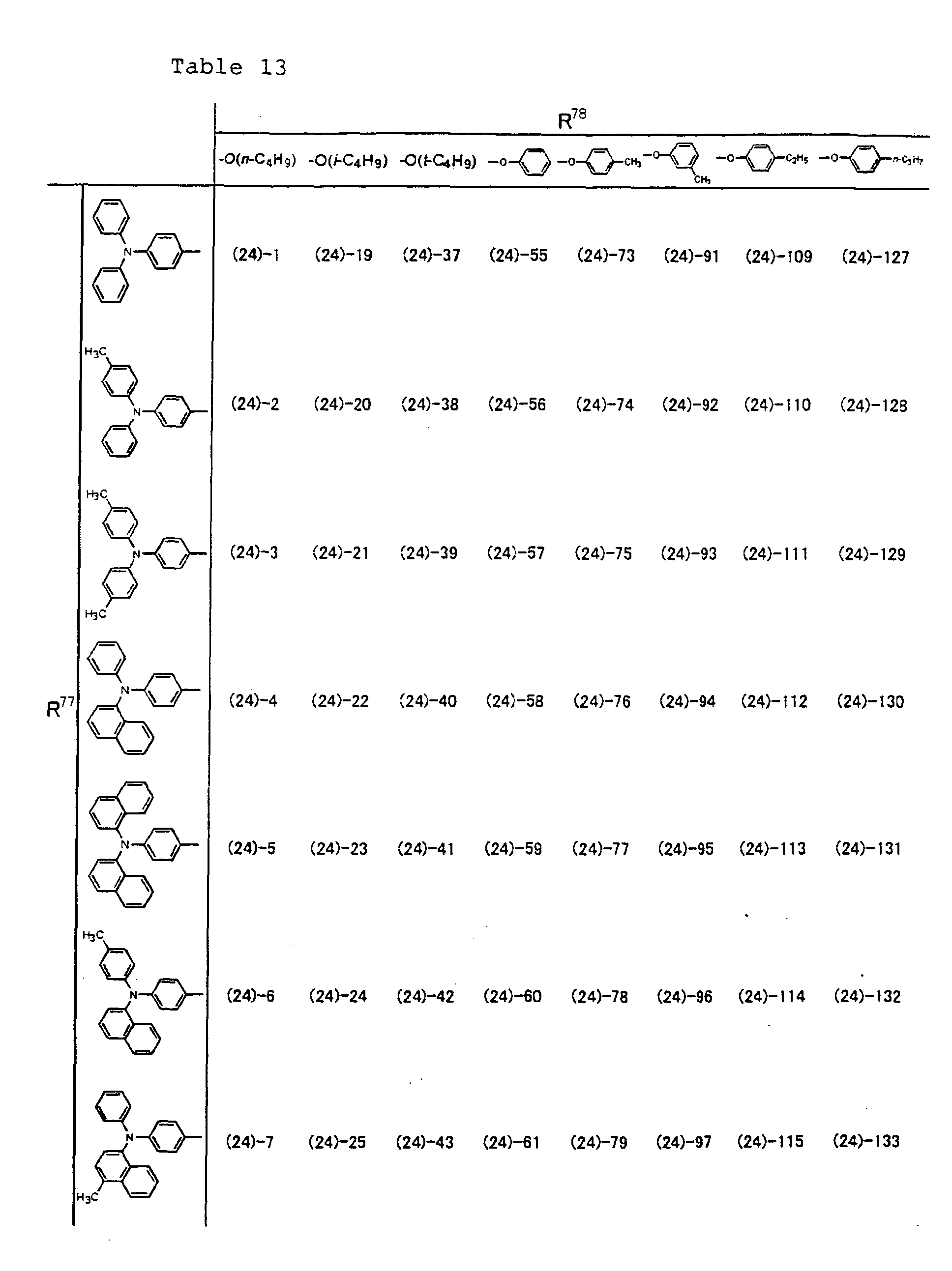
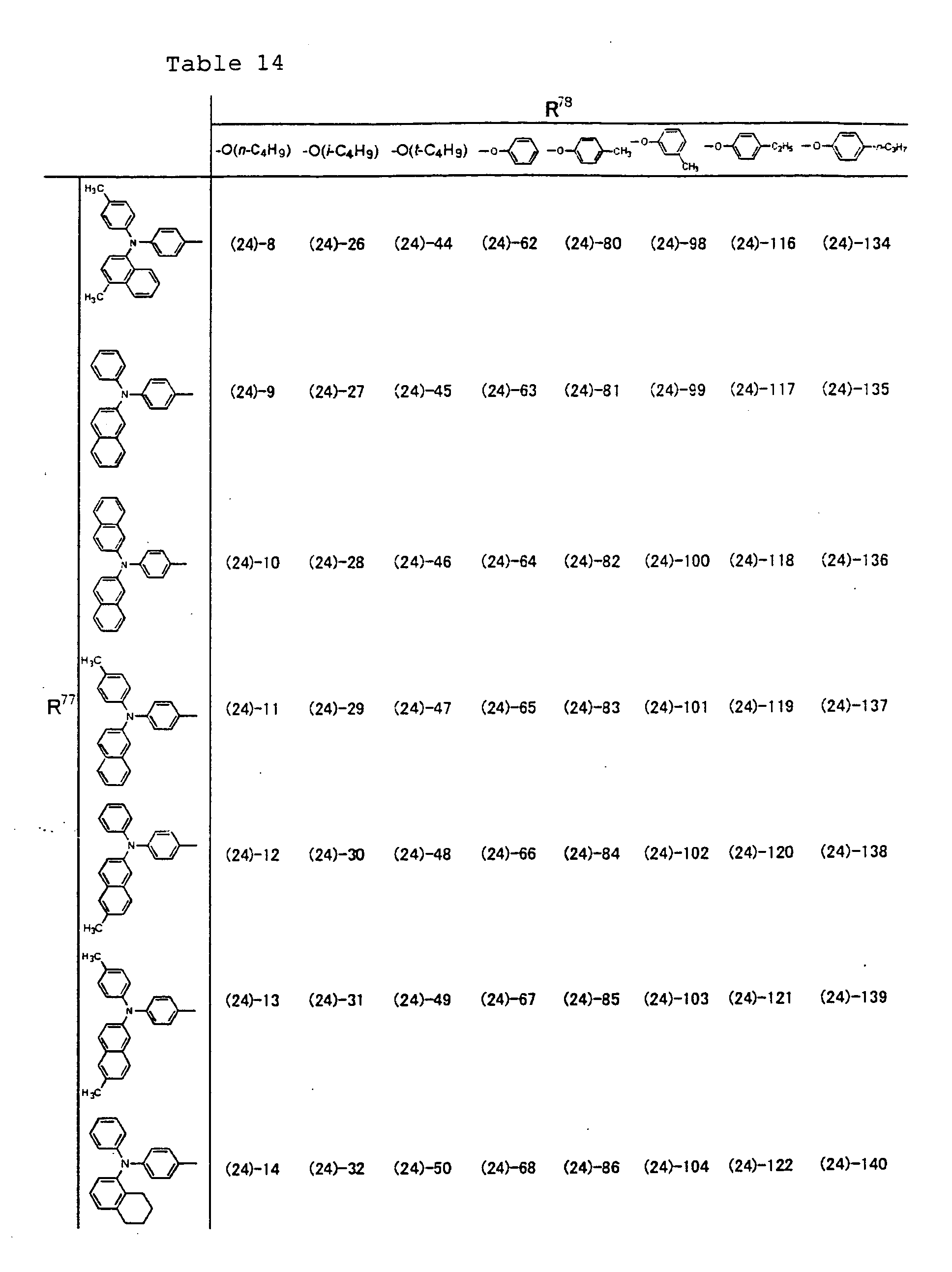
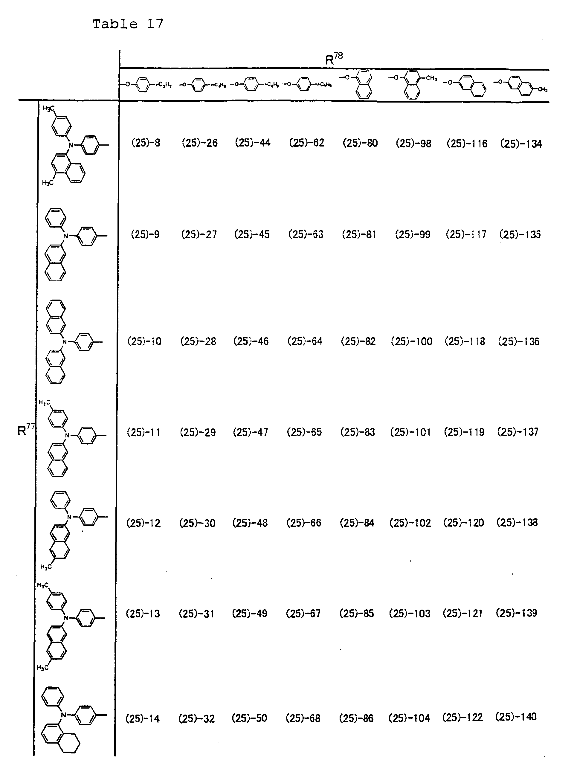
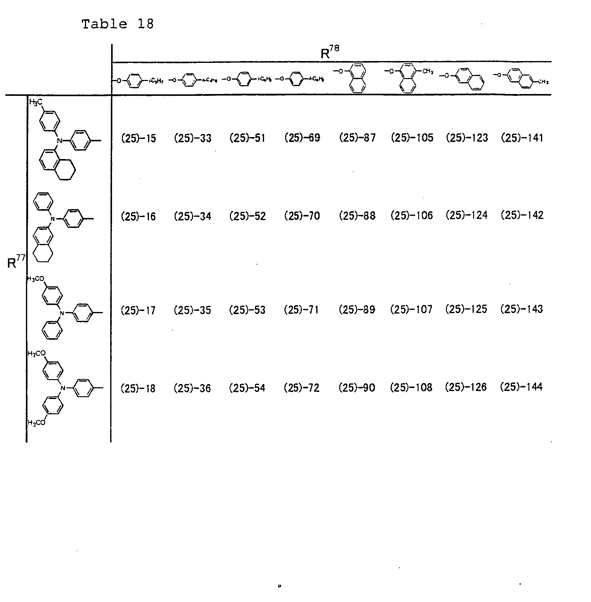
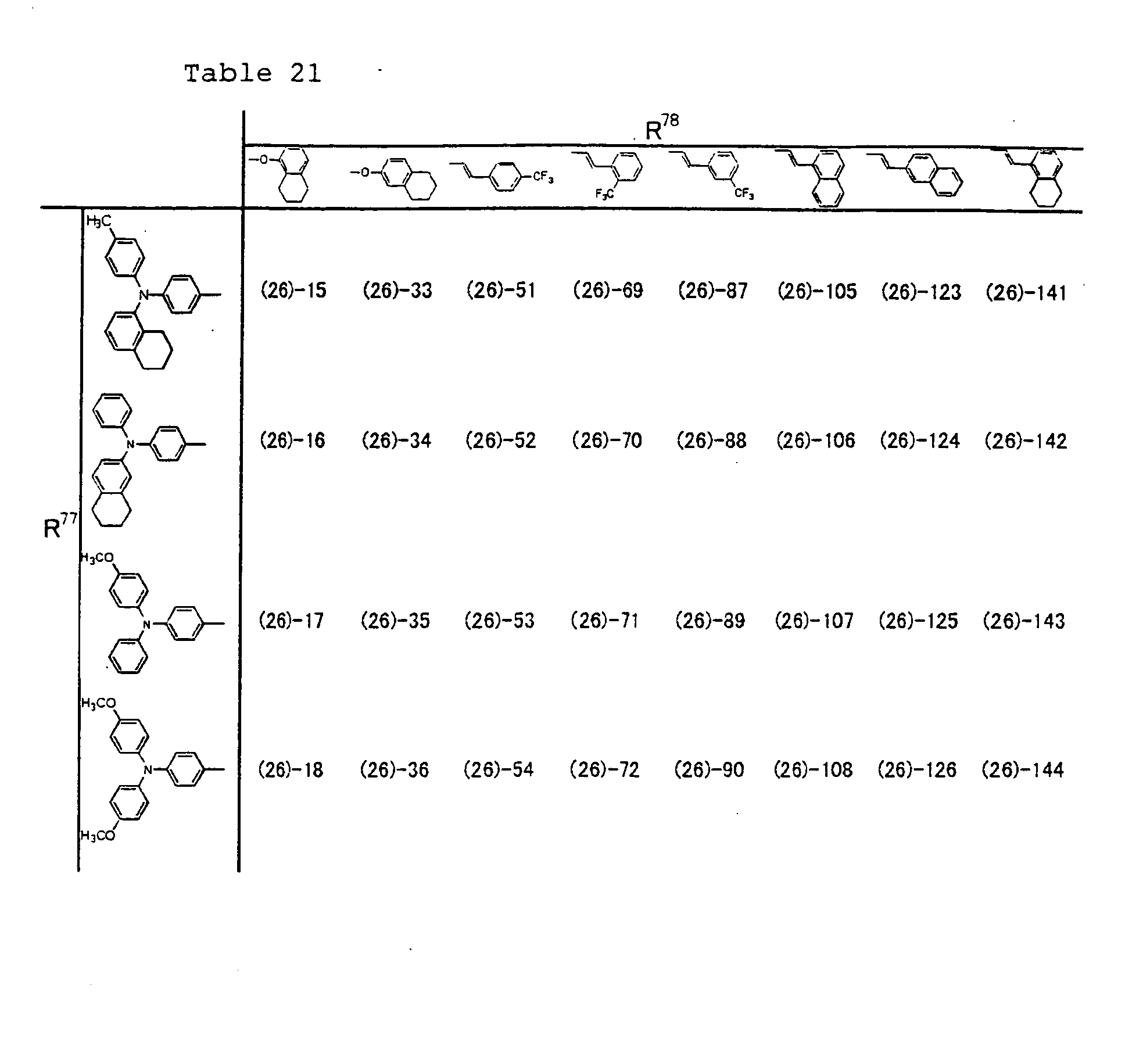
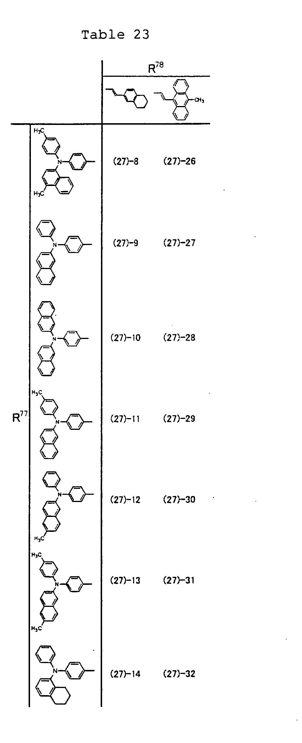
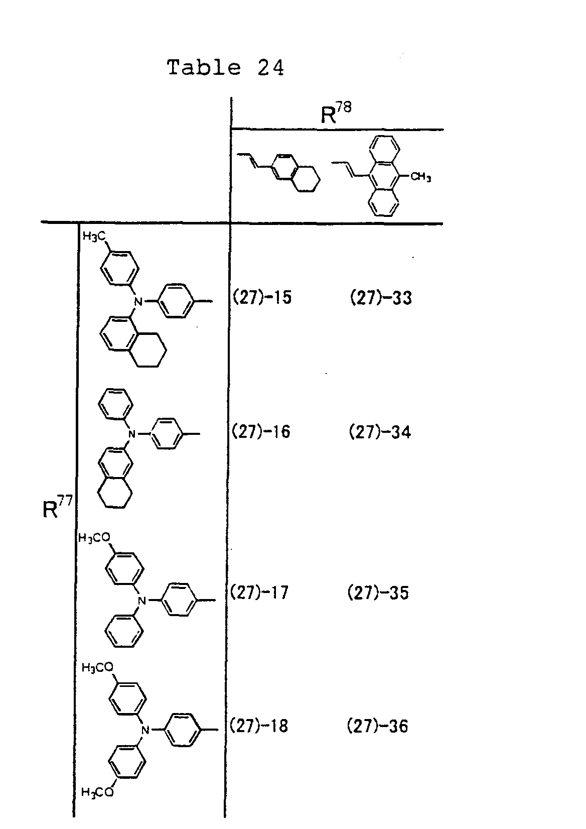
- aminostyrylnaphthalene compounds represented by the formulas (5) to (17), specifically the aminostyrylnaphthalene compounds shown above in Table 1 to Table 24 can be obtained.
- the present invention also provides various compounds suitable as synthesis intermediates for the compound according to the present invention.
- they include the phosphonate ester represented by the formula [C], especially the formula [V] and the phosphonium represented by the formula [D], especially the formula [VI], which is useful as a synthesis intermediate for the aminostyrylnaphthalene compound represented by the formula [A], especially the formula [I], [II] or [III].
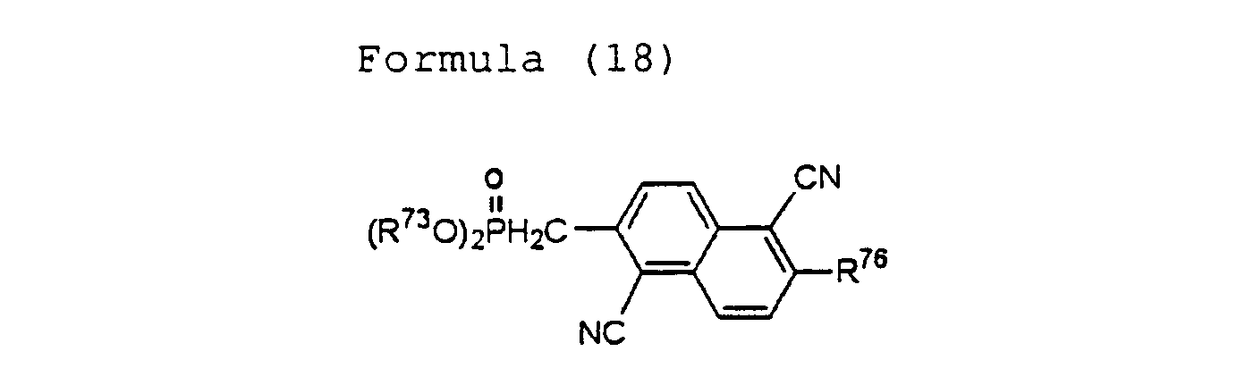
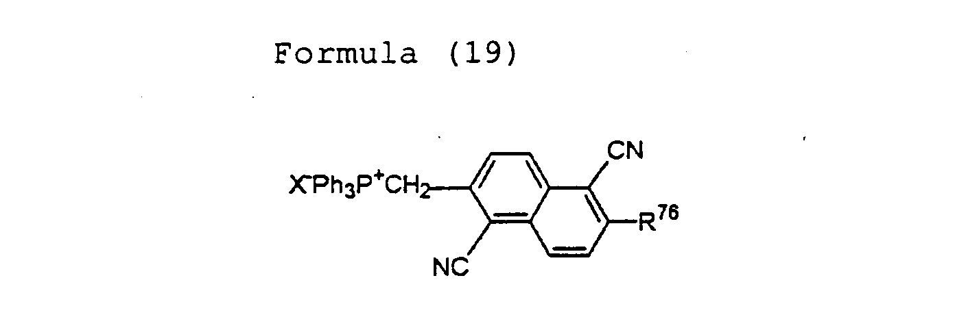
- the synthesis intermediate (hereinafter called “the synthesis intermediate 1 of the present invention") is specifically represented by the following formula (18) or (19): wherein R 73 , R 76 and X have the same meanings as defined above.
- the synthesis intermediate 1 of the present invention can be derived from a synthesis intermediate 2 as a precursor as will be described next.
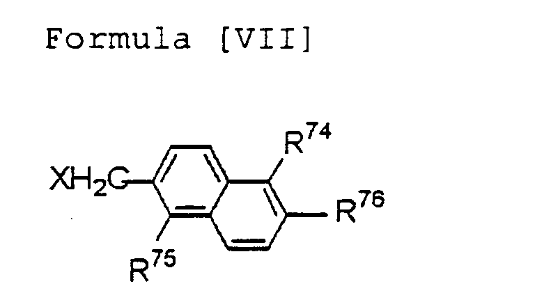
- the phosphonate ester represented by the formula [C], especially the formula [V] [for example, the formula (18)] or the phosphonium represented by the formula [D], especially the formula [VI] [for example, the formula (19)] can be obtained as a synthesis intermediate by reacting a halogenated aryl compound represented by the below-described formula [E], especially the formula [VII] with a trialkyl phosphite represented by the below-described formula [F], especially the formula [VIII] or triphenylphosphine (PPh 3 ).
- R 74 and R 75 may be the same or different, one of R 74 and R 75 represents a hydrogen atom, a cyano group, a nitro group, a trifluoromethyl group or a halogen atom, and the remaining one represents a hydrogen atom, a cyano group, a nitro group, a trifluoromethyl group or a halogen atom;
- R 76 represents a substituted or unsubstituted, saturated or unsaturated alkyl group (especially, a saturated or unsaturated alkyl group having 1 to 6 carbon atoms), a substituted or unsubstituted alicyclic hydrocarbon group, a substituted or unsubstituted aryl group, a substituted or unsubstituted alkoxyl group, a substituted or unsubstituted alicyclic hydrocarbyloxy group, or a substituted or unsubstituted aromatic hydrocarbyloxy group; and
- X represents a halogen
- the present invention also provides, as a synthesis intermediate for the synthesis intermediate 1, a halogenated aryl compound represented by the formula [E], especially the formula [VII] (hereinafter called "the synthesis intermediate 2 of the present invention”).
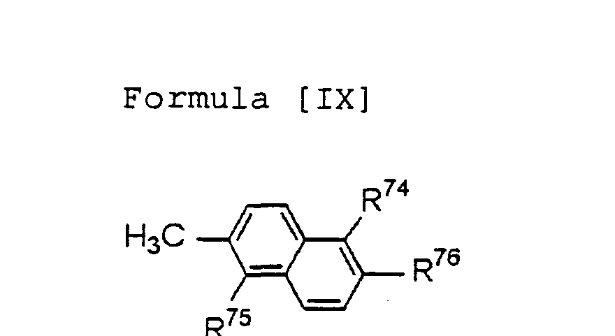
- the synthesis intermediate 2 of the present invention can be obtained by reacting a naphthalene compound represented by the following formula [G], especially the formula [IX] with an N-halogenated succinimide represented by the following formula [H] under irradiation of light.
- a naphthalene compound represented by the following formula [G], especially the formula [IX] with an N-halogenated succinimide represented by the following formula [H] under irradiation of light.
- a solvent such as carbon tetrachloride, chloroform, benzene or chlorobenzene
- a light source such as a high-pressure mercury lamp, low-pressure mercury lamp, xenon lamp, halogen lamp, sunlight or fluorescent lamp.
- R c , R d , R e , R f , R g , R h and R i have the same meanings as defined above.
- R 74 and R 75 may be the same or different, one of R 74 and R 75 represents a hydrogen atom, a cyano group, a nitro group, a trifluoromethyl group or a halogen atom, the remaining one of R 74 and R 75 represents a hydrogen atom, a cyano group, a nitro group, a trifluoromethyl group or a halogen atom, and R 76 represents a substituted or unsubstituted, saturated or unsaturated alkyl group (especially, a saturated or unsaturated alkyl group having 1 to 6 carbon atoms), a substituted or unsubstituted alicyclic hydrocarbon group, a substituted or unsubstituted aryl group, a substituted or unsubstituted alkoxyl group, a substituted
- reaction scheme 2 The reactions for obtaining the above-mentioned, respective synthesis intermediates 1 and 2 can be expressed, for example, by the following reaction scheme 2:
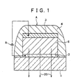
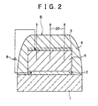
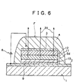
- FIG. 1 to FIG. 6 show organic electroluminescent devices according to various embodiments of the present invention, respectively.
- FIG. 1 shows a bottom-emitting organic electroluminescent device A, in which emitted light 20 transmits through an anode 2 and light reflected by a cathode 3 is also obtained as emitted light 20.
- FIG. 2 illustrates a surface-emitting organic electroluminescent device B, in which light reflected by an anode 2 is also obtained as emitted light 20 through a thin cathode 3 and the emitted light 20 can be observed from the side of a protective layer 4.
- numeral 1 indicates a substrate for forming the organic electroluminescent device. Glass, plastics or any other appropriate material is usable. When the organic electroluminescent device is used in combination with another display device, these devices can use a single substrate in common.
- the anode 2 is a transparent electrode and ITO (indium tin oxide), SnO 2 or the like can be used.
- an organic luminescent layer 5 contains the above-described aminostyrylnaphthalene compound of the present invention as a light emitting material.
- a multilayer structure of the luminescent layer 5 for obtaining the emitted light various known structures can be used.
- a material forming either a hole transport layer or an electron transport layer has light emitting property, for example, a structure with these transport layers stacked as thin films one over the other can be used.
- the present invention does not prevent one or both of a hole transport layer and an electron transport layer from using a structure, which is formed of thin films of plural materials stacked one over another, or a thin film of a composition, which has been obtained by mixing plural materials, to improve the performance of electron transportation within a range in which the objects of the present invention are satisfied.
- at least one fluorescent material may also be used in such a structure as having a thin film of the fluorescent material held between a hole transport layer and an electron transport layer or in such a structure as having the fluorescent material incorporated in a hole transport layer or an electron transport layer or in both of them.
- a thin film for controlling the transport of holes or electrons may also be included in the multilayer structure.
- the aminostyrylnaphthalene compound represented by the formula [A], especially the formula [I], [II] or [III] is equipped with both of electron transporting ability and hole transporting ability, the compound can be used as a mixed luminescent layer together with an electron transporting material or as a mixed luminescent layer together with a hole transporting material in the device structure. Further, a mixed layer with the compound contained therein can be used as a light emitting material in such a structure as having the mixed layer held between an electron transport layer and a hole transport layer.
- FIG. 1 and FIG. 2 each depicts the cathode 3.
- an electrode material it is possible to use an alloy or stacked structure of an active metal such as Li, Mg or Ca with a metal such as Ag, Al or In.
- a transmission-type organic electroluminescent device a light reflectance suited to its application purpose can be obtained by adjusting the thickness of its cathode.
- the protective film 4 has sealing property, and its effect can be enhanced by forming it into such a structure as covering the organic electroluminescent device in its entirety. Any suitable material can be used insofar as air tightness can be maintained.
- the organic layer may have an organic multilayer structure (single heterostructure) with a hole transport layer and an electron transport layer stacked one over the other, and as the material forming the hole transport layer or the electron transport layer, a mixed layer with the aminostyrylnaphthalene compound contained therein can be used.
- the organic layer may have an organic multilayer structure (double heterostructure) with a hole transport layer, a luminescent layer and an electron transport layer stacked one over another, and as the material forming the luminescent layer, a mixed layer with the aminostyrylnaphthalene compound contained therein can be used.
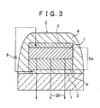
- FIG. 3 illustrates a bottom-emitting, organic electroluminescent device C of the single heterostructure, which has a multilayer structure formed of a light-transmitting anode 2, an organic layer 5a, and a cathode 3 stacked one over another on a light-transmitting substrate 1.
- the organic layer 5a is composed of a hole transport layer 6 and an electron transport layer 7.
- the multilayer structure is sealed with a protective layer 4.
- emitted light 20 of a predetermined wavelength is produced from an interface between the hole transport layer 6 and the electron transport layer 7.
- the emitted light can be observed from the side of the substrate 1.
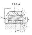
- FIG. 4 depicts a bottom-emitting organic electroluminescent device D of the double heterostructure, which has a multilayer structure formed of a light-transmitting anode 2, an organic layer 5b, and a cathode 3 stacked one over another on a light-transmitting substrate 1.
- the organic layer 5b is composed of a hole transport layer 10, a luminescent layer 11 and an electron transport layer 12.
- the multilayer structure is sealed with a protective layer 4.
- a light-transmitting material such as glass or plastics can be used as the substrate 1 as desired.
- the organic electroluminescent device is used in combination with another display device or when a plurality of multilayer structures as shown in FIG. 3 or FIG. 4 are arranged in the form of a matrix, for example, the substrate may be used in common.
- the devices C and D can each take either a transmission-type structure or a reflection-type structure.
- the anode 2 is a transparent electrode, and ITO, SnO 2 or the like can be used. Between the anode 2 and the hole transport layer 6 (or the hole transport layer 10), a thin film made of an organic material or an organometallic compound may be arranged to improve the charge injection efficiency.
- the protective layer 4 is formed of a conductive material such as a metal, the anode 2 may be provided on side walls thereof with insulating films, respectively.
- the organic layer 5a is formed of the hole transport layer 6 and electron transport layer 7 stacked together.
- the above-described aminostyrylnaphthalene compound may be incorporated in one or both of these transport layers to convert them into a luminescent, hole transport layer 6 and/or a luminescent, electron transport layer 7.
- the organic layer 5b is formed of the hole transport layer 10, the luminescent layer 11 with the above-described aminostyrylnaphthalene compound contained therein, and the electron transport layer 12, all of which are stacked together.
- the organic layer 5b can take a variety of other stacked structures. For example, one or both of the hole transport layer and electron transport layer may be modified into luminescent transport layer or layers.
- each hole transport layer may be formed of plural hole transporting materials stacked in layers one over another such that the hole transport layer is provided with improved hole transporting ability.
- the luminescent layer may be the luminescent, electron transport layer 7. Depending on a voltage impressed from a power supply 8, however, light may be emitted at the hole transport layer 6 or at its interfaces.
- the luminescent layer may also be either the electron transport 12 or the hole transport layer 10 in addition to the layer 11.
- a luminescent layer 11 which makes use of at least one fluorescent material, is held between a hole transport layer and an electron transport layer.
- the organic layer may be constructed into such a structure that the fluorescent material is incorporated in one or both of the hole transport layer and the electron transport layer. In each of these structures, it is possible to include a thin film, which can serve to control the transport of holes or electrons (for example, a hole blocking layer, exciton generating layer or the like), in the multilayer structure to improve its light emitting efficiency.
- each cathode 3 As a material for each cathode 3, an alloy of an active metal such as Li, Mg or Ca and a metal such as Ag, Al or In can be used. As an alternative, these metals may be used in a stacked structure. By selecting the thickness and material of the cathode as desired, an organic electroluminescent device suited for a specific application can be fabricated.
- an active metal such as Li, Mg or Ca
- a metal such as Ag, Al or In
- these metals may be used in a stacked structure.
- Each protective layer 4 acts as a sealing film.
- the protective layer in such a structure as covering the organic electroluminescent device in its entirety, the charge injection efficiency and light emitting efficiency can be improved.
- any desired material can be selected for the protective layer 4, including single metals and alloys of aluminum, gold, chromium and the like.
- FIG. 5 shows a surface-emitting, organic electroluminescent device E of the single heterostructure, which has a multilayer structure formed of an anode 2, an organic layer 5c and a transparent or translucent cathode 3 stacked one over another on a substrate 1.
- the organic layer 5c is composed of a hole transport layer 6 and an electron transport layer 7.
- the multilayer structure is sealed with a protective layer 4.
- emitted light 20 of a predetermined wavelength is produced from an interface between the hole transport layer 6 and the electron transport layer 7, and this emitted light is observed from the side of the cathode 3 or the protective layer 4.
- FIG. 6 illustrates a surface-emitting, organic electroluminescent device F, which has a multilayer structure formed of an anode 2, an organic layer 5d and a transparent or translucent cathode 3 stacked one over another on a substrate 1.
- the organic layer 5d is composed of a hole injection layer 9, a hole transport layer 10, a luminescent layer 11 and an electron transport layer 12.
- the multilayer structure is sealed with a protective layer 4.
- recombination of electrons and holes also takes place in the luminescent layer 11 in this organic electroluminescent device to form excitons, from which emission of light of a predetermined wavelength is produced.
- the substrate 1 can be formed by using a light-reflecting material such as Ag, Au, Al, Cr, In or the like or an alloy thereof as desired.
- a light-reflecting material such as Ag, Au, Al, Cr, In or the like or an alloy thereof as desired.
- the organic electroluminescent device is used in combination with another display device or when a plurality of multilayer structures as shown in FIG. 5 or FIG. 6 are arranged in the form of a matrix, the substrate may be used in common.
- the anode 2 on the substrate 1, on the other hand, is a reflective electrode. Ag, Au, Al, Cr or In or an alloy or the like thereof can be used. It is also possible to use ITO or the like by stacking the same. In view of film formability and reflectivity, its thickness may be set preferably at 50 nm or greater but not greater than 200 nm.
- the material of the substrate 1 is not limited to the above-described light-reflecting material, and a transparent or translucent material such as glass may be used.
- a hole injection layer 9 made of an inorganic material, an organic material or an organometallic compound may be arranged between the anode 2 and the hole transport layer 10 (or hole transport layer 6) to improve the charge injection efficiency.
- the protective layer 4 is formed of a conductive material such as a metal
- the anode 2 may be provided on side walls thereof with insulating films for insulation separation.
- the organic layer 5c in the organic electroluminescent device E is an organic layer formed of the hole transport layer 6 and the electron transport layer 7 stacked one over the other.
- One or both of these transport layers may be arranged as mixed layer or layers with above-described aminostyrylnaphthalene compound contained therein such that a light-emitting, hole transport layer 6 and/or electron transport layer 7 are formed.
- the organic layer 5d in the organic electroluminescent device F is an organic layer formed of the hole transport layer 10, the luminescent layer 11, which is formed of a mixture with the above-described aminostyrylnaphthalene compound contained therein, and the electron transport layer 12 stacked one over another.
- various multilayer structures can be adopted. For example, one or both of the hole transport layer and electron transport layer may be formed to emit light.
- the hole transport layer may be arranged as a hole transport layer formed of plural hole-transporting materials stacked in layers one over another.
- the luminescent layer may be the luminescent, electron transport layer 7. Depending on a voltage impressed from the power supply 8, however, light may be emitted at the hole transport layer 6 or at its interfaces.
- the luminescent layer may also be either the electron transport 12 or the hole transport layer 10 in addition to the layer 11.
- a luminescent layer 11 which makes use of at least one fluorescent material, is held between a hole transport layer and an electron transport layer.
- the organic layer may be constructed into such a structure that the fluorescent material is incorporated in one or both of the hole transport layer and the electron transport layer. In each of these structures, it is possible to include a thin film, which can serve to control the transport of holes or electrons (for example, a hole blocking layer, exciton generating layer or the like), in the multilayer structure to improve its light emitting efficiency.
- each cathode 3 As a material for each cathode 3, an alloy of an active metal such as Li, Mg or Ca and a metal such as Ag, Al or In can be used. As an alternative, these metals may be used in a stacked structure.
- an organic electroluminescent device suited for a specific application can be fabricated. Desirably, however, the thickness of the cathode may range from 0.5 to 15 nm with a range of from 0.5 to 5 nm or so being more desired.
- Each protective layer 4 acts as a sealing film.
- the protective layer in such a structure as covering the organic electroluminescent device in its entirety, the charge injection efficiency and light emitting efficiency can be improved.
- any desired material can be selected for the protective layer 4, including single metals, alloys, compounds and the like such as aluminum, gold, chromium, silicon oxide, silicon nitride and the like.
- the luminescent layer is held between the anode and the cathode, and emitted light causes multiple interference between the anode and the cathode.
- optical characteristics of the anode and cathode such as their reflectivities and transmittances, and the thickness of the organic layer held between the anode and the cathode
- multiple interference effect can be used positively such that the wavelength of light emitted from each of the devices E, F can be controlled. This makes it possible to improve the chromaticy of light to be emitted.
- a current to be impressed to each of the above-described organic electroluminescent devices is generally a direct current, but instead, a pulsed current or an alternating current may be used. Neither the current value nor the voltage value are particularly limited insofar they fall within such ranges that the device would remain undamaged. In view of the power consumption and service life of the organic electroluminescent device, however, it is desired to make the organic electroluminescent device efficiently emit light with as smaller electric energy as possible.
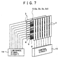
- FIG. 7 shows an illustrative construction of a flat display making use of an organic electroluminescent device according to the present invention.
- an organic layer 5 (5a, 5b) which can emit primaries of red (R), green (G) and blue (B) are arranged between cathodes 3 and anodes 2.
- the cathodes 3 and anodes 2 can be arranged in the form of stripes crossing each other.
- a luminance signal circuit 14 and a control circuit 15 equipped with a built-in register signal voltages are selectively impressed to the cathodes 3 and anodes 2 such that light is emitted from the organic layers at positions (pixels) where the selected cathodes 3 and anodes 2 intersect with each other in a single matrix system or active matrix system.
- FIG. 7 shows by way of example an 8 ⁇ 3 RGB single matrix, in which stacked layers 5 each formed of a hole transport layer and at least one of a luminescent layer and electron transport layer are arranged between the cathodes 3 and the anodes 2 (see FIG. 3, FIG. 4, FIG. 5 or FIG. 6).
- the cathodes and anodes are constructed such that they are patterned in the form of stripes and are arranged at right angles relative to each other in the form of a matrix and, by the control circuit 15 equipped with the built-in shift register and the luminance signal circuit 14, signal voltages are impressed in time sequence to emit light at their crossing positions.
- EL devices of such a construction can also be used as picture reproducers, to say nothing of displays for characters, signs and the like.
- the striped patterns of the cathodes 3 and anodes 2 can be arranged for each of red (R), green (G) and blue (B) to construct a multicolor or full-color, full solid-state flat panel display.
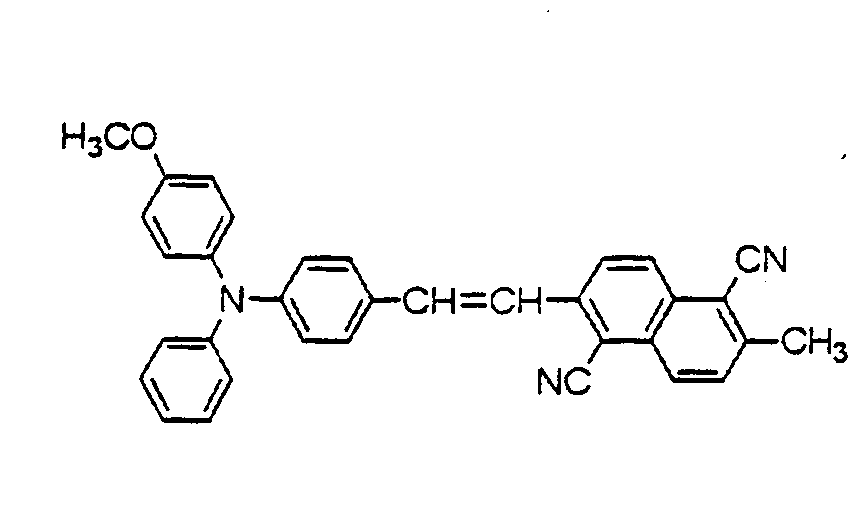
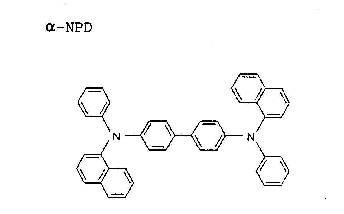
- a bottom-emitting, organic electroluminescent device of the single heterostructure was fabricated by using the compound of the above-described structural formula (20)-17 as a luminescent, electron transport layer and 4,4'-bis[N,N'-di(1-naphthyl)-N,N'-diphenyl]biphenyldiamine ( ⁇ -NPD) of the below-described structural formula as a hole transport layer.
- a 30 mm ⁇ 30 mm glass substrate with a 100-nm thick ITO anode formed on a surface thereof was set in a vacuum evaporation system.
- a metal mask having a plurality of 2.0 mm ⁇ 2.0 mm unit openings formed therethrough was disposed as an evaporation mask in a proximity of the substrate, and by vacuum evaporation, ⁇ -NPD as a hole transporting material was deposited to a thickness of 140 nm under a vacuum of 10 -4 Pa or lower.
- the compound of the above structural formula (20)-35 was deposited as a luminescent, electron transporting material to a thickness of 55 nm in contact with the hole transport layer.
- the deposition rate was set at 0.2 nm/sec in each of the above vacuum evaporation steps.
- Mg and Ag were adopted as cathode materials. By vacuum evaporation, they were also deposited at deposition rates of 1 nm/sec to thicknesses of 50 nm (Mg film) and 150 nm (Ag film), respectively, to form a stacked film of Mg and Ag, so that an organic electroluminescent device was fabricated as illustrated in FIG. 3.
- the organic electroluminescent device was left over for 1 month under a nitrogen atmosphere, but no degradation was observed on the device. Further, the organic electroluminescent device was subjected to forced degradation at an initial luminance of 100 cd/m 2 by applying a current at a constant value to continuously emit light. It took 800 hours until the luminance dropped to half.
- a bottom-emitting, organic electroluminescent device of the double heterostructure was fabricated by using the above-described ⁇ -NPD as a hole transport layer and the compound of the above-described structural formula (20)-17 as a luminescent layer.
- a 30 mm ⁇ 30 mm glass substrate with a 100-nm thick ITO anode formed on a surface thereof was set in a vacuum evaporation system.
- a metal mask having a plurality of 2.0 mm ⁇ 2.0 mm unit openings formed therethrough was disposed as an evaporation mask in a proximity of the substrate, and by vacuum evaporation, ⁇ -NPD as a hole transporting material was deposited to a thickness of 140 nm under a vacuum of 10 -4 Pa or lower.
- the compound of the above structural formula (20)-35 was deposited as a light emitting material to a thickness of 40 nm in contact with the hole transport layer.
- the deposition rate was set at 0.2 nm/sec in each of the above vacuum evaporation steps.
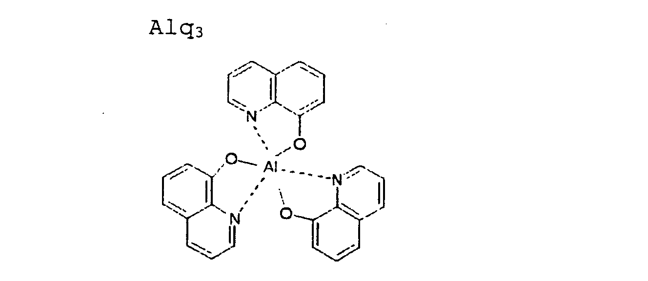
- As an electron transport layer tris(8-hydroxyquinoline)aluminum (Alq 3 ) of the below-described structural formula was deposited further in contact with the luminescent layer.
- the electron transport layer made of Alq 3 was deposited to a thickness of 50 nm.
- the deposition rate was set at 0.2 nm/sec.
- Mg and Ag were adopted as cathode materials. By vacuum evaporation, they were also deposited at deposition rates of 1 nm/sec to thicknesses of 50 nm (Mg film) and 150 nm (Ag film), respectively, to form a stacked film of Mg and Ag, so that an organic electroluminescent device was fabricated as illustrated in FIG. 4.
- the organic electroluminescent device was left over for 1 month under a nitrogen atmosphere, but no degradation was observed on the device. Further, the organic electroluminescent device was subjected to forced degradation at an initial luminance of 100 cd/m 2 by applying a current at a constant value to continuously emit light. It took 1,300 hours until the luminance dropped to half.
- a surface-emitting, organic electroluminescent device was fabricated by using, as a light-emitting, electron transport layer, a mixed layer of the compound of the above-described structural formula (20)-17 and Alq 3 of the above-described structural formula.
- a 30 mm ⁇ 30 mm glass substrate was set in a vacuum evaporation system.
- the glass substrate carried on a surface thereof anodes composed of a 100-nm thick silver alloy and a 10-nm thick ITO formed as a film on the silver alloy.
- a metal mask having a plurality of 2.0 mm ⁇ 2.0 mm unit openings formed therethrough was disposed as an evaporation mask in a proximity of the substrate.
- 2-TNATA of the below-described structural formula was deposited as a hole injection layer, for example, to a thickness of 20 nm, and over the hole injection layer, ⁇ -NPD was further deposited as a hole transport layer, for example, to a thickness of 43 nm.
- the deposition rate was set at 0.1 nm/sec in each of the above vacuum evaporation steps.
- the above-described compound of the structural formula (20)-17 and as an electron transporting material, Alq 3 were deposited as a mixed layer at an evaporation rate ratio of 1:1 in contact with the hole transport layer.
- the thickness of the electron transport layer (which also serves as a luminescent layer) made of the compound of the structural formula (20)-17 and Alq 3 was set, for example, at 30 nm, and their deposition rates were each set at 0.2 nm/sec.
- Alq 3 was deposited further as an electron transport layer, for example, to a thickness of 36 nm.
- a mixed film of Mg and Ag was adopted as a cathode material.
- the mixed film was also formed, for example, to a thickness of 12 nm while controlling the mixing ratio of Mg to Ag at 5:1.
- an organic electroluminescence device was fabricated as illustrated in FIG. 6.
- the organic electroluminescent device was left over for 1 month under a nitrogen atmosphere, but no degradation was observed on the device. Further, the organic electroluminescent device was subjected to forced degradation at an initial luminance of 100 cd/m 2 by applying a current at a constant value to continuously emit light. It took 2,050 hours until the luminance dropped to half.
- a Witting-Horner reagent (30) (7.00 g, 20.3 mmol) was suspended in methanol (100 mL) over an ice bath. Under stirring, sodium methoxide (1.20 g, 22.2 mmol) was added little by little, followed by stirring for 30 minutes. 4-[N,N'-(4-methyldiphenyl)]aminobenzaldehyde (29) (5.60 g, 18.5 mmol) was added in two portions, and the temperature of the resulting mixture was allowed to rise, as was, from 0°C to room temperature, at which the mixture was stirred for 6 hours.
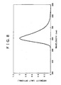
- a solution of the product in THF had a visible absorption maximum at 437 nm and a fluorescence maximum wavelength at 612 nm.
- the relative fluorescence quantum yield of the product in dioxane was 0.97, that is, very high.
- the aminostyrylnaphthalene compound represented by the formula [A] is excellent in light emitting properties, and moreover, shows amorphous properties advantageous for film formability by vacuum deposition or the like and also durability.
- the use of the aminostyrylnaphthalene compound makes it possible to provide an organic electroluminescent device capable of producing high-luminance and stable emission of light at an optimal wavelength.
Landscapes
- Chemical & Material Sciences (AREA)
- Organic Chemistry (AREA)
- Engineering & Computer Science (AREA)
- Materials Engineering (AREA)
- Physics & Mathematics (AREA)
- Spectroscopy & Molecular Physics (AREA)
- Life Sciences & Earth Sciences (AREA)
- Biochemistry (AREA)
- General Health & Medical Sciences (AREA)
- Molecular Biology (AREA)
- Health & Medical Sciences (AREA)
- Organic Low-Molecular-Weight Compounds And Preparation Thereof (AREA)
- Electroluminescent Light Sources (AREA)
Abstract

Description






















a 4-(N,N-diarylamino)benzaldehyde represented by the following formula (29) and at least one of a phosphonate ester represented by the following formula (30) and a phosphonium represented by the following formula (31) are subjected to condensation.



P (ORi) 3
P(OR73) 3




Claims (26)
- An organic electroluminescent device comprising an anode, a cathode, and an organic layer arranged between said anode and said cathode, wherein at least a part of said organic layer comprises at least one aminostyrylnaphthalene compound represented by the following formula [A]:wherein:
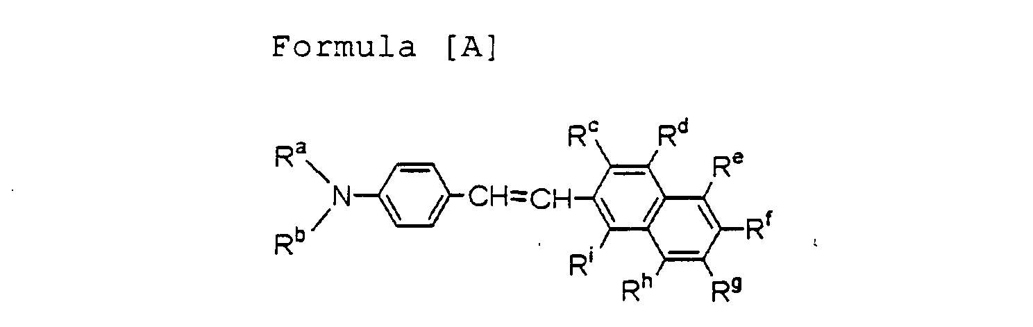 Ra and Rb may be the same or different and each independently represents a substituted or unsubstituted aryl group,Rc, Rd, Re, Rg, Rh and Ri may be the same or different, at least one of Rc, Rd, Re, Rg, Rh and Ri independently represents a hydrogen atom, a cyano group, a nitro group, a trifluoromethyl group or a halogen atom, and the remaining one or ones of Rc, Rd, Re, Rg, Rh and Ri, if any, are each a hydrogen atom, a cyano group, a nitro group, a trifluoromethyl group or a halogen atom, andRf represents a substituted or unsubstituted, saturated or unsaturated alkyl group, a substituted or unsubstituted alicyclic hydrocarbon group, a substituted or unsubstituted aryl group, a substituted or unsubstituted alkoxyl group, a substituted or unsubstituted alicyclic hydrocarbyloxy group or a substituted or unsubstituted aromatic hydrocarbyloxy group.
 - The organic electroluminescent device according to claim 1, wherein at least said part of said organic layer comprises at least one aminostyrylnaphthalene compound represented by the following formula [I], [II] or [III]:wherein:
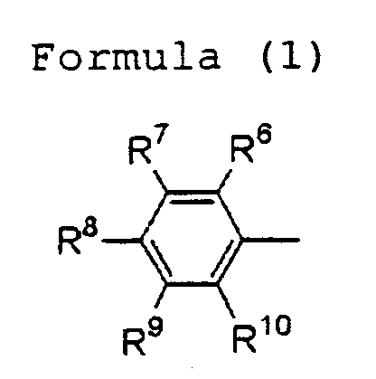
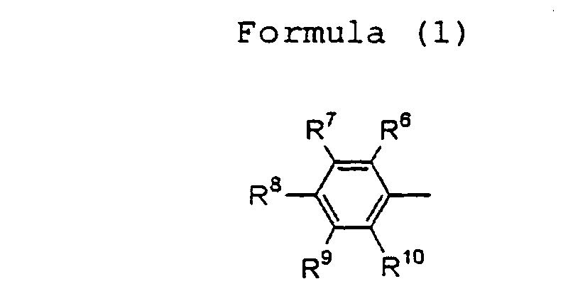
 R1 and R2 may be the same or different and each independently represents a phenyl group represented by the following formula (1):wherein R6, R7, R8, R9 and R10 may be the same or different, at least one of R6 to R10 represents a hydrogen atom, a saturated or unsaturated hydrocarbon group having at least one carbon atom with a proviso that, when at least two adjacent ones of R6 to R10 each represents a saturated or unsaturated hydrocarbon group having at least one carbon atom, at least said two adjacent ones of R6 to R10 may be fused together to form a ring, a saturated or unsaturated hydrocarbyloxy group having at least one carbon atom, a saturated or unsaturated hydrocarbylamino group having at least one carbon atom, a trifluoromethyl group, a cyano group or a halogen atom, and the remaining one or ones of R6 to R10, if any, are each a hydrogen atom, a saturated or unsaturated hydrocarbon group having at least one carbon atom with a proviso that, when at least two adjacent ones of R6 to R10 each represents a saturated or unsaturated hydrocarbon group having at least one carbon atom, at least said two adjacent ones of R6 to R10 may be fused together to form a ring, a saturated or unsaturated hydrocarbyloxy group having at least one carbon atom, a saturated or unsaturated hydrocarbylamino group having at least one carbon atom, a trifluoromethyl group, a cyano group or a halogen atom,
 R3 and R4 may be the same or different, one of R3 and R4 represents a hydrogen atom, a cyano group, a nitro group, a trifluoromethyl group or a halogen atom, and the remaining one represents a hydrogen atom, a cyano group, a nitro group, a trifluoromethyl group or a halogen atom, andR5 represents a substituted or unsubstituted, saturated or unsaturated alkyl group, a substituted or unsubstituted, alicyclic hydrocarbon group, a substituted or unsubstituted aryl group, a substituted or unsubstituted alkoxyl group, a substituted or unsubstituted, alicyclic hydrocarbyloxy group, or a substituted or unsubstituted, aromatic hydrocarbyloxy group.wherein:
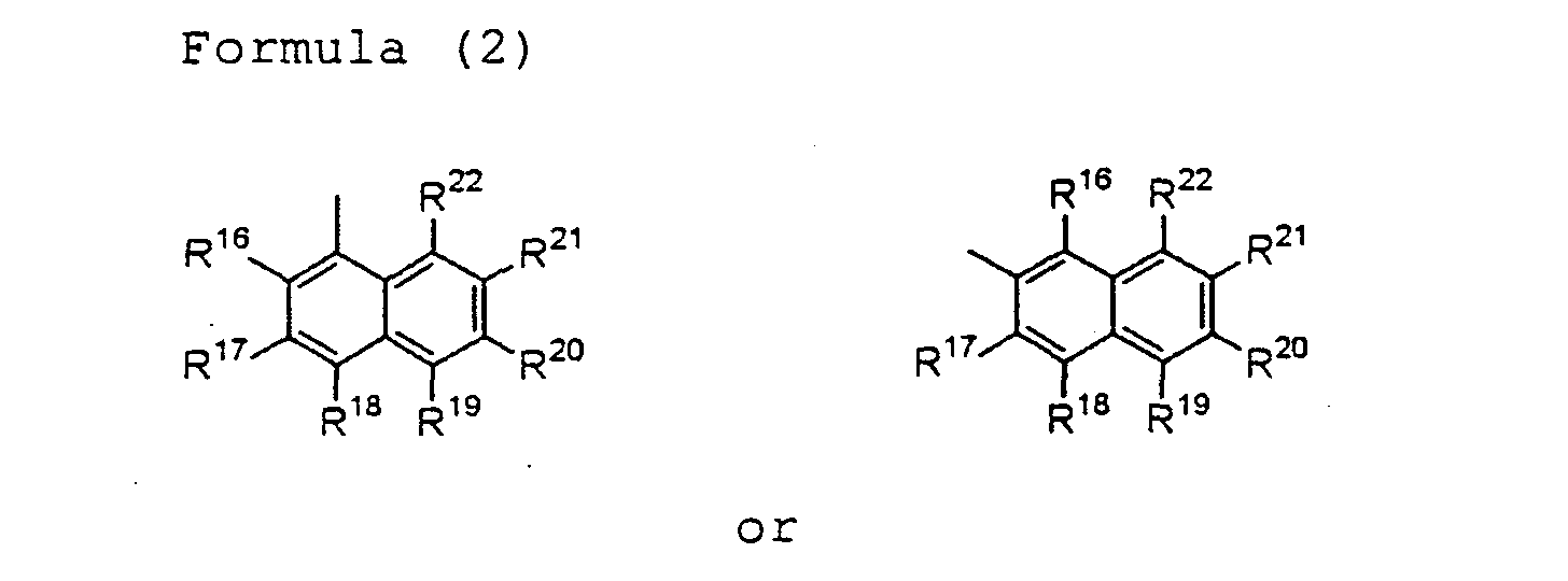
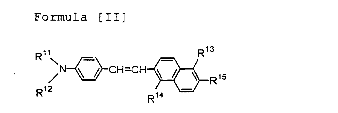 R11 and R12 may be the same or different and each independently represents a naphthyl group represented by the following formula (2):wherein R16 , R17, R18, R19 , R20, R21 and R22 may be the same or different, at least one of R16 to R22 represents a hydrogen atom, a saturated or unsaturated hydrocarbon group having at least one carbon atom, a saturated or unsaturated hydrocarbyloxy group having at least one carbon atom, a saturated or unsaturated hydrocarbylamino group having at least one carbon atom, a trifluoromethyl group, a cyano group or a halogen atom, and the remaining one or ones of R16 to R22, if any, are each a hydrogen atom, a saturated or unsaturated hydrocarbon group having at least one carbon atom, a saturated or unsaturated hydrocarbyloxy group having at least one carbon atom, a saturated or unsaturated hydrocarbylamino group having at least one carbon atom, a trifluoromethyl group, a cyano group or a halogen atom,
 R13 and R14 may be the same or different, one of R13 and R14 represents a hydrogen atom, a cyano group, a nitro group, a trifluoromethyl group or a halogen atom, and the remaining one represents a hydrogen atom, a cyano group, a nitro group, a trifluoromethyl group or a halogen atom, andR15 represents a substituted or unsubstituted, saturated or unsaturated alkyl group, a substituted or unsubstituted, alicyclic hydrocarbon group, a substituted or unsubstituted aryl group, a substituted or unsubstituted alkoxyl group, a substituted or unsubstituted, alicyclic hydrocarbyloxy group, or a substituted or unsubstituted, aromatic hydrocarbyloxy group.wherein:
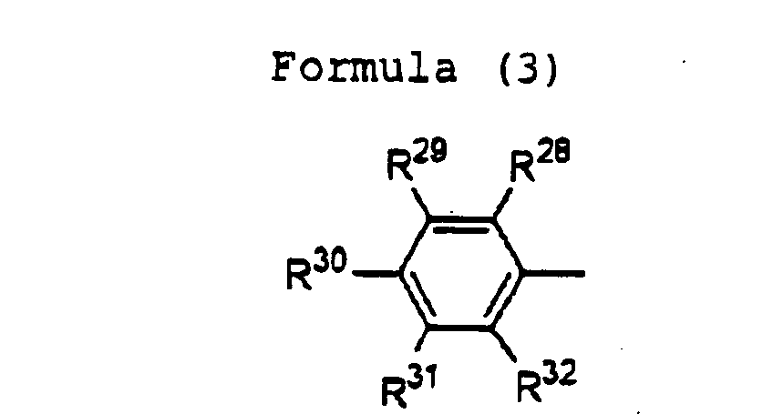
 R23 is a phenyl group represented by the following formula (3):wherein R28, R29, R30, R31 and R32 may be the same or different, at least one of R28 to R32 represents a hydrogen atom, a saturated or unsaturated hydrocarbon group having at least one carbon atom with a proviso that, when at least two adjacent ones of R29 to R32 each represents a saturated or unsaturated hydrocarbon group having at least one carbon atom, at least said two adjacent ones of R29 to R32 may be fused together to form a ring, a hydrocarbyloxy group having at least one carbon atom, a hydrocarbylamino group having at least one carbon atom, a trifluoromethyl group, a cyano group or a halogen atom, and the remaining one or ones of R28 to R32, if any, are each a hydrogen atom, a saturated or unsaturated hydrocarbon group having at least one carbon atom with a proviso that, when at least two adjacent ones of R28 to R32 each represents a saturated or unsaturated hydrocarbon group having at least one carbon atom, at least said two adjacent ones of R28 to R32 may be fused together to form a ring, a saturated or unsaturated hydrocarbyloxy group having at least one carbon atom, a saturated or unsaturated hydrocarbylamino group having at least one carbon atom, a trifluoromethyl group, a cyano group or a halogen atom,
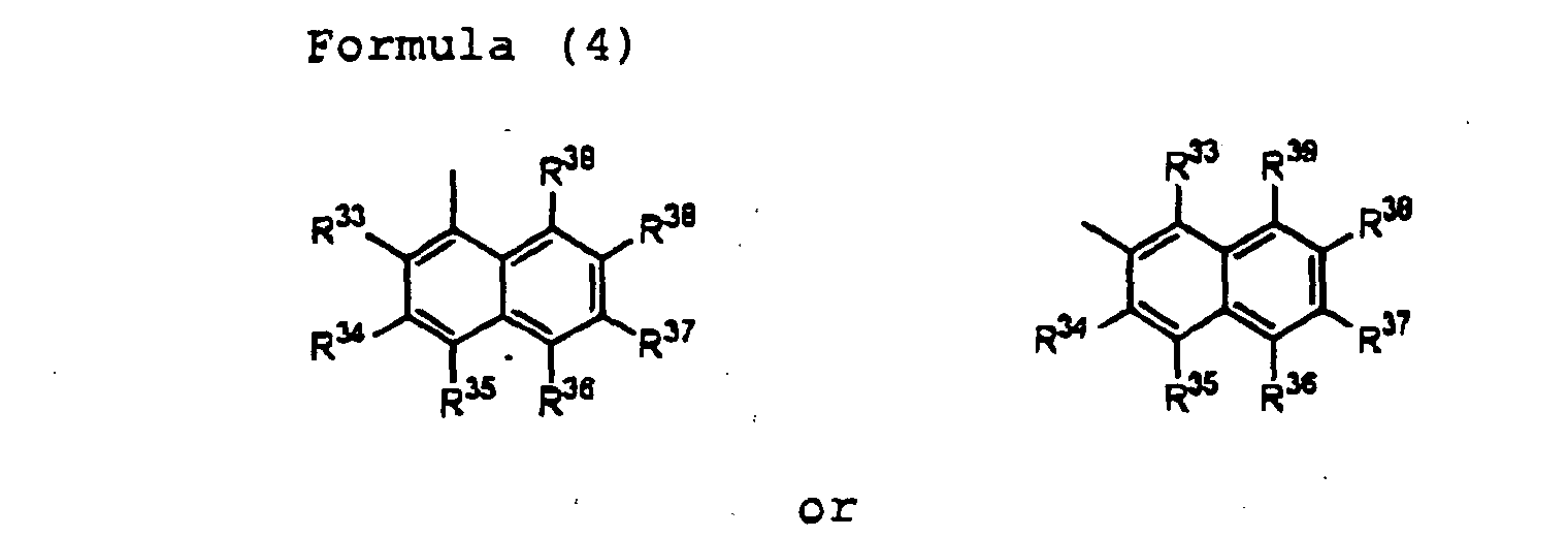
 R24 represents a naphthyl group represented by the following formula (4):wherein R33, R34, R35, R36, R37, R38 and R39 may be the same or different, at least one of R33 to R39 represents a hydrogen atom, a saturated or unsaturated hydrocarbon group having at least one carbon atom, a saturated or unsaturated hydrocarbyloxy group having at least one carbon atom, a saturated or unsaturated hydrocarbylamino group having at least one carbon atom, a trifluoromethyl group, a cyano group or a halogen atom, and the remaining one or ones of R33 to R39, if any, are each a hydrogen atom, a saturated or unsaturated hydrocarbon group having at least one carbon atom, a saturated or unsaturated hydrocarbyloxy group having at least one carbon atom, a saturated or unsaturated hydrocarbylamino group having at least one carbon atom, a trifluoromethyl group, a cyano group or a halogen atom,
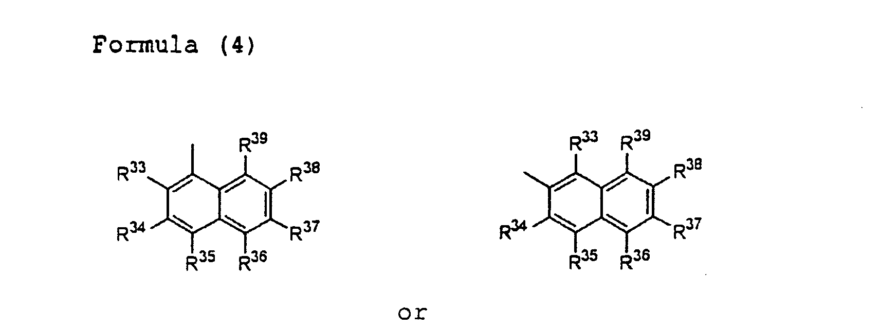 R25 and R26 may be the same or different, one of R25 and R26 represents a hydrogen atom, a cyano group, a nitro group, a trifluoromethyl group or a halogen atom, and the remaining one represents a hydrogen atom, a cyano group, a nitro group, a trifluoromethyl group or a halogen atom, andR27 represents a substituted or unsubstituted, saturated or unsaturated alkyl group, a substituted or unsubstituted, alicyclic hydrocarbon group, a substituted or unsubstituted aryl group, a substituted or unsubstituted alkoxyl group, a substituted or unsubstituted, alicyclic hydrocarbyloxy group, or a substituted or unsubstituted, aromatic hydrocarbyloxy group.
 - The organic electroluminescent device according to claim 1, wherein said organic layer is in a form of an organic multilayer structure comprising a hole transport layer and an electron transport layer stacked one over the other, and at least said electron transport layer in said organic layer comprises at least said one aminostyrylnaphthalene compound.
- The organic electroluminescent device according to claim 1, wherein said organic layer is in a form of an organic multilayer structure comprising a hole transport layer and an electron transport layer stacked one over the other, and at least said hole transport layer in said organic layer comprises at least said one aminostyrylnaphthalene compound.
- The organic electroluminescent device according to claim 1, wherein said organic layer is in a form of an organic multilayer structure comprising a hole transport layer, a luminescent layer and an electron transport layer stacked one over another, and at least said luminescent layer in said organic layer comprises at least said one aminostyrylnaphthalene compound.
- The organic electroluminescent device according to claim 2, wherein said aminostyrylnaphthalene compound is represented by the following formula (5), (6), (7), (8), (9), (10), (11), (12), (13), (14), (15), (16) or (17):wherein R40 represents a saturated or unsaturated alkyl group having 1 to 6 carbon atoms or a substituted or unsubstituted aryl group, and R41 has the same meaning as R5.
 wherein R42 and R43 may be the same or different and each independently represents a saturated or unsaturated alkyl group having 1 to 6 carbon atoms or a substituted or unsubstituted aryl group, and R44 has the same meaning as R5.
 wherein R45 represents a saturated or unsaturated alkyl group having 1 to 6 carbon atoms or a substituted or unsubstituted aryl group, and R46 has the same meaning as R27.
 wherein R47 and R48 may be the same or different, one of R47 and R48 represents a saturated or unsaturated alkyl group having 1 to 6 carbon atoms or a substituted or unsubstituted aryl group, the remaining one of R43 and R48 represents a saturated or unsaturated alkyl group having 1 to 6 carbon atoms or a substituted or unsubstituted aryl group, and R49 has the same meaning as R27.
 wherein R50 represents a saturated or unsaturated alkyl group having 1 to 6 carbon atoms or a substituted or unsubstituted aryl group, and R51 has the same meaning as R27.
 wherein R52 and R53 may be the same or different, one of R52 and R53 represents a saturated or unsaturated alkyl group having 1 to 6 carbon atoms or a substituted or unsubstituted aryl group, the remaining one of R52 and R53 represents a saturated or unsaturated alkyl group having 1 to 6 carbon atoms or a substituted or unsubstituted aryl group, and R54 has the same meaning as R27 .
 wherein R55 represents a saturated or unsaturated alkyl group having 1 to 6 carbon atoms or a substituted or unsubstituted aryl group, and R56 has the same meaning as R5.
 wherein R57 represents a saturated or unsaturated alkyl group having 1 to 6 carbon atoms or a substituted or unsubstituted aryl group, and R58 has the same meaning as R5.
 wherein R59 represents a saturated or unsaturated alkyl group having 1 to 6 carbon atoms or a substituted or unsubstituted aryl group, and R60 has the same meaning as R5.
 wherein R61 represents a saturated or unsaturated alkyl group having 1 to 6 carbon atoms or a substituted or unsubstituted aryl group, and R62 has the same meaning as R15.
 wherein R63 and R64 may be the same or different, one of R63 and R64 represents a saturated or unsaturated alkyl group having 1 to 6 carbon atoms or a substituted or unsubstituted aryl group, the remaining one of R63 and R64 represents a saturated or unsaturated alkyl group having 1 to 6 carbon atoms or a substituted or unsubstituted aryl group, and R65 has the same meaning as R15 .
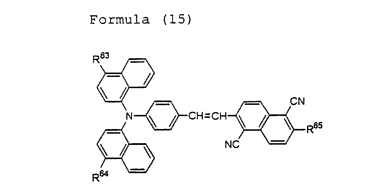 wherein R66 represents a saturated or unsaturated alkyl group having 1 to 6 carbon atoms or a substituted or unsubstituted aryl group, and R67 has the same meaning as R15.
 wherein R68 and R69 may be the same or different, one of R68 and R69 represents a saturated or unsaturated alkyl group having 1 to 6 carbon atoms or a substituted or unsubstituted aryl group, the remaining one of R68 and R69 represents a saturated or unsaturated alkyl group having 1 to 6 carbon atoms or a substituted or unsubstituted aryl group, and R70 has the same meaning as R15.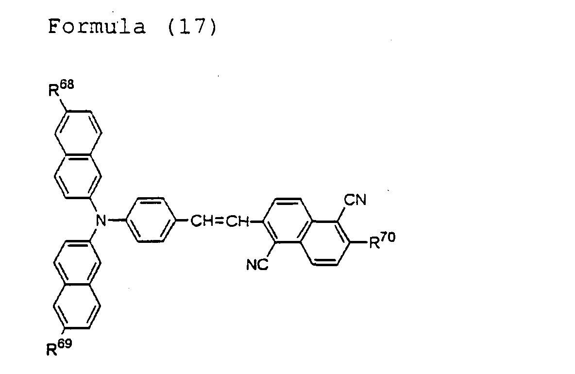
- An aminostyrylnaphthalene compound represented by the following formula [A]:wherein:
 Ra and Rb may be the same or different and each independently represents a substituted or unsubstituted aryl group,Rc, Rd, Re, Rg, Rh and Ri may be the same or different, at least one of Rc, Rd, Re, Rg, Rh and Ri independently represents a hydrogen atom, a cyano group, a nitro group, a trifluoromethyl group or a halogen atom, and the remaining one or ones of Rc, Rd, Re, Rg, Rh and Ri, if any, are each a hydrogen atom, a cyano group, a nitro group, a trifluoromethyl group or a halogen atom, andRf represents a substituted or unsubstituted, saturated or unsaturated alkyl group, a substituted or unsubstituted alicyclic hydrocarbon group, a substituted or unsubstituted aryl group, a substituted or unsubstituted alkoxyl group, a substituted or unsubstituted alicyclic hydrocarbyloxy group or a substituted or unsubstituted aromatic hydrocarbyloxy group.
 - The aminostyrylnaphthalene compound according to claim 7, which is represented by the following formula [I], [II] or [III]:wherein:
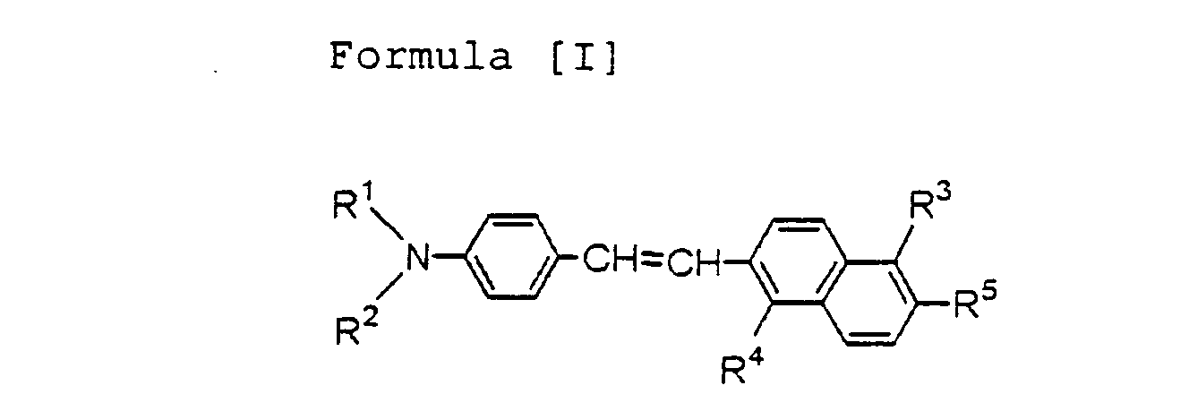 R1 and R2 may be the same or different and each independently represents a phenyl group represented by the following formula (1):wherein R6, R7, R8, R9 and R10 may be the same or different, at least one of R6 to R10 represents a hydrogen atom, a saturated or unsaturated hydrocarbon group having at least one carbon atom with a proviso that, when at least two adjacent ones of R6 to R10 each represents a saturated or unsaturated hydrocarbon group having at least one carbon atom, at least said two adjacent ones of R6 to R10 may be fused together to form a ring, a saturated or unsaturated hydrocarbyloxy group having at least one carbon atom, a saturated or unsaturated hydrocarbylamino group having at least one carbon atom, a trifluoromethyl group, a cyano group or a halogen atom, and the remaining one or ones of R6 to R10, if any, are each a hydrogen atom, a saturated or unsaturated hydrocarbon group having at least one carbon atom with a proviso that, when at least two adjacent ones of R6 to R10 each represents a saturated or unsaturated hydrocarbon group having at least one carbon atom, at least said two adjacent ones of R6 to R10 may be fused together to form a ring, a saturated or unsaturated hydrocarbyloxy group having at least one carbon atom, a saturated or unsaturated hydrocarbylamino group having at least one carbon atom, a trifluoromethyl group, a cyano group or a halogen atom,
 R3 and R4 may be the same or different, one of R3 and R4 represents a hydrogen atom, a cyano group, a nitro group, a trifluoromethyl group or a halogen atom, and the remaining one represents a hydrogen atom, a cyano group, a nitro group, a trifluoromethyl group or a halogen atom, andR5 represents a substituted or unsubstituted, saturated or unsaturated alkyl group, a substituted or unsubstituted, alicyclic hydrocarbon group, a substituted or unsubstituted aryl group, a substituted or unsubstituted alkoxyl group, a substituted or unsubstituted, alicyclic hydrocarbyloxy group, or a substituted or unsubstituted, aromatic hydrocarbyloxy group.wherein:
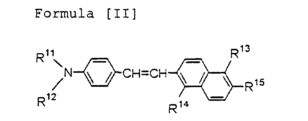 R11 and R12 may be the same or different and each independently represents a naphthyl group represented by the following formula (2):wherein R16, R17, R18, R19, R20, R21 and R22 may be the same or different, at least one of R16 to R22 represents a hydrogen atom, a saturated or unsaturated hydrocarbon group having at least one carbon atom, a saturated or unsaturated hydrocarbyloxy group having at least one carbon atom, a saturated or unsaturated hydrocarbylamino group having at least one carbon atom, a trifluoromethyl group, a cyano group or a halogen atom, and the remaining one or ones of R16 to R22, if any, are each a hydrogen atom, a saturated or unsaturated hydrocarbon group having at least one carbon atom, a saturated or unsaturated hydrocarbyloxy group having at least one carbon atom, a saturated or unsaturated hydrocarbylamino group having at least one carbon atom, a trifluoromethyl group, a cyano group or a halogen atom,
 R13 and R14 may be the same or different, one of R13 and R14 represents a hydrogen atom, a cyano group, a nitro group, a trifluoromethyl group or a halogen atom, and the remaining one represents a hydrogen atom, a cyano group, a nitro group, a trifluoromethyl group or a halogen atom, andR15 represents a substituted or unsubstituted, saturated or unsaturated alkyl group, a substituted or unsubstituted, alicyclic hydrocarbon group, a substituted or unsubstituted aryl group, a substituted or unsubstituted alkoxyl group, a substituted or unsubstituted, alicyclic hydrocarbyloxy group, or a substituted or unsubstituted, aromatic hydrocarbyloxy group.wherein:
 R23 is a phenyl group represented by the following formula (3):wherein R28 , R29, R30, R31 and R32 may be the same or different, at least one of R28 to R32 represents a hydrogen atom, a saturated or unsaturated hydrocarbon group having at least one carbon atom with a proviso that, when at least two adjacent ones of R28 to R32 each represents a saturated or unsaturated hydrocarbon group having at least one carbon atom, at least said two adjacent ones of R28 to R32 may be fused together to form a ring, a hydrocarbyloxy group having at least one carbon atom, a hydrocarbylamino group having at least one carbon atom, a trifluoromethyl group, a cyano group or a halogen atom, and the remaining one or ones of R29 to R32, if any, are each a hydrogen atom, a saturated or unsaturated hydrocarbon group having at least one carbon atom with a proviso that, when at least two adjacent ones of R28 to R32 each represents a saturated or unsaturated hydrocarbon group having at least one carbon atom, at least said two adjacent ones of R28 to R32 may be fused together to form a ring, a saturated or unsaturated hydrocarbyloxy group having at least one carbon atom, a saturated or unsaturated hydrocarbylamino group having at least one carbon atom, a trifluoromethyl group, a cyano group or a halogen atom,
 R24 represents a naphthyl group represented by the following formula (4):wherein R33, R34, R35 , R36, R37, R38 and R39 may be the same or different, at least one of R33 to R39 represents a hydrogen atom, a saturated or unsaturated hydrocarbon group having at least one carbon atom, a saturated or unsaturated hydrocarbyloxy group having at least one carbon atom, a saturated or unsaturated hydrocarbylamino group having at least one carbon atom, a trifluoromethyl group, a cyano group or a halogen atom, and the remaining one or ones of R33 to R39, if any, are each a hydrogen atom, a saturated or unsaturated hydrocarbon group having at least one carbon atom, a saturated or unsaturated hydrocarbyloxy group having at least one carbon atom, a saturated or unsaturated hydrocarbylamino group having at least one carbon atom, a trifluoromethyl group, a cyano group or a halogen atom,
 R25 and R26 may be the same or different, one of R25 and R26 represents a hydrogen atom, a cyano group, a nitro group, a trifluoromethyl group or a halogen atom, and the remaining one represents a hydrogen atom, a cyano group, a nitro group, a trifluoromethyl group or a halogen atom, andR27 represents a hydrogen atom, a substituted or unsubstituted, saturated or unsaturated alkyl group, a substituted or unsubstituted, alicyclic hydrocarbon group, a substituted or unsubstituted aryl group, a substituted or unsubstituted alkoxyl group, a substituted or unsubstituted, alicyclic hydrocarbyloxy group, or a substituted or unsubstituted, aromatic hydrocarbyloxy group.
 - The aminostyrylnaphthalene compound according to claim 8, which is represented by the formula (5), (6), (7), (8), (9), (10), (11), (12), (13), (14), (15), (16) or (17) as defined in claim 6.
- The process for the production of an aminostyrylnaphthalene compound represented by the formula [A] as defined in claim 7, which comprises subjecting a 4-aminobenzaldehyde represented by the following formula [B] and at least one of a phosphonate ester represented by the following formula [C] and a phosphonium represented by the following formula [D] to condensation:wherein Ra and Rb have the same meanings as defined above.

 Wherein Rj represents a hydrocarbon group, Rc, Rd, Re, Rf, Rg, Rh and Ri have the same meanings as defined above, and X represents a halogen atom.
- The process for the production of an aminostyrylnaphthalene compound represented by the formula [I], [II] or [III] as defined in claim 8, which comprises subjecting a 4-(N,N-diarylamino)benzaldehyde represented by the following formula [IV] and at least one of a phosphonate ester represented by the following formula [V] and a phosphonium represented by the following formula [VI] to condensation:wherein R71 and R72 each independently represents an aryl group corresponding to R1, R2, R11, R12, R23 or R24 as defined above.

 wherein R73 represents a hydrocarbon group, R74 and R75 each independently represents a group corresponding to R3, R4, R13, R14, R25 or R26 as defined above, R76 represents a group corresponding to R5, R15 or R27 as defined above, and X represents a halogen atom.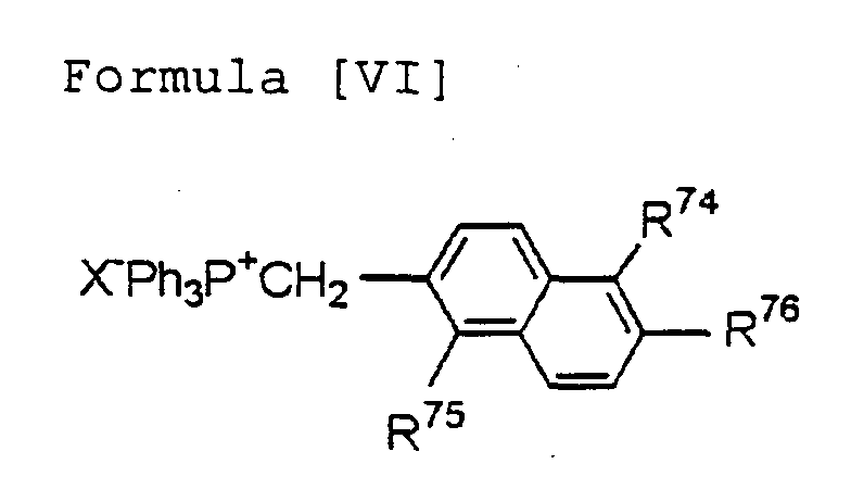
- The process according to claim 10, wherein said condensation is conducted by the Wittig-Horner reaction, at least one of said phosphonate ester and said phosphonium is treated with a base in a solvent to form carbanions, and said carbanions and said 4-(N,N-diarylamino)benzaldehyde are subjected to condensation.
- The process according to claim 10, wherein said condensation is conducted by the Wittig reaction, at least one of said phosphonate ester and said phosphonium is treated with a base in a solvent to form carbanions, and said carbanions and said 4-(N,N-diarylamino)benzaldehyde are subjected to condensation.
- The process according to claim 11, wherein an aminostyrylnaphthalene compound represented by the formula (5), (6), (7), (8), (9), (10), (11), (12), (13), (14), (15), (16) or (17) as defined in claim 6 is obtained.
- The phosphonate ester or phosphonium represented by the following formula [C] or [D] as defined in claim 10:
 wherein Rj represents a hydrocarbon group, Rc, Rd, Re, Rf, Rg, Rh and Ri have the same meanings as defined above, and X represents a halogen atom.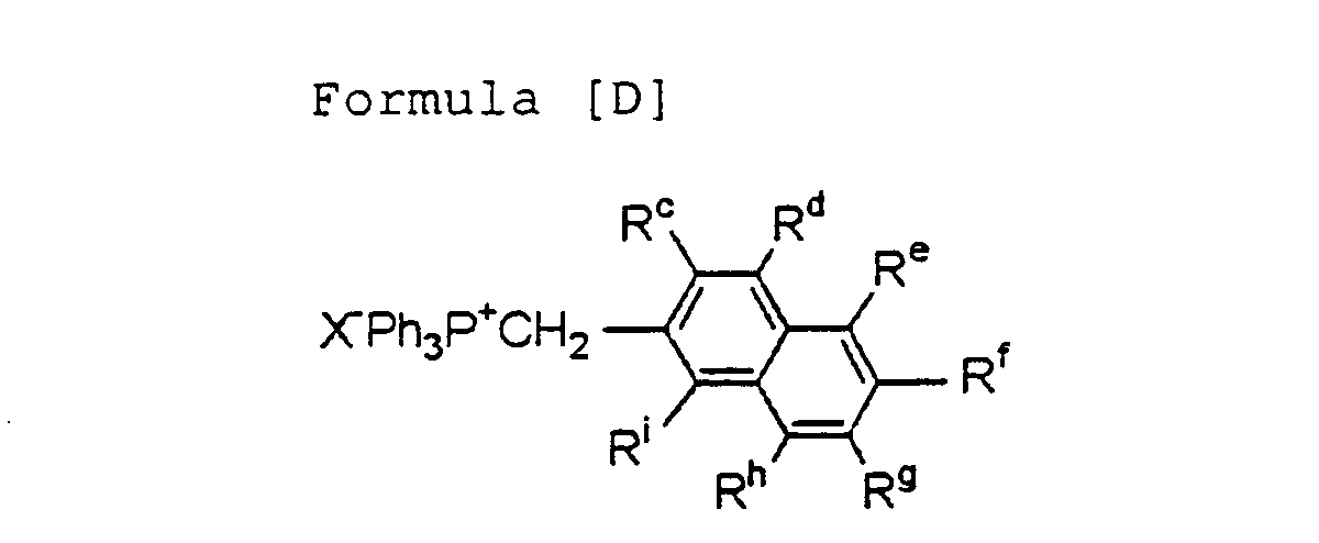
- The phosphonate ester or phosphonium as described in claim 11, which is represented by the following formula [V] or [VI]:
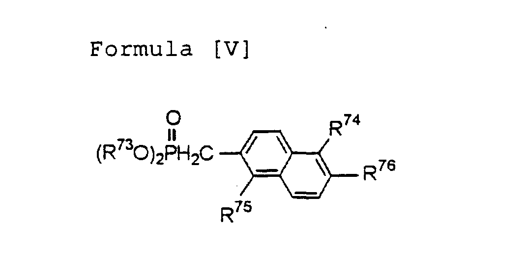 wherein R73 represents a hydrocarbon group, R74 and R75 each independently represents a group corresponding to R3, R4, R13, R14, R25 or R26, R76 represents a group corresponding to R5, R15 or R27, and X represents a halogen atom.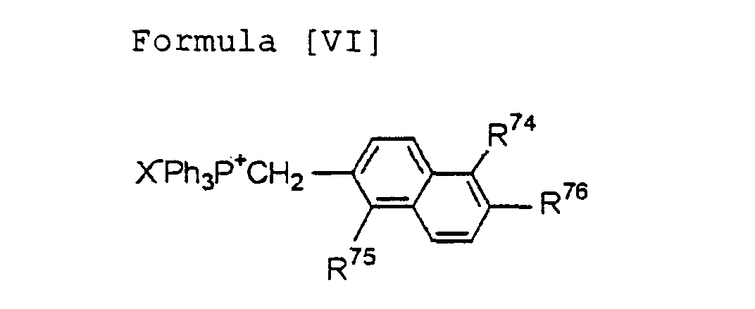
- The phosphonate ester according to claim 16, wherein R73 represents a saturated hydrocarbon group having 1 to 4 carbon atoms.
- The phosphonate ester or phosphonium according to claim 16, which is represented by the following formula (18) or (19):
 wherein R73 , R76 and X have the same meanings as defined above.
- The process for the production of a phosphonate ester or phosphonium represented by the formula [C] or [D] as defined in claim 15, which comprises reacting a halogenated aryl compound represented by the following formula [E] with a trialkyl phosphite represented by the following formula [F] or triphenylphosphine (PPh3):
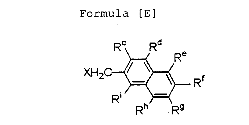
P(ORi)3 - The process for the production of a phosphonate ester or phosphonium represented by the formula [V] or [VI] as defined in claim 16, which comprises reacting a halogenated aryl compound represented by the following formula [VII] with a trialkyl phosphite represented by the following formula [VIII] or triphenylphosphine (PPh3):

P (OR73)3 - The process according to claim 20, wherein R73 represents a saturated hydrocarbon group having 1 to 4 carbon atoms.
- The process according to claim 20, wherein a phosphonate ester or phosphonium represented by the formula (18) or (19) as defined in claim 18 is obtained.
- A halogenated aryl compound represented by the following formula [E]:wherein:
 Rc, Rd, Re, Rg, Rh and Ri may be the same or different, at least one of Rc, Rd, Re, Rg, Rh and Ri independently represents a hydrogen atom, a cyano group, a nitro group, a trifluoromethyl group or a halogen atom, and the remaining one or ones of Rc, Rd, Re, Rg, Rh and Ri, if any, are each a hydrogen atom, a cyano group, a nitro group, a trifluoromethyl group or a halogen atom, andRf represents a substituted or unsubstituted, saturated or unsaturated alkyl group, a substituted or unsubstituted alicyclic hydrocarbon group, a substituted or unsubstituted aryl group, a substituted or unsubstituted alkoxyl group, a substituted or unsubstituted alicyclic hydrocarbyloxy group or a substituted or unsubstituted aromatic hydrocarbyloxy group.
 - A halogenated aryl compound according to claim 23, which is represented by the following formula [VII]:wherein R74 and R75 may be the same or different, one of R74 and R75 represents a hydrogen atom, a cyano group, a nitro group, a trifluoromethyl group or a halogen atom, and the remaining one represents a hydrogen atom, a cyano group, a nitro group, a trifluoromethyl group or a halogen atom; R76 represents a substituted or unsubstituted, saturated or unsaturated alkyl group, a substituted or unsubstituted, alicyclic hydrocarbon group, a substituted or unsubstituted aryl group, a substituted or unsubstituted alkoxyl group, a substituted or unsubstituted, alicyclic hydrocarbyloxy group, or a substituted or unsubstituted, aromatic hydrocarbyloxy group; and X represents a halogen atom.
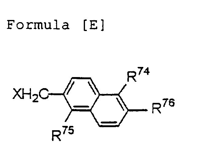
- A process for the production of a halogenated aryl compound represented by the formula [VII] as defined in claim 23, which comprises reacting a naphthalene compound represented by the following formula [G] with an N-halogenated succinimide represented by the following formula [H]:wherein Rc, Rd, Re, Rf , Rg, Rh and Ri have the same meanings as defined above.
 wherein X represents a halogen atom.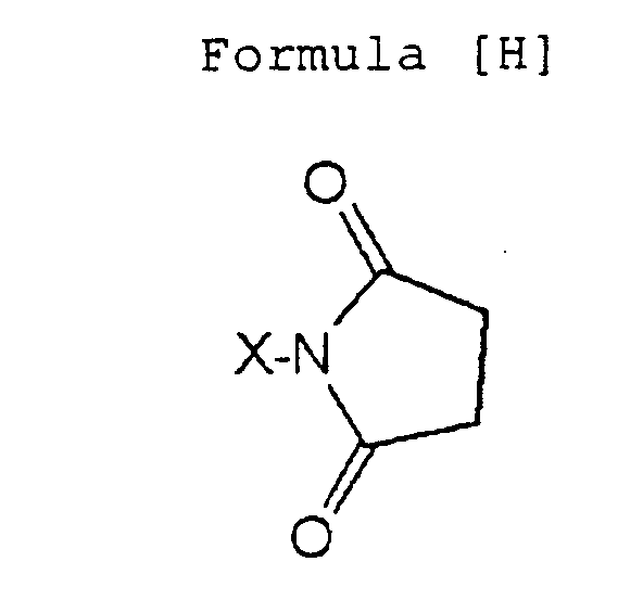
- The process according to claim 25, wherein a naphthalene compound represented by the following formula [IX] is used as said naphthalene compound to obtain a halogenated naphthalene compound represented by the formula [VII] as defined in claim 24.wherein R74 , R75 and R76 have the same meanings as defined above.

Applications Claiming Priority (4)
| Application Number | Priority Date | Filing Date | Title |
|---|---|---|---|
| JP2003079768 | 2003-03-24 | ||
| JP2003079768 | 2003-03-24 | ||
| JP2004033056 | 2004-02-10 | ||
| JP2004033056A JP4001118B2 (en) | 2003-03-24 | 2004-02-10 | Organic electroluminescent device and amino monostyryl naphthalene compound |
Publications (2)
| Publication Number | Publication Date |
|---|---|
| EP1473349A2 true EP1473349A2 (en) | 2004-11-03 |
| EP1473349A3 EP1473349A3 (en) | 2007-07-18 |
Family
ID=32993013
Family Applications (1)
| Application Number | Title | Priority Date | Filing Date |
|---|---|---|---|
| EP04007087A Withdrawn EP1473349A3 (en) | 2003-03-24 | 2004-03-24 | Organic electroluminescent devices, aminostyrylnaphthalene compounds and synthesis intermediates thereof, and production processes of the same |
Country Status (6)
| Country | Link |
|---|---|
| US (2) | US7402344B2 (en) |
| EP (1) | EP1473349A3 (en) |
| JP (1) | JP4001118B2 (en) |
| KR (1) | KR101055120B1 (en) |
| CN (1) | CN1533220B (en) |
| TW (1) | TWI326702B (en) |
Cited By (1)
| Publication number | Priority date | Publication date | Assignee | Title |
|---|---|---|---|---|
| WO2006046186A1 (en) * | 2004-10-28 | 2006-05-04 | Koninklijke Philips Electronics N.V. | Light-emitting diode with luminescent charge transport layer |
Families Citing this family (9)
| Publication number | Priority date | Publication date | Assignee | Title |
|---|---|---|---|---|
| US7837742B2 (en) | 2003-05-19 | 2010-11-23 | The Procter & Gamble Company | Cosmetic compositions comprising a polymer and a colorant |
| US7260171B1 (en) * | 2004-10-25 | 2007-08-21 | General Electric Company | Apparatus for acquisition of CT data with penumbra attenuation calibration |
| EP1937616B1 (en) | 2005-10-21 | 2014-12-17 | LG Chem, Ltd. | New binaphthalene derivatives, preparation method thereof and organic electronic device using the same |
| WO2007145976A2 (en) * | 2006-06-05 | 2007-12-21 | E. I. Du Pont De Nemours And Company | Process for making an organic light-emitting diode |
| JP4623166B2 (en) | 2008-08-25 | 2011-02-02 | ソニー株式会社 | Labeled compound and detection method using the same |
| KR101973207B1 (en) * | 2011-06-23 | 2019-04-29 | 삼성디스플레이 주식회사 | Anode including metal oxides and an organic light emitting device having the anode |
| KR101954980B1 (en) * | 2011-11-03 | 2019-05-31 | 삼성디스플레이 주식회사 | Heterocyclic compound and organic light-emitting diode comprising the same |
| KR101821256B1 (en) * | 2011-11-03 | 2018-01-24 | 삼성디스플레이 주식회사 | Heterocyclic compound and organic light-emitting diode comprising the same |
| CN103715368A (en) | 2013-12-27 | 2014-04-09 | 京东方科技集团股份有限公司 | Light emitting device, manufacturing method thereof and display device |
Family Cites Families (62)
| Publication number | Priority date | Publication date | Assignee | Title |
|---|---|---|---|---|
| US4107444A (en) | 1976-12-16 | 1978-08-15 | E. I. Du Pont De Nemours And Company | Thermally stable, rigid, aliphatic diols |
| US5004744A (en) | 1988-12-13 | 1991-04-02 | Bayer Aktiengesellschaft | Pyridazinones as pesticides |
| JP2897138B2 (en) | 1989-06-30 | 1999-05-31 | 株式会社リコー | EL device |
| JPH03269995A (en) * | 1990-03-16 | 1991-12-02 | Ricoh Co Ltd | Method for manufacturing electroluminescent device |
| JPH05194943A (en) | 1991-08-05 | 1993-08-03 | Idemitsu Kosan Co Ltd | Organic electroluminescent device |
| JPH0541285A (en) * | 1991-08-07 | 1993-02-19 | Ricoh Co Ltd | Electroluminescence element |
| JPH05105645A (en) | 1991-10-16 | 1993-04-27 | Mita Ind Co Ltd | Stilbene derivative and electrophotographic sensitive material containing the same |
| JPH05320632A (en) | 1992-05-20 | 1993-12-03 | Konica Corp | Organic electroluminescent element |
| JP3163589B2 (en) | 1992-09-21 | 2001-05-08 | 出光興産株式会社 | Organic electroluminescence device |
| JP3366401B2 (en) | 1992-11-20 | 2003-01-14 | 出光興産株式会社 | White organic electroluminescence device |
| US5399588A (en) | 1993-12-14 | 1995-03-21 | American Home Products Corporation | Naphthalenylmethyl cycloalkenone acetic acids and analogs thereof useful as aldose reductase inhibitors |
| CN1047387C (en) * | 1995-05-09 | 1999-12-15 | 中国科学院上海有机化学研究所 | Hapten compound, synthesis method and use thereof |
| JP3564859B2 (en) | 1996-04-01 | 2004-09-15 | 東洋インキ製造株式会社 | Organic electroluminescent device material and organic electroluminescent device using the same |
| JPH10245549A (en) | 1997-03-06 | 1998-09-14 | Minolta Co Ltd | Electroluminescent element |
| JP3890686B2 (en) | 1997-07-22 | 2007-03-07 | 東洋インキ製造株式会社 | Organic electroluminescence device |
| JP3864516B2 (en) | 1997-09-29 | 2007-01-10 | 東洋インキ製造株式会社 | Organic electroluminescent device material and organic electroluminescent device using the same |
| JP3852517B2 (en) | 1998-05-18 | 2006-11-29 | ソニー株式会社 | Organic electroluminescence device |
| JP3852518B2 (en) | 1998-05-18 | 2006-11-29 | ソニー株式会社 | Organic electroluminescence device |
| JPH11335307A (en) | 1998-05-26 | 1999-12-07 | Dainippon Ink & Chem Inc | Dialkenyl naphthalene derivative |
| JP3555736B2 (en) | 1998-06-26 | 2004-08-18 | ソニー株式会社 | Organic electroluminescent device |
| JP2000012225A (en) | 1998-06-26 | 2000-01-14 | Sony Corp | Organic electroluminescent device |
| JP2000012228A (en) | 1998-06-26 | 2000-01-14 | Sony Corp | Organic electroluminescent device |
| JP3820752B2 (en) | 1998-06-26 | 2006-09-13 | ソニー株式会社 | Organic electroluminescence device |
| FR2784528A1 (en) | 1998-10-13 | 2000-04-14 | Koninkl Philips Electronics Nv | METHOD OF CONSTRUCTING A SET OF CONSTELLATIONS TO BE USED FOR TRANSMITTING DATA BETWEEN A TRANSMITTER AND A RECEIVER |
| JP3646012B2 (en) | 1998-10-29 | 2005-05-11 | 京セラミタ株式会社 | Electrophotographic photoreceptor |
| JP4411708B2 (en) | 1998-12-07 | 2010-02-10 | ソニー株式会社 | Bis (aminostyryl) benzene compound |
| JP2000173773A (en) * | 1998-12-09 | 2000-06-23 | Sony Corp | Organic electroluminescent device |
| JP2000214610A (en) | 1999-01-26 | 2000-08-04 | Kyocera Mita Corp | Single layer type electrophotographic photoreceptor |
| JP2001037884A (en) | 1999-07-28 | 2001-02-13 | Kawasumi Lab Inc | Stent and method for manufacturing stent |
| TW480896B (en) | 1999-07-30 | 2002-03-21 | Sony Corp | Organic electroluminescent device |
| TW463520B (en) | 1999-07-30 | 2001-11-11 | Sony Corp | Organic electroluminescent device |
| JP4482964B2 (en) | 1999-08-16 | 2010-06-16 | 保土谷化学工業株式会社 | Electrophotographic photoreceptor |
| JP4164717B2 (en) | 1999-10-06 | 2008-10-15 | ソニー株式会社 | Bis (aminostyryl) anthracene compound, synthetic intermediate thereof, and production method thereof |
| JP4164718B2 (en) | 1999-10-06 | 2008-10-15 | ソニー株式会社 | Bis (aminostyryl) naphthalene compound and synthetic intermediate thereof, production method thereof, and organic electroluminescent device |
| US6492557B1 (en) * | 1999-10-06 | 2002-12-10 | Sony Corporation | Bis (aminostyryl) naphthalene compound, synthesis intermediate thereof, and process for production thereof |
| JP2001131174A (en) | 1999-11-02 | 2001-05-15 | Sony Corp | Vasophenanthroline compound and method for producing the same |
| JP3661540B2 (en) | 2000-01-25 | 2005-06-15 | 日立電線株式会社 | Flat heat pipe |
| JP3688207B2 (en) | 2000-02-18 | 2005-08-24 | 三星エスディアイ株式会社 | Organic EL device and organic EL display |
| US6689493B2 (en) | 2000-02-18 | 2004-02-10 | Nec Corporation | Organic electroluminescent element and organic electroluminescent display |
| JP2001288377A (en) | 2000-04-06 | 2001-10-16 | Sony Corp | Aminostyrylanthracene compounds, synthetic intermediates thereof, and methods for producing them |
| JP2001291591A (en) * | 2000-04-07 | 2001-10-19 | Sony Corp | Organic electroluminescent element and light emitting device |
| JP2001305754A (en) | 2000-04-18 | 2001-11-02 | Kyocera Mita Corp | Monolayer type electrophotographic photoreceptor |
| JP2001307884A (en) | 2000-04-26 | 2001-11-02 | Toray Ind Inc | Light emitting element |
| JP2002031901A (en) | 2000-05-12 | 2002-01-31 | Kyocera Mita Corp | Monolayer electrophotographic photoreceptor |
| JP2001337469A (en) | 2000-05-25 | 2001-12-07 | Kyocera Mita Corp | Single-layer type electrophotographic photoreceptor |
| JP2001337649A (en) | 2000-05-29 | 2001-12-07 | Mitsubishi Electric Corp | Plasma display device |
| EP1297021B1 (en) | 2000-06-15 | 2009-03-18 | 3M Innovative Properties Company | Multiphoton photosensitization system |
| JP2002022672A (en) | 2000-07-05 | 2002-01-23 | Toshiba Corp | Metal oxide or hydroxide pipe inner wall adhesion amount measuring apparatus, adhesion state evaluation method, and adhesion state prediction method |
| JP2002040676A (en) | 2000-07-24 | 2002-02-06 | Kyocera Mita Corp | Electrophotographic photoreceptor using specified polyester resin and charge transfer agent |
| JP2002040677A (en) | 2000-07-26 | 2002-02-06 | Kyocera Mita Corp | Electrophotographic photoreceptor used for device for image formation by wet development method |
| JP3616560B2 (en) | 2000-08-31 | 2005-02-02 | 京セラミタ株式会社 | Single layer type electrophotographic photoreceptor |
| DE60132141T2 (en) | 2000-08-31 | 2008-12-18 | Kyocera Mita Corp. | Single-layer type electrophotographic material |
| JP3583705B2 (en) | 2000-09-26 | 2004-11-04 | 京セラミタ株式会社 | Electrophotographic photoreceptor |
| JP3583707B2 (en) | 2000-10-11 | 2004-11-04 | 京セラミタ株式会社 | Electrophotographic photoreceptor used for wet development type image forming apparatus |
| JP2002131943A (en) | 2000-10-26 | 2002-05-09 | Kyocera Mita Corp | Monolayer type electrophotographic photoreceptor used for image forming device by wet developing method |
| JP2002134276A (en) | 2000-10-30 | 2002-05-10 | Sony Corp | Organic electroluminescent device |
| US6461779B1 (en) | 2000-11-14 | 2002-10-08 | Kyocera Mita Corporation | Single-layer type electrophotosensitive material |
| JP2002208488A (en) | 2001-01-12 | 2002-07-26 | Sony Corp | Organic electroluminescent device |
| JP4158078B2 (en) | 2001-01-30 | 2008-10-01 | ソニー株式会社 | Aminostyrylphenanthrene compounds and synthetic intermediates thereof |
| JP2002246175A (en) * | 2001-02-16 | 2002-08-30 | Sony Corp | Method and apparatus for forming organic material thin film, and method for manufacturing organic electroluminescent element |
| JP2004006066A (en) * | 2002-04-15 | 2004-01-08 | Sony Corp | Organic electroluminescent element and light emitting device |
| JP4161262B2 (en) * | 2002-06-26 | 2008-10-08 | ソニー株式会社 | ORGANIC ELECTROLUMINESCENT ELEMENT AND LIGHT EMITTING OR DISPLAY DEVICE USING THE SAME |
-
2004
- 2004-02-10 JP JP2004033056A patent/JP4001118B2/en not_active Expired - Fee Related
- 2004-03-24 CN CN2004100326500A patent/CN1533220B/en not_active Expired - Fee Related
- 2004-03-24 US US10/807,984 patent/US7402344B2/en not_active Expired - Lifetime
- 2004-03-24 TW TW093107940A patent/TWI326702B/en not_active IP Right Cessation
- 2004-03-24 KR KR1020040020020A patent/KR101055120B1/en not_active Expired - Fee Related
- 2004-03-24 EP EP04007087A patent/EP1473349A3/en not_active Withdrawn
-
2007
- 2007-06-20 US US11/765,560 patent/US7524991B2/en not_active Expired - Fee Related
Cited By (1)
| Publication number | Priority date | Publication date | Assignee | Title |
|---|---|---|---|---|
| WO2006046186A1 (en) * | 2004-10-28 | 2006-05-04 | Koninklijke Philips Electronics N.V. | Light-emitting diode with luminescent charge transport layer |
Also Published As
| Publication number | Publication date |
|---|---|
| US7402344B2 (en) | 2008-07-22 |
| TW200426202A (en) | 2004-12-01 |
| US20040265627A1 (en) | 2004-12-30 |
| CN1533220B (en) | 2013-05-15 |
| KR20040084775A (en) | 2004-10-06 |
| US20080051607A1 (en) | 2008-02-28 |
| CN1533220A (en) | 2004-09-29 |
| JP4001118B2 (en) | 2007-10-31 |
| KR101055120B1 (en) | 2011-08-08 |
| EP1473349A3 (en) | 2007-07-18 |
| JP2004307472A (en) | 2004-11-04 |
| US7524991B2 (en) | 2009-04-28 |
| TWI326702B (en) | 2010-07-01 |
Similar Documents
| Publication | Publication Date | Title |
|---|---|---|
| JP3228502B2 (en) | Organic electroluminescence device | |
| JP2003142269A (en) | Organic el display | |
| JP2004095221A (en) | Light emitting element | |
| US7524991B2 (en) | Organic electroluminescent devices, aminostyrylnaphthalene compounds and synthesis intermediates thereof, and production processes of the same | |
| US7087310B2 (en) | Bis (aminostyryl) naphthalene compound, synthesis intermediate thereof, and process for production thereof | |
| US6906217B2 (en) | Aminostyrylanthracene compound, synthetic intermediate thereof, and process for production thereof | |
| JP4164717B2 (en) | Bis (aminostyryl) anthracene compound, synthetic intermediate thereof, and production method thereof | |
| JP4158078B2 (en) | Aminostyrylphenanthrene compounds and synthetic intermediates thereof | |
| JP4792687B2 (en) | Charge transport material, light-emitting material containing diazapentacene derivative, and organic electroluminescent device using the same | |
| US10211410B2 (en) | Organic compound and electronic device using same | |
| US10217947B2 (en) | Organic compound and electronic device using same | |
| JP4329437B2 (en) | Bis (aminostyryl) phenanthrene compound, synthetic intermediate thereof, and organic electroluminescent device | |
| JP3874134B2 (en) | Organic electroluminescent device and tetraamine derivative | |
| KR100446466B1 (en) | Organic luminescent compound, and organic electroluminescence device using the same | |
| KR100813676B1 (en) | New electron injection layer material and organic light emitting device comprising the same | |
| KR100754474B1 (en) | Anthracene-based organic light emitting compound and organic light emitting diode comprising same | |
| JP2000268963A (en) | Organic EL device | |
| JP2007182401A (en) | Novel aromatic tertiary amines and their use | |
| US7022868B2 (en) | Aminostyrylanthracene compound, synthetic intermediate thereof, and process for production thereof | |
| US20050258743A1 (en) | Aminostyrylanthracene compound, synthetic intermediate thereof, and process for production thereof | |
| JP2009040792A (en) | Bis (aminostyryl) benzene compound | |
| WO2007064009A1 (en) | Light emitting element, light emitting device and electronic device | |
| JP2001131128A (en) | Bis (aminostyryl) stilbene-based compounds and synthetic intermediates thereof, methods for their production, and organic electroluminescent devices |
Legal Events
| Date | Code | Title | Description |
|---|---|---|---|
| PUAI | Public reference made under article 153(3) epc to a published international application that has entered the european phase |
Free format text: ORIGINAL CODE: 0009012 |
|
| AK | Designated contracting states |
Kind code of ref document: A2 Designated state(s): AT BE BG CH CY CZ DE DK EE ES FI FR GB GR HU IE IT LI LU MC NL PL PT RO SE SI SK TR |
|
| AX | Request for extension of the european patent |
Extension state: AL LT LV MK |
|
| RIC1 | Information provided on ipc code assigned before grant |
Ipc: H01L 51/00 20060101ALI20070313BHEP Ipc: C09K 11/06 20060101ALI20070313BHEP Ipc: H05B 33/14 20060101AFI20070313BHEP |
|
| PUAL | Search report despatched |
Free format text: ORIGINAL CODE: 0009013 |
|
| AK | Designated contracting states |
Kind code of ref document: A3 Designated state(s): AT BE BG CH CY CZ DE DK EE ES FI FR GB GR HU IE IT LI LU MC NL PL PT RO SE SI SK TR |
|
| AX | Request for extension of the european patent |
Extension state: AL LT LV MK |
|
| 17P | Request for examination filed |
Effective date: 20071219 |
|
| 17Q | First examination report despatched |
Effective date: 20080205 |
|
| AKX | Designation fees paid |
Designated state(s): DE FR GB |
|
| STAA | Information on the status of an ep patent application or granted ep patent |
Free format text: STATUS: THE APPLICATION IS DEEMED TO BE WITHDRAWN |
|
| 18D | Application deemed to be withdrawn |
Effective date: 20141001 |