EP1471166A2 - Layer with controlled grain size and morphology for enhanced wear resistance - Google Patents

Layer with controlled grain size and morphology for enhanced wear resistance Download PDF

Info

Publication number
EP1471166A2
EP1471166A2 EP04009403A EP04009403A EP1471166A2 EP 1471166 A2 EP1471166 A2 EP 1471166A2 EP 04009403 A EP04009403 A EP 04009403A EP 04009403 A EP04009403 A EP 04009403A EP 1471166 A2 EP1471166 A2 EP 1471166A2
Authority
EP
European Patent Office
Prior art keywords
layer
coating
mtcvd
hkl
coatings
Prior art date
Legal status (The legal status is an assumption and is not a legal conclusion. Google has not performed a legal analysis and makes no representation as to the accuracy of the status listed.)
Withdrawn
Application number
EP04009403A
Other languages
German (de)
French (fr)
Other versions
EP1471166A3 (en
Inventor
Sakari Ruppi
Current Assignee (The listed assignees may be inaccurate. Google has not performed a legal analysis and makes no representation or warranty as to the accuracy of the list.)
Seco Tools AB
Original Assignee
Seco Tools AB
Priority date (The priority date is an assumption and is not a legal conclusion. Google has not performed a legal analysis and makes no representation as to the accuracy of the date listed.)
Filing date
Publication date
Application filed by Seco Tools AB filed Critical Seco Tools AB
Publication of EP1471166A2 publication Critical patent/EP1471166A2/en
Publication of EP1471166A3 publication Critical patent/EP1471166A3/en
Withdrawn legal-status Critical Current

Links

Images

Classifications

    • CCHEMISTRY; METALLURGY
    • C23COATING METALLIC MATERIAL; COATING MATERIAL WITH METALLIC MATERIAL; CHEMICAL SURFACE TREATMENT; DIFFUSION TREATMENT OF METALLIC MATERIAL; COATING BY VACUUM EVAPORATION, BY SPUTTERING, BY ION IMPLANTATION OR BY CHEMICAL VAPOUR DEPOSITION, IN GENERAL; INHIBITING CORROSION OF METALLIC MATERIAL OR INCRUSTATION IN GENERAL
    • C23CCOATING METALLIC MATERIAL; COATING MATERIAL WITH METALLIC MATERIAL; SURFACE TREATMENT OF METALLIC MATERIAL BY DIFFUSION INTO THE SURFACE, BY CHEMICAL CONVERSION OR SUBSTITUTION; COATING BY VACUUM EVAPORATION, BY SPUTTERING, BY ION IMPLANTATION OR BY CHEMICAL VAPOUR DEPOSITION, IN GENERAL
    • C23C16/00Chemical coating by decomposition of gaseous compounds, without leaving reaction products of surface material in the coating, i.e. chemical vapour deposition [CVD] processes
    • C23C16/22Chemical coating by decomposition of gaseous compounds, without leaving reaction products of surface material in the coating, i.e. chemical vapour deposition [CVD] processes characterised by the deposition of inorganic material, other than metallic material
    • C23C16/30Deposition of compounds, mixtures or solid solutions, e.g. borides, carbides, nitrides
    • C23C16/36Carbonitrides
    • EFIXED CONSTRUCTIONS
    • E02HYDRAULIC ENGINEERING; FOUNDATIONS; SOIL SHIFTING
    • E02DFOUNDATIONS; EXCAVATIONS; EMBANKMENTS; UNDERGROUND OR UNDERWATER STRUCTURES
    • E02D29/00Independent underground or underwater structures; Retaining walls
    • E02D29/02Retaining or protecting walls
    • E02D29/0258Retaining or protecting walls characterised by constructional features
    • E02D29/0266Retaining or protecting walls characterised by constructional features made up of preformed elements
    • AHUMAN NECESSITIES
    • A01AGRICULTURE; FORESTRY; ANIMAL HUSBANDRY; HUNTING; TRAPPING; FISHING
    • A01GHORTICULTURE; CULTIVATION OF VEGETABLES, FLOWERS, RICE, FRUIT, VINES, HOPS OR SEAWEED; FORESTRY; WATERING
    • A01G9/00Cultivation in receptacles, forcing-frames or greenhouses; Edging for beds, lawn or the like
    • A01G9/02Receptacles, e.g. flower-pots or boxes; Glasses for cultivating flowers
    • A01G9/022Pots for vertical horticulture
    • A01G9/025Containers and elements for greening walls
    • CCHEMISTRY; METALLURGY
    • C23COATING METALLIC MATERIAL; COATING MATERIAL WITH METALLIC MATERIAL; CHEMICAL SURFACE TREATMENT; DIFFUSION TREATMENT OF METALLIC MATERIAL; COATING BY VACUUM EVAPORATION, BY SPUTTERING, BY ION IMPLANTATION OR BY CHEMICAL VAPOUR DEPOSITION, IN GENERAL; INHIBITING CORROSION OF METALLIC MATERIAL OR INCRUSTATION IN GENERAL
    • C23CCOATING METALLIC MATERIAL; COATING MATERIAL WITH METALLIC MATERIAL; SURFACE TREATMENT OF METALLIC MATERIAL BY DIFFUSION INTO THE SURFACE, BY CHEMICAL CONVERSION OR SUBSTITUTION; COATING BY VACUUM EVAPORATION, BY SPUTTERING, BY ION IMPLANTATION OR BY CHEMICAL VAPOUR DEPOSITION, IN GENERAL
    • C23C30/00Coating with metallic material characterised only by the composition of the metallic material, i.e. not characterised by the coating process
    • C23C30/005Coating with metallic material characterised only by the composition of the metallic material, i.e. not characterised by the coating process on hard metal substrates
    • EFIXED CONSTRUCTIONS
    • E02HYDRAULIC ENGINEERING; FOUNDATIONS; SOIL SHIFTING
    • E02DFOUNDATIONS; EXCAVATIONS; EMBANKMENTS; UNDERGROUND OR UNDERWATER STRUCTURES
    • E02D2600/00Miscellaneous
    • E02D2600/20Miscellaneous comprising details of connection between elements
    • EFIXED CONSTRUCTIONS
    • E02HYDRAULIC ENGINEERING; FOUNDATIONS; SOIL SHIFTING
    • E02DFOUNDATIONS; EXCAVATIONS; EMBANKMENTS; UNDERGROUND OR UNDERWATER STRUCTURES
    • E02D2600/00Miscellaneous
    • E02D2600/40Miscellaneous comprising stabilising elements
    • YGENERAL TAGGING OF NEW TECHNOLOGICAL DEVELOPMENTS; GENERAL TAGGING OF CROSS-SECTIONAL TECHNOLOGIES SPANNING OVER SEVERAL SECTIONS OF THE IPC; TECHNICAL SUBJECTS COVERED BY FORMER USPC CROSS-REFERENCE ART COLLECTIONS [XRACs] AND DIGESTS
    • Y02TECHNOLOGIES OR APPLICATIONS FOR MITIGATION OR ADAPTATION AGAINST CLIMATE CHANGE
    • Y02PCLIMATE CHANGE MITIGATION TECHNOLOGIES IN THE PRODUCTION OR PROCESSING OF GOODS
    • Y02P60/00Technologies relating to agriculture, livestock or agroalimentary industries
    • Y02P60/20Reduction of greenhouse gas [GHG] emissions in agriculture, e.g. CO2
    • YGENERAL TAGGING OF NEW TECHNOLOGICAL DEVELOPMENTS; GENERAL TAGGING OF CROSS-SECTIONAL TECHNOLOGIES SPANNING OVER SEVERAL SECTIONS OF THE IPC; TECHNICAL SUBJECTS COVERED BY FORMER USPC CROSS-REFERENCE ART COLLECTIONS [XRACs] AND DIGESTS
    • Y10TECHNICAL SUBJECTS COVERED BY FORMER USPC
    • Y10TTECHNICAL SUBJECTS COVERED BY FORMER US CLASSIFICATION
    • Y10T428/00Stock material or miscellaneous articles
    • Y10T428/25Web or sheet containing structurally defined element or component and including a second component containing structurally defined particles
    • Y10T428/252Glass or ceramic [i.e., fired or glazed clay, cement, etc.] [porcelain, quartz, etc.]
    • YGENERAL TAGGING OF NEW TECHNOLOGICAL DEVELOPMENTS; GENERAL TAGGING OF CROSS-SECTIONAL TECHNOLOGIES SPANNING OVER SEVERAL SECTIONS OF THE IPC; TECHNICAL SUBJECTS COVERED BY FORMER USPC CROSS-REFERENCE ART COLLECTIONS [XRACs] AND DIGESTS
    • Y10TECHNICAL SUBJECTS COVERED BY FORMER USPC
    • Y10TTECHNICAL SUBJECTS COVERED BY FORMER US CLASSIFICATION
    • Y10T428/00Stock material or miscellaneous articles
    • Y10T428/26Web or sheet containing structurally defined element or component, the element or component having a specified physical dimension
    • Y10T428/263Coating layer not in excess of 5 mils thick or equivalent
    • Y10T428/264Up to 3 mils
    • Y10T428/2651 mil or less
    • YGENERAL TAGGING OF NEW TECHNOLOGICAL DEVELOPMENTS; GENERAL TAGGING OF CROSS-SECTIONAL TECHNOLOGIES SPANNING OVER SEVERAL SECTIONS OF THE IPC; TECHNICAL SUBJECTS COVERED BY FORMER USPC CROSS-REFERENCE ART COLLECTIONS [XRACs] AND DIGESTS
    • Y10TECHNICAL SUBJECTS COVERED BY FORMER USPC
    • Y10TTECHNICAL SUBJECTS COVERED BY FORMER US CLASSIFICATION
    • Y10T428/00Stock material or miscellaneous articles
    • Y10T428/30Self-sustaining carbon mass or layer with impregnant or other layer

Definitions

  • the present invention relates to a cutting tool inserts consisting of a substrate at least partially coated with a coating consisting of one or more refractory layers of which at least one layer is a MTCVD-Ti(C,N)-layer composed of grains with grain size just above the nanograined region with columnar grain morphology.
  • a MTCVD-Ti(C,N)-layer composed of grains with grain size just above the nanograined region with columnar grain morphology.
  • Coated bodies used for metal cutting are well known.
  • the bodies are made of a cemented carbide, cermet or ceramic and the coatings are one or more of a Group VIB metal carbide, nitride, oxide or mixtures thereof.
  • cemented carbides coated with layers of TiC, Ti(C,N), Al 2 O 3 and TiN are widely used.
  • layer composition and thickness There are many variations in layer composition and thickness.
  • the layers are applied by various methods such as CVD (chemical vapour deposition), both conducted at normal temperatures of from about 900 to 1100 °C and MTCVD (medium temperature chemical vapour deposition) conducted at temperatures of from about 700 to 900°C, and PVD (physical vapour deposition).
  • CVD TiC coatings are usually composed of equiaxed grains with the grain size being form about 0.5 to 1.0 microns.
  • CVD TiN as well as MTCVD TiCN coatings are composed of columnar grains with the length of the grains approaching the coating layer thickness.
  • the morphology of CVD coatings can be slightly modified by process adjustments.
  • the MTCVD coatings are, however, very difficult to modify by conventional process adjustments.
  • MTCVD coatings are particularly characterized by the presence of large columnar grains with the length of the crystals approaching the thickness of the coating layer.
  • Ti(C,N) layers produced by using MTCVD are today almost exclusively used instead of CVD TiC or Ti(C,N).
  • H H° +C/ ⁇ d
  • the hardness of a polycrystalline material
  • the hardness of a single crystal
  • C a material constant (C>0)
  • d the grain size.
  • U.S. 6,472,060 discloses a method where relatively high amounts of CO, from about 5 to 10 %, preferably from about 7 to 9% of the total gaseous mixture, are used in MTCVD in order to obtain a grain size of the order of 25 nm or less, preferably 10 nm or less.
  • the CO-doped nanograined MTCVD coatings exhibited increased toughness, however, with reduced crater wear resistance as a consequence.
  • nanocrystalline coatings can be used as friction reducing/lubricating layers and should, as mentioned above, deposited on top of the existing coating structure.
  • the columnar structure is the preferred embodiment.
  • the grain size of MTCVD Ti(C,N) can be reduced, simultaneously maintaining the columnar structure. In this way the problems with grain boundary sliding at higher temperatures will be reduced.
  • the coating according to this invention consists of needle-like columnar crystals.
  • the fine-grained, columnar structure exhibits less grain boundary sliding than equiaxed coatings of the same grain size do at the same temperature and should be used in carbon steels or grey cast irons where wear resistance is important.
  • the ideal situation in the above indicated wear resistance demanding applications is to control the deposition process so that the Ti(C,N) layer is composed of fine needle-like (columnar) grains. It has been found possible to control CVD process and the grain size and shape by using texture- and structure-modifying agents (referred to as dopants in this application) in such degree that these structures can be produced industrially.
  • a coated body having as a MTCVD layer of Ti(C,N) as a part of a multicoating layer or as a single layer the said layer having an columnar grain morphology with the grain width of 30-300 nm, preferably from 50 to 200 nm and most preferably from 50 to 100 nm.
  • a method of forming a coated body of MTCVD Ti(C,N) comprising contacting a body with a gas containing titanium halide, nitrogen and carbon compound and a reducing agent.
  • controlled dopant addition of CO, ZrCl 4 , HfCl 4 and/or AlCl 3 can be used to form Ti(C,N) coatings in the specified range of grain size and shape.
  • the above mentioned coatings can be used in combination of other CVD materials such as alumina to enhance the performance and wear resistance of the prior-art products.
  • controlled reduction of the grain size of the MTCVD layers simultaneously maintaining the columnar grain morphology enhances the wear resistance by more than 100% over the prior-art MTCVD coatings in carbon steels and cast iron. Especially important is that crater wear resistance is enhanced with maintained toughness.
  • the coatings according to this invention increase the cutting performance at higher cutting speeds and can be combined with alumina layers to tailor-made a tool for extreme high-speed applications.
  • the process can be performed in a controlled way by using modem CVD reactors from the typical MTCVD temperatures of the order of 800-900 °C up to 1000 °C.
  • a cutting tool insert consisting of a substrate at least partially coated with a coating with a total thickness of 10-40 ⁇ m, preferably 15-25 ⁇ m consisting of one or more refractory layers of which at least one layer is a MTCVD-Ti(C,N)-layer with columnar grains with a thickness of 3 to 30 ⁇ m, preferably 5-20 ⁇ m.
  • the columnar grains should have a width from 30-300 nm, preferably 50 to 200 nm and most preferably 50 to 100 nm.
  • the L/W ratio (Length/Width) should be higher than 3, preferably higher than 5 and most preferably higher than 10.
  • This kind of coating is consequently composed of fine, needle-like grains and shows clearly enhanced wear resistance. Wear resistance of these coatings may exceed that of the prior art MTCVD Ti(C,N) coating deposited from the TiCl 4 -CH 3 CN-N 2 -H 2 system by up to several hundreds of percents.
  • the said layer can be applied onto an ⁇ -Al 2 O 3 , ⁇ -Al 2 O 3 or ⁇ -Al 2 O 3 layer which itself has been deposited on top the said layer.
  • the fine-grained, columnar morphology can be obtained by using extremely low and controlled levels of CO and/or ZrCl 4 or HfCl 4 doping. These dopants can be added simultaneously and preferably together with AlCl 3 .
  • the amount of CO should be from 0.1 to 1.0% and most preferably from 0.2 to 0.8%.
  • ZrCl 4 and HfCl 4 should be applied in the range of 0.1 to 0.5%, preferably from 0.2 to 0.3% and AlCl 3 should be applied in the range of 0.5 to 3.0%, preferably from 1.0 to 1.5%.
  • Very low amounts of CO 2 can be used. In this case we want to avoid equiaxed grain morphology and, thus, CO 2 should be used with extreme care.
  • CO 2 must be less than 0.1%, preferably from 0.01 to 0.08% of the total flow with a high CO/CO 2 ratio.
  • the CO/CO 2 ratio should be higher than 8, preferably higher than 10 and if possible about 15.
  • the deposition is performed at a temperature of from 700 to 1000°C, preferably 800-900°C.
  • Table 1 the effects of the additions of ZrCl 4 , HfCl 4 , AlCl 3 , CO or CO 2 dopants in the TiCl 4 -CH 3 CN-N 2 -H 2 system are depicted.
  • the coatings were deposited at 880 °C and at a total pressure of 70 mbar.
  • the grain size depends on the coating thickness.
  • the prior-art CVD coatings show large variation in grain size: in the near vicinity of the substrate the coating may be composed of sub-micron grains while on top of the coating the grain size may be of the order of several micrometers.
  • the present invention relates the cutting performance with the growth texture.
  • the growth texture can be described by texture coefficients (TC), which are determined as follows: where
  • the texture coefficient for all coatings according to this invention should be as follows:
  • the texture coefficient for 422 (TC(422)) should be higher than 5.0, preferably higher than 6 and most preferably higher than 7 or the texture coefficient for 331 (TC(331)) should be higher than 4, preferably higher than 5 and most preferably higher than 6.
  • line broadening of the 422 reflection should be less than 2.0 expressed as a relative value, the reference being non-doped prior-art Ti(C,N).
  • Line broadening is defined as B n /B 0 , where B 0 is the Full Width at Half Maximum (FWHM) of the reference reflection and B n is the Full Width at Half Maximum (FWHM) of the corresponding reflection of the coating according to this invention. Both are measured from K ⁇ 2 - stripped Gaussian profiles of the 422 reflection.
  • Line broadening is also a useful means to control that the produced layer has not been brought into the nanograined region manifested by strong line broadening.
  • the FWHM of either (422) or (331) diffraction peaks should be less than 1.5°, preferably less than 1.2° most preferably less than 1.0 °.
  • compositions of the obtained layers can be described by the following formula (Ti x Al y X z )(C u O w N v ), where x, u and v >0 and at least one of y, z and w >0.
  • the compositions of the layers according to this invention should be varied in the following limits: x is from 0.3 to 0.8, y is from 0.0 to 0.1, z is from 0.0 to 0.1, u is from 0.3 to 0.9, w is from 0.0 to 0.1 and y is from 0.3 to 0.6.
  • X can be selected from groups 4 to 6.
  • the useful elements are Zr, Hf, Nb, Ta or Mo even though Zr and Hf are used preferably.
  • the substrate comprises a hard material such as cemented carbide, cermets, ceramics, high speed steel or a superhard material such as cubic boron nitride (CBN) or diamond preferably cemented carbide or CBN.
  • CBN cubic boron nitride
  • the substrate is a cemented carbide with or without a binder phase enriched surface zone.
  • coatings 1, 2, 3, 4 and 5 were produced at a pressure of 70 mbar and at a temperature of 880°C according to the process data given in Table 2. Compared with the U.S. 6,472,060, considerably lower amounts of doping were used except coating 5, which was produced according to prior art U.S. 6,472,060.
  • a maximum amount of CO should be less than 1%, preferably from 0.1 to 0.8%. In this example 0.8% of CO was used (Coating 2).
  • Coating 3 was deposited at CO doping level of 2.5% to obtain equiaxed grain morphology.
  • Coating 4 was deposited using ZrCl 4 doping to obtain columnar morphology.
  • Coating 5 was deposited using 8% CO according to U.S. 6,472,060 to obtain a nanograined layer.
  • Coating 1 was deposited according to prior art without any dopant addition and is an example of a typical structure of a MTCVD coating.
  • Cemented carbide cutting inserts with a composition of 6.0% Co and balance WC (hardness about 1580 HV) were used as substrates in all Examples.
  • the following geometries were used in the cutting tests: SNUN120408 and CNMG120408-M3.
  • Example 1 The coatings from Example 1 were investigated using Transmission electron microscopy (TEM) and Scanning electron microscopy (SEM) in order to elucidate the effect of CO and ZrCl 4 doping on the grain size and morphology. It appeared clear even in SEM that the microstructure of the typical MTCVD Ti(C,N) coating being composed of large columnar crystals (Fig. 1) can be refined by CO doping. The obtained layer was composed of needle like crystals as shown in Fig. 2 at a CO doping level of 0.8%. Similar surface morphologies could be obtained either by ZrCl 4 or HfCl 4 doping alone or together with CO. The equiaxed grain morphology was obtained at CO doping level of 2.5%.
  • TEM Transmission electron microscopy
  • SEM Scanning electron microscopy
  • coatings 6, 7, 8, 9 and 10 were produced at a pressure of 70 mbar and at a temperature of 880°C according to the process data given in Table 4.
  • the coating thickness was 8 ⁇ m for all coatings.
  • CO 2 was not used in this particular example but could be applied with extreme care because coatings can in the presence of this precursor easily be brought into the nanograined region with equiaxed grain size.
  • the coatings were studied by using TEM together with EDS/WDS. The results are presented in Table 5. Surface morphology of Coating 9 is shown in Fig.3.
  • Coating 6 70 x 650 nm Needle-like Traces of Zr Coating 7 55 x 750 nm Needle-like 1.32 wt % Zr Coating 8 45 x 820 nm Needle-like 1.33 wt % Zr Coating 9 75 x 400 nm Needle-like 2.11 wt % Zr 0.91 wt % Al Coating 10 90 x 450
  • the coatings 1, 2, 3, 4 and 8 were studied using XRD.
  • the texture coefficients were determined according to the following.
  • Coatings 1, 2, 4 and 8 were studied by using XRD.
  • the grain refinement was slightly manifested as line broadening.
  • XRD demonstrated that the coatings according to this invention are not in the nanograined region, Table 7.
  • Grain Shape Coating 1 0.541 (B 0 ) 1.00
  • Large columnar Coating 2 0.849 (B n 2 ) 1,57 columnar Coating 4 0.860 (B n 4 ) 1.59 columnar Coating 8 0,924 (B n 8 ) 1.71 columnar
  • Typical X-ray diffraction patterns originating from Coating 2 (Example 1) and Coating 3 (Example 1) are shown in Figs 4 and 5, respectively.
  • Coating 2 (Fig. 4) is deposited according to this invention and is composed of needle-like grains with a strong 422-diffraction peak and Coating 3 (Fig. 5) is composed of small columnar grains. The differences are clear.
  • XRD easily can be used to show that the coating is composed of columnar grains and not of equiaxed grains or visa versa. Further, XRD can be used to verify that the grain size is not brought into the nanograined region.
  • Example 1 The coatings produced in Example 1 were tested in carbon steel under the following conditions: Work piece Cylindrical bar Material SS1672 Insert type SNUN120418 Cutting speed 250 and 400 m/min Feed 0.5 mm/rev Depth of cut 2.5 mm Remarks Dry turning
  • Results are shown in Table 9. All coatings composed of fine-grained columnar crystals outperformed the reference coating (Coating 1) composed of large columnar grains and also the coating composed of equiaxed grains (Coating 3). The coatings 7 and 8 with the highest L/W ratios were found to show the longest tool life.

Landscapes

  • Chemical & Material Sciences (AREA)
  • Engineering & Computer Science (AREA)
  • Chemical Kinetics & Catalysis (AREA)
  • Materials Engineering (AREA)
  • Mechanical Engineering (AREA)
  • Metallurgy (AREA)
  • Organic Chemistry (AREA)
  • Inorganic Chemistry (AREA)
  • General Chemical & Material Sciences (AREA)
  • Life Sciences & Earth Sciences (AREA)
  • Environmental Sciences (AREA)
  • Environmental & Geological Engineering (AREA)
  • General Life Sciences & Earth Sciences (AREA)
  • Mining & Mineral Resources (AREA)
  • Paleontology (AREA)
  • Civil Engineering (AREA)
  • General Engineering & Computer Science (AREA)
  • Structural Engineering (AREA)
  • Chemical Vapour Deposition (AREA)
  • Cutting Tools, Boring Holders, And Turrets (AREA)

Abstract

Deposition of medium temperature chemical vapor deposition titanium (carbon, nitrogen) layer involves addition of dopant to obtain a layer composed of columnar grains with width of 30-300, preferably 50-200 nm and with length:width ratio >= 3, preferably greater than 5.

Description

BACKGROUND OF THE INVENTION
The present invention relates to a cutting tool inserts consisting of a substrate at least partially coated with a coating consisting of one or more refractory layers of which at least one layer is a MTCVD-Ti(C,N)-layer composed of grains with grain size just above the nanograined region with columnar grain morphology. As a result the problem with grain boundary sliding at higher temperatures has been reduced and, consequently, wear resistance increased. The inserts are particularly useful in applications involving carbon steels or grey cast irons where wear resistance is important.
Coated bodies used for metal cutting are well known. Typically, the bodies are made of a cemented carbide, cermet or ceramic and the coatings are one or more of a Group VIB metal carbide, nitride, oxide or mixtures thereof. For example, cemented carbides coated with layers of TiC, Ti(C,N), Al2O3 and TiN are widely used. There are many variations in layer composition and thickness. The layers are applied by various methods such as CVD (chemical vapour deposition), both conducted at normal temperatures of from about 900 to 1100 °C and MTCVD (medium temperature chemical vapour deposition) conducted at temperatures of from about 700 to 900°C, and PVD (physical vapour deposition).
CVD TiC coatings are usually composed of equiaxed grains with the grain size being form about 0.5 to 1.0 microns. CVD TiN as well as MTCVD TiCN coatings are composed of columnar grains with the length of the grains approaching the coating layer thickness. The morphology of CVD coatings can be slightly modified by process adjustments. The MTCVD coatings are, however, very difficult to modify by conventional process adjustments. MTCVD coatings are particularly characterized by the presence of large columnar grains with the length of the crystals approaching the thickness of the coating layer. Ti(C,N) layers produced by using MTCVD are today almost exclusively used instead of CVD TiC or Ti(C,N).
It is well-known that the hardness of polycrystalline materials in general (including coating layers as well) obey the Hall-Petch equation: H=H° +C/√d where H is the hardness of a polycrystalline material, H° is the hardness of a single crystal, C is a material constant (C>0) and d is the grain size. As may be seen from this equation, the hardness of a material can be increased by decreasing the grain size.
This relation is, however, not necessarily correct for hard and brittle materials with limited plasticity. Furthermore, when dealing with nanograined hard materials with extremely fine grain sizes, the fraction of material in grain boundaries is increased and this effect has to be taken into consideration. Consequently, a reverse Hall-Petch dependence has been observed in many studies dealing with nanograined materials. Generally, it is assumed that the relationship is valid for grain sizes down to 20-50 nm. At these crystal sizes, mobility and multiplication of dislocations will be severely reduced. The properties of grain boundaries will start to dominate and grain boundary sliding has been suggested to be responsible for the reverse Hall-Petch dependence.
As clear from U.S. 6,472,060 the crater wear resistance is reduced when the grain size is decreased in to the nanograined region even though the room temperature hardness is increased. This is explained by increased amount of grain-boundary sliding. Consequently, when wear resistance is considered there is an optimum grain size region just above the nanograined region for the maximum performance. It is emphasised that the optimum grain shape (morphology) is not the same for all work piece materials and should consequently be controlled for different cutting conditions and work piece materials. In all applications, however, the grain size should be slightly above the nanograined region.
PRIOR ART
The use of different dopants such as a tetravalent titanium, hafnium and/or zirconium compound in the formation of an Al2O3 layer to promote the formation of a particular phase is shown in U.S. Reissue Patent 31,526. Also, the use of a dopant selected from the group consisting of sulphur, selenium, tellurium, phosphorous, arsenic, antimony, bismuth and mixtures thereof to increase the growth rate of Al2O3 applied by CVD as well as to promote even layers of the coating is disclosed in U.S. Patent 4,619,886. Dopants can also be applied to refine the grain size of MTCVD coatings. The use of CO doping to achieve nanograined MTCVD Ti(C,N) layers is disclosed in U.S. 6,472,060
U.S. 6,472,060 discloses a method where relatively high amounts of CO, from about 5 to 10 %, preferably from about 7 to 9% of the total gaseous mixture, are used in MTCVD in order to obtain a grain size of the order of 25 nm or less, preferably 10 nm or less. The CO-doped nanograined MTCVD coatings exhibited increased toughness, however, with reduced crater wear resistance as a consequence.
It has previously been shown (U.S. 6,472,060) that the grain size of MTCVD coatings can be decreased considerably and brought into the nanograined region. These nanocrystalline layers should preferably be applied as outermost layers. The nanocrystalline coatings are harder at room temperature but exhibit gram boundary sliding leading to plastic deformation at higher temperatures (at higher cutting speeds).
Due to the extremely fine grain size of these coatings, the surface smoothness is increased and friction coefficient is reduced. Consequently, nanocrystalline coatings can be used as friction reducing/lubricating layers and should, as mentioned above, deposited on top of the existing coating structure.
There is consequently still need to optimise and control the grain size of MTCVD coatings with respect to the material to be machined.
OBJECTS AND SUMMARY OF THE INVENTION
It is an object of this invention to avoid or alleviate the problems of the prior art by providing a coating layer having a controlled grain size, just above the nanograined region, and controlled morphology. In this case the columnar structure is the preferred embodiment.
According to this invention the grain size of MTCVD Ti(C,N) can be reduced, simultaneously maintaining the columnar structure. In this way the problems with grain boundary sliding at higher temperatures will be reduced. Thus, the coating according to this invention consists of needle-like columnar crystals.
The fine-grained, columnar structure exhibits less grain boundary sliding than equiaxed coatings of the same grain size do at the same temperature and should be used in carbon steels or grey cast irons where wear resistance is important. Hence, the ideal situation in the above indicated wear resistance demanding applications is to control the deposition process so that the Ti(C,N) layer is composed of fine needle-like (columnar) grains. It has been found possible to control CVD process and the grain size and shape by using texture- and structure-modifying agents (referred to as dopants in this application) in such degree that these structures can be produced industrially.
In the present invention there is provided a coated body having as a MTCVD layer of Ti(C,N) as a part of a multicoating layer or as a single layer the said layer having an columnar grain morphology with the grain width of 30-300 nm, preferably from 50 to 200 nm and most preferably from 50 to 100 nm.
Further there is provided a method of forming a coated body of MTCVD Ti(C,N) comprising contacting a body with a gas containing titanium halide, nitrogen and carbon compound and a reducing agent. According to the invention controlled dopant addition of CO, ZrCl4, HfCl4 and/or AlCl3 can be used to form Ti(C,N) coatings in the specified range of grain size and shape.
The above mentioned coatings can be used in combination of other CVD materials such as alumina to enhance the performance and wear resistance of the prior-art products.
BRIEF DESCRIPTION OF THE FIGURES
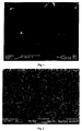
  • Fig.1 shows the surface morphology of a MTCVD Ti(C,N) according to the prior art using SEM at a magnification of 10000 times.
  • Fig.2 shows the surface morphology of a modified MTCVD Ti(C,N) coating according to this invention using SEM at a magnification of 10000 times.
  • Fig. 3 shows a high resolution FEG SEM image (magnification about 50000 times) of the surface of the coating according to this invention.
  • Fig. 4 shows a typical X-ray diffraction pattern of a coating according to this invention being composed of fine, columnar grains.
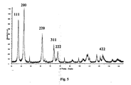
  • Fig. 5 shows a typical X-ray diffraction pattern of a coating composed of fine, equiaxed grains.
  • DETAILED DESCRIPTION OF THE PREFERRED EMBODIMENTS OF THE INVENTION
    It has surprisingly been found that controlled reduction of the grain size of the MTCVD layers simultaneously maintaining the columnar grain morphology enhances the wear resistance by more than 100% over the prior-art MTCVD coatings in carbon steels and cast iron. Especially important is that crater wear resistance is enhanced with maintained toughness. The coatings according to this invention increase the cutting performance at higher cutting speeds and can be combined with alumina layers to tailor-made a tool for extreme high-speed applications. The process can be performed in a controlled way by using modem CVD reactors from the typical MTCVD temperatures of the order of 800-900 °C up to 1000 °C.
    According to the present invention there is provided a cutting tool insert consisting of a substrate at least partially coated with a coating with a total thickness of 10-40 µm, preferably 15-25 µm consisting of one or more refractory layers of which at least one layer is a MTCVD-Ti(C,N)-layer with columnar grains with a thickness of 3 to 30 µm, preferably 5-20 µm. The columnar grains should have a width from 30-300 nm, preferably 50 to 200 nm and most preferably 50 to 100 nm. The L/W ratio (Length/Width) should be higher than 3, preferably higher than 5 and most preferably higher than 10. This kind of coating is consequently composed of fine, needle-like grains and shows clearly enhanced wear resistance. Wear resistance of these coatings may exceed that of the prior art MTCVD Ti(C,N) coating deposited from the TiCl4-CH3CN-N2-H2 system by up to several hundreds of percents.
    The said layer can be applied onto an α-Al2O3, κ-Al2O3 or γ-Al2O3 layer which itself has been deposited on top the said layer.
    The fine-grained, columnar morphology can be obtained by using extremely low and controlled levels of CO and/or ZrCl4 or HfCl4 doping. These dopants can be added simultaneously and preferably together with AlCl3. The amount of CO should be from 0.1 to 1.0% and most preferably from 0.2 to 0.8%. ZrCl4 and HfCl4 should be applied in the range of 0.1 to 0.5%, preferably from 0.2 to 0.3% and AlCl3 should be applied in the range of 0.5 to 3.0%, preferably from 1.0 to 1.5%. Very low amounts of CO2 can be used. In this case we want to avoid equiaxed grain morphology and, thus, CO2 should be used with extreme care. CO2 must be less than 0.1%, preferably from 0.01 to 0.08% of the total flow with a high CO/CO2 ratio. The CO/CO2 ratio should be higher than 8, preferably higher than 10 and if possible about 15. The deposition is performed at a temperature of from 700 to 1000°C, preferably 800-900°C.
    In Table 1 the effects of the additions of ZrCl4, HfCl4, AlCl3, CO or CO2 dopants in the TiCl4-CH3CN-N2-H2 system are depicted. The coatings were deposited at 880 °C and at a total pressure of 70 mbar.
    CO CO2 AlCl3 ZrCl4 HfCl4
    Columnar 0.1 - 1.0% -------- --------- -------- -------
    Columnar 0.1 - 1.0% -------- 1.0 - 2.0% -------- -------
    Columnar --------- -------- --------- 0.1 - 0.5% -------
    Columnar 0.1 - 1.0% -------- --------- 0.1 - 0.5% -------
    Columnar --------- -------- 1.0 - 2.0% 0.1 - 0.5% -------
    Columnar 0.1 - 1% -------- 1.0 - 2.0% 0.1 - 0.5% -------
    Columnar --------- --------- -------- -------- 0.1 - 0.5%
    Columnar 0.1 - 1.0% --------- -------- -------- 0.1 - 0.5%
    Equiaxed 1.5 - 4.0% --------- -------- -------- -------
    Equiaxed --------- 0.01 - 0.08% --------- --------- ------
    Equiaxed --------- --------- --------- 1.5 - 5.0% ------
    Equiaxed 1.5 - 4.0 --------- 2.5 - 5.5% -------- ------
    Equiaxed 1.5 - 4.0% 0.1 - 0.4 2.5 - 5.5% -------- -------
    Equiaxed 0.5 - 4.0% --------- --------- 1.5 - 3.5 % -------
    Equiaxed 0.5 - 4.0% 0.1 - 0.4 2.5 - 5.5% 1.5 - 3.5% -------
    Equiaxed 0.5 - 4.0% -------- --------- -------- 0.1 - 3.5%
    Equiaxed 0.5 - 4.0% 0.1 - 0.4 --------- -------- 0.1 - 3.5%
    According to this invention it has also been found to be possible to control and obtain a uniform columnar grain size in a coating layer independent on the total thickness of the said coating layer. As clear, for example, from US 6,221,469 the grain size depends on the coating thickness. Especially the prior-art CVD coatings show large variation in grain size: in the near vicinity of the substrate the coating may be composed of sub-micron grains while on top of the coating the grain size may be of the order of several micrometers.
    The present invention relates the cutting performance with the growth texture. The growth texture can be described by texture coefficients (TC), which are determined as follows:
    Figure 00050001
       where
  • I(hkl) = intensity of the (hkl) reflection
  • Io(hkl) = standard intensity according to JCPDS card no 42-1489
  • n = number of reflections used in the calculation
  • (hkl) reflections used are: (111), (200), (220), (311), (222), (400), (331), (420), (422), (511).
  • The texture coefficient for all coatings according to this invention should be as follows: The texture coefficient for 422 (TC(422)) should be higher than 5.0, preferably higher than 6 and most preferably higher than 7 or the texture coefficient for 331 (TC(331)) should be higher than 4, preferably higher than 5 and most preferably higher than 6.
    Further, line broadening of the 422 reflection should be less than 2.0 expressed as a relative value, the reference being non-doped prior-art Ti(C,N). Line broadening is defined as Bn/B0, where B0 is the Full Width at Half Maximum (FWHM) of the reference reflection and Bn is the Full Width at Half Maximum (FWHM) of the corresponding reflection of the coating according to this invention. Both are measured from Kα2- stripped Gaussian profiles of the 422 reflection.
    Line broadening is also a useful means to control that the produced layer has not been brought into the nanograined region manifested by strong line broadening. Expressed in absolute values (2°) the FWHM of either (422) or (331) diffraction peaks should be less than 1.5°, preferably less than 1.2° most preferably less than 1.0 °.
    Chemical compositions of the obtained layers can be described by the following formula (TixAlyXz)(CuOwNv), where x, u and v >0 and at least one of y, z and w >0. The compositions of the layers according to this invention should be varied in the following limits: x is from 0.3 to 0.8, y is from 0.0 to 0.1, z is from 0.0 to 0.1, u is from 0.3 to 0.9, w is from 0.0 to 0.1 and y is from 0.3 to 0.6. In the formula (TixAlyXz)(CuOwNv) X can be selected from groups 4 to 6. The useful elements are Zr, Hf, Nb, Ta or Mo even though Zr and Hf are used preferably.
    The substrate comprises a hard material such as cemented carbide, cermets, ceramics, high speed steel or a superhard material such as cubic boron nitride (CBN) or diamond preferably cemented carbide or CBN. With CBN is herein meant a cutting tool material containing at least 40 vol-% CBN. In a preferred embodiment the substrate is a cemented carbide with or without a binder phase enriched surface zone.
    Example 1
    In this case only CO and ZrCl4 were applied to obtain columnar structures with controlled, reduced, gain size. The following five experimental coatings (referred to as coatings 1, 2, 3, 4 and 5) were produced at a pressure of 70 mbar and at a temperature of 880°C according to the process data given in Table 2. Compared with the U.S. 6,472,060, considerably lower amounts of doping were used except coating 5, which was produced according to prior art U.S. 6,472,060. In order to achieve fine-grained columnar structure a maximum amount of CO should be less than 1%, preferably from 0.1 to 0.8%. In this example 0.8% of CO was used (Coating 2). Coating 3 was deposited at CO doping level of 2.5% to obtain equiaxed grain morphology. Coating 4 was deposited using ZrCl4 doping to obtain columnar morphology. Coating 5 was deposited using 8% CO according to U.S. 6,472,060 to obtain a nanograined layer. Coating 1 was deposited according to prior art without any dopant addition and is an example of a typical structure of a MTCVD coating.
    Cemented carbide cutting inserts with a composition of 6.0% Co and balance WC (hardness about 1580 HV) were used as substrates in all Examples. The following geometries were used in the cutting tests: SNUN120408 and CNMG120408-M3.
    H2 (1/min) N2 (1/min) CH3CN (1/min) TiCl4 (1/min) ZrCl4 (%) AlCl3(%) CO2(%) CO(%)
    Coating 1 balance 45.5 0.55 2.1 0.0 0.0 0.0 0.0
    Coating 2 balance 45.5 0.55 2.1 0.0 0.0 0.0 0.8
    Coating 3 balance 45.5 0.55 2.1 0.0 0.0 0.0 2.5
    Coating 4 balance 45.5 0.55 2.1 0.5 0.0 0.0 0.0
    Coating 5 balance 45.5 0.55 2.1 0.0 0.0 0.0 8.0
    Example 2
    The coatings from Example 1 were investigated using Transmission electron microscopy (TEM) and Scanning electron microscopy (SEM) in order to elucidate the effect of CO and ZrCl4 doping on the grain size and morphology. It appeared clear even in SEM that the microstructure of the typical MTCVD Ti(C,N) coating being composed of large columnar crystals (Fig. 1) can be refined by CO doping. The obtained layer was composed of needle like crystals as shown in Fig. 2 at a CO doping level of 0.8%. Similar surface morphologies could be obtained either by ZrCl4 or HfCl4 doping alone or together with CO. The equiaxed grain morphology was obtained at CO doping level of 2.5%. TEM revealed that at this CO level the grain size was not brought into the nanograined region and was about 60 nm. Coating 4, which was deposited using ZrCl4 doping was composed of columnar grains with slightly smaller needle-like grains than Coating 2. The grain size of Coating 5 was in the nanograined region. The results of the coating experiments are summarised in Table 3.
    Grain size Morphology
    Coating
    1 1500 x 4000 nm Large columnar
    Coating
    2 90 x 650 nm Needle-like
    Coating 3 60 nm Small-equiaxed
    Coating
    4 75 x 600 nm Needle-like
    Coating 5 14 nm Nanograined**)
    Example 3
    The following five experimental coatings (referred to as coatings 6, 7, 8, 9 and 10) were produced at a pressure of 70 mbar and at a temperature of 880°C according to the process data given in Table 4. The coating thickness was 8 µm for all coatings. CO2 was not used in this particular example but could be applied with extreme care because coatings can in the presence of this precursor easily be brought into the nanograined region with equiaxed grain size.
    The coatings were studied by using TEM together with EDS/WDS. The results are presented in Table 5. Surface morphology of Coating 9 is shown in Fig.3.
    H2 (1/min) N 2 1/(min) CH3CN (1/min) TiCl4 (1/min) ZrCl4 (%) AlCl3(%) CO2 (%) CO(%)
    Coating 6 balance 45.5 0.55 2.1 0.1 0.0 0.0 0.0
    Coating 7 balance 45.5 0.55 2.1 0.3 0.0 0.0 0.0
    Coating 8 balance 45.5 0.55 2.1 0.3 0.0 0.0 0.5
    Coating 9 balance 45.5 0.55 2.1 0.5 1.5 0.0 0.0
    Coating 10 balance 45.5 0.55 2.1 0.5 1.5 0.0 0.5
    Grain size Morphology Analysis
    Coating 6 70 x 650 nm Needle-like Traces of Zr
    Coating 7 55 x 750 nm Needle-like 1.32 wt % Zr
    Coating 8 45 x 820 nm Needle-like 1.33 wt % Zr
    Coating
    9 75 x 400 nm Needle-like 2.11 wt % Zr 0.91 wt % Al
    Coating 10 90 x 450 nm Needle-like 2.08 wt % Zr 1.22 wt% Al 1.22 wt% Al
    Example 4
    The coatings 1, 2, 3, 4 and 8 were studied using XRD. The texture coefficients were determined according to the following.
    Figure 00080001
       where
  • I(hkl) = intensity of the (hkl) reflection
  • Io(hkl) = standard intensity according to JCPDS card no 42-1489
  • n = number of reflections used in the calculation
  • (hkl) reflections used are: (111), (200), (220), (311), (222), (331) (420)(422)(511).
  • The results are given in Table 6.
    (h,k,l) Coating 1 Coating 2 Coating 3 Coating 4 Coating 8
    111 1.50 0.02 0.69 0.02 0.01
    200 0.05 0.00 0.54 0.00 0.00
    220 0.09 0.10 0.61 0.00 0.45
    311 0.21 0.05 0.72 0.05 0.02
    222 0.89 0.01 0.94 0.01 0.01
    400 0.03 0.01 0.36 0.03 0.00
    331 1.70 0.04 1.93 0.09 7.21
    420 0.73 0.05 1.59 0.05 0.65
    422 3.77 9.60 1.78 9.65 1.50
    511 1.04 0.11 0.84 0.12 0.14
    Example 5
    Coatings 1, 2, 4 and 8 were studied by using XRD. The grain refinement was slightly manifested as line broadening. XRD demonstrated that the coatings according to this invention are not in the nanograined region, Table 7.
    CO % FWHM (°2) Line broadening (Bn/B0) Grain Shape
    Coating
    1 0.541 (B0) 1.00 Large columnar
    Coating
    2 0.849 (Bn2 ) 1,57 columnar
    Coating
    4 0.860 (Bn4 ) 1.59 columnar
    Coating 8 0,924 (Bn8 ) 1.71 columnar
    Example 6
    Typical X-ray diffraction patterns originating from Coating 2 (Example 1) and Coating 3 (Example 1) are shown in Figs 4 and 5, respectively. Coating 2 (Fig. 4) is deposited according to this invention and is composed of needle-like grains with a strong 422-diffraction peak and Coating 3 (Fig. 5) is composed of small columnar grains. The differences are clear. XRD easily can be used to show that the coating is composed of columnar grains and not of equiaxed grains or visa versa. Further, XRD can be used to verify that the grain size is not brought into the nanograined region.
    Example 7
    The coatings produced in Example 1 were tested in carbon steel under the following conditions:
    Work piece Cylindrical bar
    Material SS1672
    Insert type SNUN120418
    Cutting speed 250 and 400 m/min
    Feed 0.5 mm/rev
    Depth of cut 2.5 mm
    Remarks Dry turning
    As can be seen from Table 8 the fine-grained columnar structures exhibited the best wear resistances. It should be noted that all the experimental coatings (also the equiaxed one, Coating 3) showed better wear resistance than the reference. Columnar fine-grained coatings clearly outperformed the prior-art. Zr-doped coating (Coating 4) exhibited the best performance. Nanograined layer (Coating 5) failed due to decreased crater wear resistance especially at the higher cutting speeds.
    Turning Carbon Steel (SS 1672)
    Life time (min) at 250 m/min Life time (min) at 400 m/min
    Coating
    1 5 2
    Coating 2 9 5
    Coating 3 7 3
    Coating 4 11 6
    Coating 5 3 1
    Example 8
    The experimental coatings from Examples 1 and 3 were compared in turning of carbon steel under the following conditions:
    Work piece Cylindrical bar
    Material SS1672
    Insert type CNMG 120418
    Cutting speed 250 and 400 m/min
    Feed 0.4 mm/rev
    Depth of cut 2.5 mm
    Remarks Dry turning
    Turning Carbon Steel (SS 1672)
    Life time (min) at 250 m/min Life time (min) at 400 m/min
    Coating
    1 5 2
    Coating 3 7 3
    Coating 6 8 4
    Coating 7 11 5
    Coating 8 11 5
    Coating 9 8 4
    Coating 10 9 5
    Results are shown in Table 9. All coatings composed of fine-grained columnar crystals outperformed the reference coating (Coating 1) composed of large columnar grains and also the coating composed of equiaxed grains (Coating 3). The coatings 7 and 8 with the highest L/W ratios were found to show the longest tool life.
    Example 9
    The experimental coatings from Examples 1 and 3 were compared in stainless steel (Table 10). All coatings according to this invention exhibited better wear resistance than the reference coating (Coating 1). However, in this material the coating composed of equiaxed grains (Coating 3) exhibited a better performance than the coatings having the columnar structure. Consequently, the columnar coatings should be preferred in carbon steels due to the much better wear resistance under those conditions. In stainless steel one should prefer equiaxed structures.
    Turning Stainless Steel (SS 2333)
    Life time (min) at 185 m/min Life time (min) at 250 m/min
    Coating
    1 5 2
    Coating 3 10 6
    Coating 4 8 5
    Coating 8 9 4
    Coating 9 8 5
    Coating 10 9 5

    Claims (8)

    1. Cutting tool insert consisting of a substrate of cemented carbide, cermet or ceramic at least partially coated with a coating with a total thickness of 10-40 µm, preferably 15-25 µm consisting of one or more refractory layers of which at least one layer is a MTCVD-Ti(C,N)-layer with a thickness of 3 to 30 µm, preferably 5-20 µm characterized in said layer being composed of columnar grains with grain width of 30-300 nm, preferably 50-200 nm and having a length-to-width ratio (L/W)≥3, preferably >5.
    2. Cutting tool insert according to claim 1 characterized in said at least one layer having texture coefficients of
      a) TC(422) > 5, preferably > 7
         or
      b) TC(331) > 5, preferably from > 6.
      wherein the texture coefficient TC(hkl) being defined as
      Figure 00130001
      where
      I(hkl) = measured intensity of the (hkl) reflection
      Io(hkl) = standard intensity according to JCPDS card no 42-1489
      n = number of reflections used in the calculation
      (hkl) reflections used are: (111), (200), (220), (311), (222), (400) (331) (420)(422)(511).
    3. Cutting tool insert according to any of the preceding claims characterized in said at least one refractory layer exhibits a line broadening of either (422) or (331) diffraction peaks expressed in absolute values (2°) of less than 1.5°, preferably less than 1.2°, most preferably less than 1.0° using CuKα-radiation.
    4. Cutting tool insert according to any of the preceding claims characterized in that said MTCVD-Ti(C,N)-layer is a (TixAlyXz)(CuOwNv) layer with the following composition: 0.3<x<0.8, 0.0<y<0.1, 0.0<z<0.1, 0.3<u<0.9, 0.0<w<0.1 and 0.3<v<0.6 X being selected from groups 4-6 being preferably Zr or Hf.
    5. Cutting tool insert according to any of the preceding claims characterized in said layer is applied onto an α-Al2O3, κ-Al2O3 or γ-Al2O3 layer which itself has been deposited on top the said layer.
    6. Method of depositing a MTCVD-Ti(C,N)-layer using known MTCVD-technique characterized in using a dopant addition in order to obtain a layer composed of columnar grains with grain width of 30-300 nm, preferably 50-200 nm and having a length-to-width ratio (L/W) of ≥ 3, preferably >5.
    7. Method according to claim 6 characterized in said dopant addition comprising
      CO in the range 0.1-1.0%, preferably from 0.2-0.8% of the total gas flow,
      CO2 in the range 0.01 - 0.1%, preferably 0.05 - 0.08 % with CO/CO2 ratio > 8, preferably > 10.
      an aluminium halide in the range 0.5-3.0%, preferably 1.0-1.5 %,
      a zirconium halide in the range 0.1-0.5%, preferably 0.2-0.3 % and/or
      a hafnium halide in the range 0.1-0.5%, preferably 0.2-0.3 %.
    8. Method according to claim 8 characterized that the zirconium halide is ZrCl4, the hafnium halide is HfCl4, the aluminium halide is AlCl3 and nitrogen and carbon are supplied by CH3CN and the deposition is performed at a temperature of from 700 to 1000°C.
    EP04009403A 2003-04-24 2004-04-21 Layer with controlled grain size and morphology for enhanced wear resistance Withdrawn EP1471166A3 (en)

    Applications Claiming Priority (2)

    Application Number Priority Date Filing Date Title
    SE0301196A SE527346C2 (en) 2003-04-24 2003-04-24 Cutter with coating of layers of MTCVD-Ti (C, N) with controlled grain size and morphology and method of coating the cutter
    SE0301196 2003-04-24

    Publications (2)

    Publication Number Publication Date
    EP1471166A2 true EP1471166A2 (en) 2004-10-27
    EP1471166A3 EP1471166A3 (en) 2007-08-29

    Family

    ID=20291109

    Family Applications (1)

    Application Number Title Priority Date Filing Date
    EP04009403A Withdrawn EP1471166A3 (en) 2003-04-24 2004-04-21 Layer with controlled grain size and morphology for enhanced wear resistance

    Country Status (5)

    Country Link
    US (2) US7192660B2 (en)
    EP (1) EP1471166A3 (en)
    KR (1) KR20040093037A (en)
    CN (1) CN100557077C (en)
    SE (1) SE527346C2 (en)

    Cited By (3)

    * Cited by examiner, † Cited by third party
    Publication number Priority date Publication date Assignee Title
    CN102653146A (en) * 2011-03-04 2012-09-05 钴碳化钨硬质合金公司 Coated substrates and methods of making same
    EP1825943B1 (en) 2004-12-14 2017-01-25 Sumitomo Electric Hardmetal Corp. Coated cutting tool
    DE102005049393B4 (en) 2005-10-15 2019-08-08 Kennametal Widia Produktions Gmbh & Co. Kg Method for producing a coated substrate body, substrate body with a coating and use of the coated substrate body

    Families Citing this family (35)

    * Cited by examiner, † Cited by third party
    Publication number Priority date Publication date Assignee Title
    JP4518258B2 (en) * 2004-08-11 2010-08-04 三菱マテリアル株式会社 A surface-coated cermet cutting tool that exhibits excellent chipping resistance with a hard coating layer in high-speed intermittent cutting
    US7597970B2 (en) * 2005-03-22 2009-10-06 Kyocera Corporation Surface coated member and cutting tool
    US8637127B2 (en) 2005-06-27 2014-01-28 Kennametal Inc. Composite article with coolant channels and tool fabrication method
    RU2432445C2 (en) 2006-04-27 2011-10-27 Ти Ди Уай Индастриз, Инк. Modular drill bit with fixed cutting elements, body of this modular drill bit and methods of their manufacturing
    US8080312B2 (en) * 2006-06-22 2011-12-20 Kennametal Inc. CVD coating scheme including alumina and/or titanium-containing materials and method of making the same
    EP2078101A2 (en) 2006-10-25 2009-07-15 TDY Industries, Inc. Articles having improved resistance to thermal cracking
    SE532023C2 (en) * 2007-02-01 2009-09-29 Seco Tools Ab Textured hardened alpha-alumina coated cutting for metalworking
    US20090004449A1 (en) * 2007-06-28 2009-01-01 Zhigang Ban Cutting insert with a wear-resistant coating scheme exhibiting wear indication and method of making the same
    US8080323B2 (en) * 2007-06-28 2011-12-20 Kennametal Inc. Cutting insert with a wear-resistant coating scheme exhibiting wear indication and method of making the same
    JP2009095907A (en) * 2007-10-15 2009-05-07 Sumitomo Electric Hardmetal Corp Blade edge replaceable cutting chip
    CN101952070B (en) * 2008-01-29 2013-03-13 京瓷株式会社 Cutting tool
    US8790439B2 (en) 2008-06-02 2014-07-29 Kennametal Inc. Composite sintered powder metal articles
    US8025112B2 (en) 2008-08-22 2011-09-27 Tdy Industries, Inc. Earth-boring bits and other parts including cemented carbide
    US9050673B2 (en) * 2009-06-19 2015-06-09 Extreme Surface Protection Ltd. Multilayer overlays and methods for applying multilayer overlays
    AT12293U1 (en) * 2009-10-05 2012-03-15 Ceratizit Austria Gmbh CUTTING TOOL FOR MACHINING METALLIC MATERIALS
    US9643236B2 (en) 2009-11-11 2017-05-09 Landis Solutions Llc Thread rolling die and method of making same
    US8734070B2 (en) 2010-10-20 2014-05-27 Kennametal Inc. Toolholder with externally-mounted dynamic absorber
    US8524360B2 (en) 2011-08-29 2013-09-03 Kennametal Inc. Cutting insert with a titanium oxycarbonitride coating and method for making the same
    US8800848B2 (en) 2011-08-31 2014-08-12 Kennametal Inc. Methods of forming wear resistant layers on metallic surfaces
    US9016406B2 (en) 2011-09-22 2015-04-28 Kennametal Inc. Cutting inserts for earth-boring bits
    WO2013081047A1 (en) * 2011-11-29 2013-06-06 京セラ株式会社 Coated tool
    EP2604720A1 (en) * 2011-12-14 2013-06-19 Sandvik Intellectual Property Ab Coated cutting tool and method of manufacturing the same
    IN2015DN01831A (en) * 2012-10-01 2015-05-29 Hitachi Tool Eng
    WO2014198881A1 (en) * 2013-06-14 2014-12-18 Sandvik Intellectual Property Ab Coated cutting tool
    EP3099912A4 (en) 2014-01-28 2017-02-01 United Technologies Corporation Ceramic covered turbine components
    RU2704949C2 (en) 2014-12-19 2019-10-31 Сандвик Интеллекчуал Проперти Аб Cvd coated cutting tool
    KR101687142B1 (en) * 2016-07-20 2016-12-15 한국야금 주식회사 Hard coated layer for cutting tools
    JP6481897B2 (en) * 2016-09-16 2019-03-13 三菱マテリアル株式会社 Surface coated cutting tool
    CN109963674B (en) * 2016-11-17 2021-07-06 株式会社泰珂洛 Coated Cutting Tools
    EP3366796A1 (en) * 2017-02-28 2018-08-29 Sandvik Intellectual Property AB Coated cutting tool
    RU2760426C2 (en) * 2017-04-07 2021-11-25 Сандвик Интеллекчуал Проперти Аб Cutting tool equipped with coating
    US12465980B2 (en) 2019-08-30 2025-11-11 Seco Tools Ab Coated cutting tool
    JP7141601B2 (en) * 2019-12-19 2022-09-26 株式会社タンガロイ coated cutting tools
    CN112342525B (en) * 2020-10-20 2023-04-28 厦门金鹭特种合金有限公司 CVD (chemical vapor deposition) coating suitable for vermicular cast iron cutting processing and preparation method thereof
    CN117178079B (en) * 2021-04-23 2026-04-24 山特维克科洛曼特公司 Cutting tools

    Family Cites Families (25)

    * Cited by examiner, † Cited by third party
    Publication number Priority date Publication date Assignee Title
    SE406090B (en) 1977-06-09 1979-01-22 Sandvik Ab COATED HARD METAL BODY AND WAY TO PRODUCE A SUITABLE BODY
    USRE31256E (en) * 1978-01-18 1983-05-31 Automatic damper means and controls therefor
    US4619866A (en) * 1980-07-28 1986-10-28 Santrade Limited Method of making a coated cemented carbide body and resulting body
    US4357382A (en) * 1980-11-06 1982-11-02 Fansteel Inc. Coated cemented carbide bodies
    JPS60200250A (en) * 1984-03-23 1985-10-09 Fuji Photo Film Co Ltd Formation of high-contrast negative image
    CH669347A5 (en) * 1986-05-28 1989-03-15 Vni Instrument Inst
    JP3136778B2 (en) * 1992-06-11 2001-02-19 三菱マテリアル株式会社 Surface coated titanium carbonitride based cermet cutting tool with excellent chipping resistance
    JP3109306B2 (en) * 1992-11-25 2000-11-13 三菱マテリアル株式会社 Surface-coated cermet cutting tool with improved wear resistance of hard coating layer
    JP3278785B2 (en) * 1993-08-27 2002-04-30 三菱マテリアル株式会社 Manufacturing method of surface coated cutting tool
    US5496762A (en) * 1994-06-02 1996-03-05 Micron Semiconductor, Inc. Highly resistive structures for integrated circuits and method of manufacturing the same
    JPH08132130A (en) * 1994-11-10 1996-05-28 Mitsubishi Materials Corp Surface coated cermet drawing dies with excellent adhesion of hard coating layer
    SE514181C2 (en) * 1995-04-05 2001-01-15 Sandvik Ab Coated carbide inserts for milling cast iron
    SE514177C2 (en) * 1995-07-14 2001-01-15 Sandvik Ab Coated cemented carbide inserts for intermittent machining in low alloy steel
    US5981078A (en) * 1995-08-19 1999-11-09 Widia Gmbh Composite body and process for its production
    JP3250134B2 (en) * 1995-12-25 2002-01-28 三菱マテリアル株式会社 Surface coated cemented carbide cutting tool with excellent chipping resistance
    SE509560C2 (en) * 1996-09-06 1999-02-08 Sandvik Ab Coated cemented carbide inserts for machining cast iron
    DE69730576T2 (en) * 1996-12-04 2005-02-03 Sumitomo Electric Industries, Ltd. Coated tool and method for its manufacture
    SE511211C2 (en) * 1996-12-20 1999-08-23 Sandvik Ab A multilayer coated polycrystalline cubic boron nitride cutting tool
    US20010016273A1 (en) * 1998-05-08 2001-08-23 Krishnan Narasimhan Multilayer cvd coated article and process for producing same
    DE69901985T2 (en) * 1998-07-29 2002-12-05 Toshiba Tungaloy Co. Ltd., Kawasaki Tool part coated with aluminum oxide
    US6221469B1 (en) * 1998-12-09 2001-04-24 Seco Tools Ab Grade for steel
    US6251508B1 (en) * 1998-12-09 2001-06-26 Seco Tools Ab Grade for cast iron
    DE19962056A1 (en) * 1999-12-22 2001-07-12 Walter Ag Cutting tool with multi-layer, wear-resistant coating
    US6472060B1 (en) * 2000-01-19 2002-10-29 Seco Tools Ab Coated body with nanocrystalline CVD coating for enhanced edge toughness and reduced friction
    EP1323847A3 (en) * 2001-12-28 2005-09-14 Seco Tools Ab Coated cemented carbide body and method for use

    Cited By (4)

    * Cited by examiner, † Cited by third party
    Publication number Priority date Publication date Assignee Title
    EP1825943B1 (en) 2004-12-14 2017-01-25 Sumitomo Electric Hardmetal Corp. Coated cutting tool
    DE102005049393B4 (en) 2005-10-15 2019-08-08 Kennametal Widia Produktions Gmbh & Co. Kg Method for producing a coated substrate body, substrate body with a coating and use of the coated substrate body
    CN102653146A (en) * 2011-03-04 2012-09-05 钴碳化钨硬质合金公司 Coated substrates and methods of making same
    CN102653146B (en) * 2011-03-04 2016-05-04 钴碳化钨硬质合金公司 The matrix and the manufacture method thereof that apply

    Also Published As

    Publication number Publication date
    CN1570202A (en) 2005-01-26
    CN100557077C (en) 2009-11-04
    US7192660B2 (en) 2007-03-20
    US20070110897A1 (en) 2007-05-17
    US7718226B2 (en) 2010-05-18
    KR20040093037A (en) 2004-11-04
    SE527346C2 (en) 2006-02-14
    EP1471166A3 (en) 2007-08-29
    SE0301196L (en) 2004-10-25
    SE0301196D0 (en) 2003-04-24
    US20050013995A1 (en) 2005-01-20

    Similar Documents

    Publication Publication Date Title
    US7192660B2 (en) Layer with controlled grain size and morphology for enhanced wear resistance
    US7927663B2 (en) Method of forming a coating with controlled grain size and morphology for enhanced wear resistance and toughness
    RU2062260C1 (en) Sintered article
    EP1953258B1 (en) Texture-hardened alpha-alumina coated tool
    EP0850324B1 (en) Coated turning insert
    US6652913B2 (en) Method of forming a coated body having a nanocrystalline CVD coating of Ti(C,N,O)
    US6713172B2 (en) Oxide coated cutting tool
    EP0871796B1 (en) Coated milling insert and method of making it
    EP1528125B1 (en) Coated cutting insert for rough turning
    EP1655392B1 (en) Alumina layer with enhanced texture
    EP1655387B1 (en) Enhanced alumina layer with texture
    EP2604720A1 (en) Coated cutting tool and method of manufacturing the same
    EP1262576B1 (en) CVD Al2O3 coated cutting tool
    CN115786875B (en) Coating with enhanced toughness and wear resistance, and preparation method and application thereof

    Legal Events

    Date Code Title Description
    PUAI Public reference made under article 153(3) epc to a published international application that has entered the european phase

    Free format text: ORIGINAL CODE: 0009012

    AK Designated contracting states

    Kind code of ref document: A2

    Designated state(s): AT BE BG CH CY CZ DE DK EE ES FI FR GB GR HU IE IT LI LU MC NL PL PT RO SE SI SK TR

    AX Request for extension of the european patent

    Extension state: AL HR LT LV MK

    PUAL Search report despatched

    Free format text: ORIGINAL CODE: 0009013

    AK Designated contracting states

    Kind code of ref document: A3

    Designated state(s): AT BE BG CH CY CZ DE DK EE ES FI FR GB GR HU IE IT LI LU MC NL PL PT RO SE SI SK TR

    AX Request for extension of the european patent

    Extension state: AL HR LT LV MK

    17P Request for examination filed

    Effective date: 20070907

    AKX Designation fees paid

    Designated state(s): AT BE BG CH CY CZ DE DK EE ES FI FR GB GR HU IE IT LI LU MC NL PL PT RO SE SI SK TR

    17Q First examination report despatched

    Effective date: 20101029

    STAA Information on the status of an ep patent application or granted ep patent

    Free format text: STATUS: THE APPLICATION IS DEEMED TO BE WITHDRAWN

    18D Application deemed to be withdrawn

    Effective date: 20131008