EP1468484B1 - Convertisseur de tension dc/dc multicellule a interrupteurs de protection - Google Patents
Convertisseur de tension dc/dc multicellule a interrupteurs de protection Download PDFInfo
- Publication number
- EP1468484B1 EP1468484B1 EP03717348A EP03717348A EP1468484B1 EP 1468484 B1 EP1468484 B1 EP 1468484B1 EP 03717348 A EP03717348 A EP 03717348A EP 03717348 A EP03717348 A EP 03717348A EP 1468484 B1 EP1468484 B1 EP 1468484B1
- Authority
- EP
- European Patent Office
- Prior art keywords
- transistor
- converter
- voltage
- terminals
- cell
- Prior art date
- Legal status (The legal status is an assumption and is not a legal conclusion. Google has not performed a legal analysis and makes no representation as to the accuracy of the status listed.)
- Expired - Lifetime
Links
Images





Classifications
-
- H—ELECTRICITY
- H02—GENERATION; CONVERSION OR DISTRIBUTION OF ELECTRIC POWER
- H02M—APPARATUS FOR CONVERSION BETWEEN AC AND AC, BETWEEN AC AND DC, OR BETWEEN DC AND DC, AND FOR USE WITH MAINS OR SIMILAR POWER SUPPLY SYSTEMS; CONVERSION OF DC OR AC INPUT POWER INTO SURGE OUTPUT POWER; CONTROL OR REGULATION THEREOF
- H02M1/00—Details of apparatus for conversion
- H02M1/32—Means for protecting converters other than automatic disconnection
-
- H—ELECTRICITY
- H02—GENERATION; CONVERSION OR DISTRIBUTION OF ELECTRIC POWER
- H02M—APPARATUS FOR CONVERSION BETWEEN AC AND AC, BETWEEN AC AND DC, OR BETWEEN DC AND DC, AND FOR USE WITH MAINS OR SIMILAR POWER SUPPLY SYSTEMS; CONVERSION OF DC OR AC INPUT POWER INTO SURGE OUTPUT POWER; CONTROL OR REGULATION THEREOF
- H02M3/00—Conversion of DC power input into DC power output
- H02M3/02—Conversion of DC power input into DC power output without intermediate conversion into AC
- H02M3/04—Conversion of DC power input into DC power output without intermediate conversion into AC by static converters
- H02M3/10—Conversion of DC power input into DC power output without intermediate conversion into AC by static converters using discharge tubes with control electrode or semiconductor devices with control electrode
- H02M3/145—Conversion of DC power input into DC power output without intermediate conversion into AC by static converters using discharge tubes with control electrode or semiconductor devices with control electrode using devices of a triode or transistor type requiring continuous application of a control signal
- H02M3/155—Conversion of DC power input into DC power output without intermediate conversion into AC by static converters using discharge tubes with control electrode or semiconductor devices with control electrode using devices of a triode or transistor type requiring continuous application of a control signal using semiconductor devices only
-
- H—ELECTRICITY
- H02—GENERATION; CONVERSION OR DISTRIBUTION OF ELECTRIC POWER
- H02M—APPARATUS FOR CONVERSION BETWEEN AC AND AC, BETWEEN AC AND DC, OR BETWEEN DC AND DC, AND FOR USE WITH MAINS OR SIMILAR POWER SUPPLY SYSTEMS; CONVERSION OF DC OR AC INPUT POWER INTO SURGE OUTPUT POWER; CONTROL OR REGULATION THEREOF
- H02M3/00—Conversion of DC power input into DC power output
- H02M3/02—Conversion of DC power input into DC power output without intermediate conversion into AC
- H02M3/04—Conversion of DC power input into DC power output without intermediate conversion into AC by static converters
- H02M3/10—Conversion of DC power input into DC power output without intermediate conversion into AC by static converters using discharge tubes with control electrode or semiconductor devices with control electrode
- H02M3/145—Conversion of DC power input into DC power output without intermediate conversion into AC by static converters using discharge tubes with control electrode or semiconductor devices with control electrode using devices of a triode or transistor type requiring continuous application of a control signal
- H02M3/155—Conversion of DC power input into DC power output without intermediate conversion into AC by static converters using discharge tubes with control electrode or semiconductor devices with control electrode using devices of a triode or transistor type requiring continuous application of a control signal using semiconductor devices only
- H02M3/156—Conversion of DC power input into DC power output without intermediate conversion into AC by static converters using discharge tubes with control electrode or semiconductor devices with control electrode using devices of a triode or transistor type requiring continuous application of a control signal using semiconductor devices only with automatic control of output voltage or current, e.g. switching regulators
- H02M3/158—Conversion of DC power input into DC power output without intermediate conversion into AC by static converters using discharge tubes with control electrode or semiconductor devices with control electrode using devices of a triode or transistor type requiring continuous application of a control signal using semiconductor devices only with automatic control of output voltage or current, e.g. switching regulators including plural semiconductor devices as final control devices for a single load
- H02M3/1584—Conversion of DC power input into DC power output without intermediate conversion into AC by static converters using discharge tubes with control electrode or semiconductor devices with control electrode using devices of a triode or transistor type requiring continuous application of a control signal using semiconductor devices only with automatic control of output voltage or current, e.g. switching regulators including plural semiconductor devices as final control devices for a single load with a plurality of power processing stages connected in parallel
Definitions
- the present invention relates to a voltage converter continuous / DC (DC / DC), and finds applications, in particular, in the automotive field.
- DC / DC voltage converter continuous / DC
- Such a converter is disclosed in the document US 6,275,958 B1.
- each cell is a DC / DC converter to cutting, which has the distinction of being uninsulated.
- Such a switching converter is an electrical device controlled quadrupole, comprising a first positive pair of terminals and negative on the one hand, and a second pair of positive and negative terminals on the other hand.
- the first and second negative terminals are connected together by a first determined circuit branch.
- the first and second positive terminals are connected together by a second branch of determined circuit, which comprises an inductance forming a reservoir of energy.
- the converter further comprises cutting means comprising at least one controlled switch, whose opening and closing are controlled by a management unit according to a specific duty cycle.
- Such a circuit is capable of delivering a continuous electric current or quasi-continuous between the first two positive and negative terminals according to a determined voltage, called output voltage, when a determined voltage, called input voltage, is applied between the second positive and negative terminals, or vice versa.
- the converter is said to be non-isolated in that it comprises the said first and second circuit branches connecting said first and second terminals, respectively negative and positive.
- Such a converter opposes indeed to an isolation converter, in which the first pair of terminals is isolated from the second pair of terminals.
- These transistors function as controlled switches that are closed during normal operation and are open when malfunction is detected.
- the dedicated components protection function are the cause of a static consumption of which, depending on the case, may vary between 0.5% and 2.0% of the static consumption of the entire device.
- An object of the present invention is to propose a converter of multi-cell voltage comprising a degraded operating mode, in which a particular cell can be neutralized independently of other cells when a malfunction occurs in that cell, any by minimizing consumption during normal operation.
- the transistor of unique protection of each cell is mounted in a high voltage part of the converter. Due to the high voltage the holding current in closed position is lower so the consumption is still minimized.
- Closed switch means a switch in a state such that is passing for the current flowing in the circuit branch containing this light switch. Conversely, an open switch imposes a zero intensity in the circuit branch to which it belongs.
- the switch is realized by means of a transistor which comprises a diode of structure
- the state open of this switch imposes a zero intensity when the voltage at terminals of the switch further causes the blocking of the structure diode, that is to say when the electrical potential of the cathode of this diode is greater than the electrical potential of the anode of this diode.
- the converter in connection with a transistor per cell mounted in a high voltage part of the converter, the converter further comprises a protection transistor common to all the cells associated with a low voltage part of the converter. So while Increasing very little the static consumption of the converter, it is protected against a polarity inversion in the low network voltage, especially during an inverted installation of a low voltage battery.
- a DC and high-current network voltage is connected to a buck converter by the terminal positive 1 and the negative 2.
- the voltage between terminals 1 and 2 is example located around 42 volts.
- DC and low-voltage network voltage is connected to terminals 3 and 4, terminal 3 being positive and terminal 4 being negative, and the voltage between these two terminals being for example located around 14 volts.
- a capacitor 16, 26, ..., 66 for example of 30 microfarads, connects the terminals 1 and 2 to store, on the 42-volt grid side, the electrical charges transferred by this elementary converter 100, 200, ..., 600.
- another capacitor 17, 27, ..., 67 for example also of 30 microfarads, connects terminals 3 and 4 in order to on the 14-volt grid side, the electrical charges transferred by this elementary converter 100, 200, ..., 600.
- Each elementary voltage-reducing converter 100, 200, ..., 600 further comprises a diode 12a, 22a, ..., 62a connected by its cathode to the node N1, N2, ..., N6 and its anode at terminals 2 and 4.
- Each of the elementary step-down converters 100, 200, ..., 600 thus constituted can transfer approximately a power from 250 watts of the 42-volt network to the 14-volt network.
- Figure 2 shows the converter control architecture elementary 100 of FIG. 1. It comprises a controller C1 receiving on its inputs said high voltage by the son 101 and 102 respectively connected at terminals 1 and 2, said low voltage by wire 103 connected to terminal 3 and the voltage across the resistor 15 by the wires 150 and 151.
- pulse width modulated control device known to the human the controller C1 controls the step-down transistor 11 by signals opening or closing transmitted to its gate by the wire 110, according to a determined periodicity of pulses, corresponding for example to a frequency of 70 kilohertz.
- a controller analogous to the controller C1 is arranged in the same way in each of the other five elementary converters 200, ..., 600 for perform an identical function vis-à-vis each of these circuits.
- the six controllers emit respective impulses according to the same periodicity of pulses, and are considered according to an order cyclic determined, so that pulses of two converters successive elementary elements in that order are shifted by a time equal to sixth of the control pulse period of each converter elementary.
- a detector D1 receives on two of its inputs the voltage between the drain and the source of the step-down transistor 11 by the two wires 111 and 112. In normal operation of the converter elementary 100, the detector D1 transmits a signal to a management unit of protection P so that it applies by the wire 130 a certain voltage at the gate of the protective transistor 13, for example a voltage between 5 and 10 volts with respect to the source of this transistor of protection 13, so as to keep the protective transistor 13 in a state closed, or passing.
- the detector D1 When the detector D1 identifies a transistor malfunction step 11, and in particular a short circuit between the drain and the source of this step-down transistor 11, the detector D1 interrupts the voltage applied to the gate of the protection transistor 13 by the wire 130, so as to open the circuit between the drain and the source of this protective transistor 13.
- This opening of circuit can be obtained by a polarization resistor, not shown and for example 10 kiloohms, connecting the gate and the source of the transistor of 13.
- a potential discharge current from the 42-volt network to the 14-volt network, by the elementary converter 100 can not flow from terminal 1 to terminal 3.
- the other elementary converters 200, ..., 600 also comprise each a respective detector D2, ..., D6 identical to the detector D1, and connected by similar to the P protection management unit.
- the latter is also connected by wires 230,..., 630 to the respective step-down transistors 23, ..., 63 elementary converters 200, ..., 600, so as to provide a same personal protection mechanism as all converters elementals 100, 200, ..., 600.
- Each elementary converter 100, 200, ..., 600 being arranged in Parallel with other elementary converters, shutting down operation of one of them does not interrupt the operation of others.
- a The operation of the global converter is therefore continued by means of elementary converters still operational. This pursuit of operation is permitted thanks to the parallel arrangement of elementary converters, as well as by the provision, according to this invention, a protection switch in each converter elementary.
- control mode of all the elementary converters 100, 200, ..., 600 by their respective controllers can be adapted by an unrepresented supervisor controller connected to the six controllers and six detectors, so as to take into account the neutralization of one of the elementary converters. This allows, in this circumstance, to optimize the operation of the overall converter despite stopping one of the elementary converters.
- the supervisor controller controls the controllers of the other five elementary converters 100, 200, ..., 600 still operational for the control pulses of two successive elementary converters staggered by a period equal to one-fifth of the common control pulses of each elementary converter.
- the degraded operation thus obtained for the overall converter, following the neutralization of one of the elementary converters, corresponds to a reduction of the maximum electric charge rate, or of the power electrical power, which can be transferred between the high voltage network and the low voltage network.
- FIG. 3 corresponds to an embodiment of the invention which consists of a step-up converter. This embodiment takes over the architecture and some of the components of the embodiment previous. The detailed description is not repeated in its entirety, and all components and references not listed are identical to those presented in the previous embodiment.
- the single protection transistor 12, 23, ...., 63 is mounted in the high voltage portion of the cell.
- each converter elementary element 100, 200, ..., 600 comprises an upstanding transistor 12, 22, ..., 62.
- This rising transistor 12, 22, ..., 62 for example still MOS-FET n-channel (N-MOS), is connected by its drain to the node N1, N2, ..., N6 and by its source to terminals 2 and 4.
- This boost transistor 12, 22, ..., 62 also comprises a diode with structure 19, 29, ..., 69 arranged in parallel and oriented in the direction passing to the node N1, N2, ..., N6.
- the operating mode of such an up-converter is known to those skilled in the art, and uses a control mode of transistors 12, 22, ..., 62 similar to that used in the previous embodiment for the step-down transistors.
- Each of the elementary step-up converters 100, 200, ..., 600 as well formed, can transfer approximately 250 watts of power from the 14-volt network to the 42-volt network.
- malfunction detectors D1, D2, ..., D6 are each connected by two inputs to the drain and the source of the transistor elevator 12, 22, ..., 62 of the elementary converter with which it is associated. These malfunction detectors D1, D2, ..., D6 participate in the same way than previously at the opening of the protective transistor 13, 23, ..., 63 of the elementary converter in which a malfunction is detected.
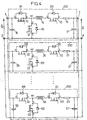
- Figure 4 corresponds to a converter composed of converters elementary 100, 200, ..., 600 reversible.
- Each of the converters elementary 100, 200, ..., 600 reversible takes components of step-down or step-up switching converters already presented, and arranged in a similar way. The detailed description of these components is not repeated here.
- Each elementary converter 100, 200, ..., 600 reversible comprises a step-down transistor 11, 21, ..., 61 and a boost transistor 12, 22, ..., 62 in the respective place of the diodes 11a, 21a, ..., 61a and 12a, 22a, ..., 62a.
- the step-down transistor 11, 21, ..., 61 for example MOS-FET n-channel (N-MOS), is connected by its drain to terminal 1 and by its source to node N1, N2, ..., N6. Its diode of structure 18, 28, ..., 68, placed in parallel with this step-down transistor 11, 21, ..., 61 is oriented in the forward direction of the terminal 3 to terminal 1.
- N-MOS MOS-FET n-channel
- the rising transistor 12, 22, ..., 62 for example still MOS-FET at channel n (N-MOS), is connected by its drain to the node N1, N2, ..., N6 and by its source at terminals 2 and 4. Its structure diode 19, 29, ..., 69 arranged in parallel is oriented in the direction towards the node N1, N2, ..., N6.
- the controller C1 has two outputs 110 and 120 connected respectively to the gate of the step-down transistor 11, 21, ..., 61 and to that of the transistor 12, 22, ..., 62 of this elementary converter 100. also has two inputs connected by wires 150 and 151 to the two terminals of the shunt resistor 15.
- the C1 controller in a mode of operation in a step-down mode. voltage the gate of the step-down transistor 11, 21, ..., 61 to open or close alternatively this one as a function of the value of the current measured in the shunt resistor 15. It simultaneously controls the gate of the transistor elevator 12, 22, ..., 62 so that it is open at least during the intervals of time during which the step-down transistor 11, 21, ..., 61 is closed.
- the controller C1 controls the gate of the boost transistor 12, 22, ..., 62 to open or close alternately depending on the value of the current measured in the shunt resistor 15. simultaneously the gate of the step-down transistor 11, 21, ..., 61 so that it open at least during the time intervals during which the lift transistor 12, 22, ..., 62 is closed.
- each reversible elementary converter 100, 200, .., 600 comprises a control system of the step-down transistor 11, 21, ..., 61 and elevator 12, 22, ..., 62 that it includes identical to that of reversible elementary converter 100. Synchronization of commands of all the reversible elementary converters is identical to that of step-down or step-up converters already described in the previous realization.
- the protection transistor 13, 23, ..., 63 of each elementary reversible converter 100, 200, ..., 600 is disposed between the inductor 14, 24, ..., 64 and the shunt resistor 15, 25, ..., 65, its drain being connected to the inductor, its source to the resistor, and its structure diode 20 oriented from terminal 3 to terminal 1.
- These protection transistors 13, 23, ..., 63 thus arranged are controlled by the protection management unit P (see FIG. 5), itself associated with the malfunction detectors D1, D2, ..., D6.
- These detectors D1, D2,..., D6 are respectively connected to the source and the draining step-down transistors 11, 21, ..., 61 of each converter elementary 100, 200 ...., 600.
- the protection obtained is then identical to that of the first embodiment, corresponding to Figures 1 and 2.
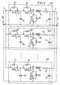
- FIGS. 6 and 7, associated with each other, correspond to a reversible converter with the same structure as the converter reversible shown in Figures 4 and 5.
- the protection transistor 13, 23, ..., 63 of each elementary reversible converter 100, 200, ..., 600 is disposed between the terminal 1 and the step-down transistor 11, 21, ..., 61. Its drain is connected to the terminal 1, and its source at an intermediate node between the transistor drain step-down 11, 21, ..., 61 and the capacitor 16, 26, .., 66.
- the diode of structure 20, 30, ..., 70 of the protective transistor 13, 23, ..., 63 is still oriented to pass in the direction of terminal 1.
- This position of the protection transistor 13, 23, ..., 63 is preferred over a position between the step-down transistor 11, 21, ..., 61 and a node of connection of the capacitor 16, 26, ..., 66 to the terminal 1.
- the current flowing in the loop formed by the capacitor 16, 26, ..., 66, the transistor step-down 11, 21, ..., 61 and the boost transistor 12, 22, ..., 62 being a current cut with sudden variations, it is particularly advantageous to reduce the physical dimension this loop in order to decrease the disturbances due to a possible parasitic self-inductance of this loop, or due to a eventual radiation emitted by this loop.
- the detector D1 still receives on its two inputs the voltage between the drain and the source of the step-down transistor 11 by the two wires 111 and 112. identical arrangement of these components is repeated for each of the reversible elementary converters 100, 200, ..., 600.
- FIG. 8 illustrates a device which is furthermore equipped with a transistor protection common to all cells on the low voltage side.
- cells 100 ... 600 have only been represented according to a dashed line, the individual structure of the cells being able to be one any of those described above, with incorporation of unique protection of each cell on the high voltage side.
- a high-current DC network voltage for example having a voltage of 42 volts between terminals H1 and H2, includes a battery HR arranged between these terminals.
- H1 is a positive terminal
- H2 is a negative terminal.
- a low voltage DC network for example 14 volts approximately between two terminals B3 and B4 of this network B, comprises a BR battery.
- the BR battery is connected between terminals B3 and B4.
- B3 is a positive terminal and B4 is a negative terminal.
- the low voltage network is connected via a filter 800 to cells 100, ... 600.
- Filter 800 is connected to terminals 3 and 4 common to the cells 100, ..., 600.
- the constitution of the filter 800 known from the skilled person, is not detailed here.
- the high voltage network is also connected to the cells through another filter 700 connected to terminals 1 and 2 on the one hand and to terminals H1, H2 of the high voltage network between which is connected a HR high voltage battery.
- a protective transistor 801 still with a field effect of the metal-oxide-semiconductor type (MOS-FET) N-channel (N-MOS) is arranged between the filter 800 and terminal B3.
- MOS-FET metal-oxide-semiconductor type
- N-MOS N-oxide-semiconductor type N-channel
- a control unit CS has an output connected to the gate of the protection transistor 801, and an input connected to an output of a detector D. This detector D is also connected to terminals B3 and B4.
- the D detector In normal operating mode, the D detector detects a voltage of the order of 14 volts between terminals B3 and B4. The CS control unit then controls the closing of the safety transistor 801 by application a positive voltage at its gate, of the order of 5 to 10 volts for example by report to its source.
- the control circuit CS interrupts the positive voltage applied to the gate of the protective transistor 801.
- a resistor 802 for example 10 kilohms, arranged between the gate and the source of the protective transistor 801, then ensures the opening of this transistor.
- the protective transistor 801 when it has a field effect of the type n-metal oxide-semiconductor (N-MOS), has a diode of external structure 803 arranged in parallel between the drain and the source of this transistor. This diode of structure 803 is passing in the direction from source to the drain of transistor 801, with a threshold voltage of the order of 0.9 volts at 1.3 volts.
- the protective transistor 801 is oriented so that the diode of structure 803 is passing in the direction of the filter 800.
- the invention has been described according to a preferred embodiment of disposing the single protection transistor of each cell on the high voltage side and the common switch on the low side voltage, which makes it possible to isolate a cell and to protect the converter against a polarity inversion on the low voltage side while having a consumption minimum static
- the protective transistors can be arranged in each cell on the low voltage side and the common switch on the high voltage side. At price of a slight increase in static consumption this allows avoid a charge transfer from the low voltage battery to the battery high voltage when the high voltage battery is discharged.
- the N-MOS type transistors can be replaced by transistors P-MOS type counterparts. They can also be replaced by Bipolar technology transistors, without the function and function general assembly are changed.
- the protective transistor that is common to all cells can also be replaced by a switch controlled by an electromagnetic relay.
- protective transistor 801 common to different cells on the low-voltage side have been shown in an integrated converter, it can be deported in relation to this one.
- control unit CS of transistor 801 has been illustrated separate from the protection management unit P, it can be incorporated to this one.
Landscapes
- Engineering & Computer Science (AREA)
- Power Engineering (AREA)
- Dc-Dc Converters (AREA)
- Charge And Discharge Circuits For Batteries Or The Like (AREA)
- Protection Of Static Devices (AREA)
- Semiconductor Integrated Circuits (AREA)
Description
- une première borne positive et une première borne négative destinées à être connectées respectivement à deux bornes d'un réseau électrique à haute tension ;
- une seconde borne positive et une seconde borne négative destinées à être connectées respectivement à deux bornes d'un réseau électrique à basse tension ;
- n cellules connectées en parallèle, où n est un nombre entier strictement supérieur à l'unité, disposées entre lesdites premières bornes positive et négative d'une part et lesdites secondes bornes positive et négative d'autre part, comprenant chacune un convertisseur DC/DC à découpage, ayant chacune une première branche de circuit reliant ladite première borne négative et ladite seconde borne négative, une deuxième branche de circuit comprenant une inductance et reliant ladite première borne positive et ladite seconde borne positive, des moyens de découpage comprenant au moins un interrupteur de découpage, et une unité de gestion adaptée pour commander l'ouverture et la fermeture de l'interrupteur de découpage selon un rapport cyclique déterminé ; dans lequel chaque cellule comporte en outre un transistor de protection unique disposé dans ladite seconde branche de circuit et associé à une unité de gestion de protection pour neutraliser ladite cellule indépendamment des autres cellules.
- la figure 1 est un schéma électrique d'un mode de réalisation d'un convertisseur abaisseur de tension selon la présente invention ;
- la figure 2 représente l'agencement d'un contrôleur et d'un détecteur de dysfonctionnement associés au convertisseur de la figure 1 ;
- la figure 3 est un schéma électrique d'un mode de réalisation d'un convertisseur élévateur de tension selon la présente invention ;
- la figure 4 est un schéma électrique d'un premier mode de réalisation d'un convertisseur abaisseur/élévateur de tension selon la présente invention ;
- la figure 5 représente l'agencement d'un contrôleur et d'un détecteur de dysfonctionnement associés au convertisseur de la figure 4 ;
- la figure 6 est un schéma électrique d'un second mode de réalisation d'un convertisseur abaisseur/élévateur de tension selon la présente invention ;
- la figure 7 représente l'agencement d'un contrôleur et d'un détecteur de dysfonctionnement associés au convertisseur de la figure 6,
- la figure 8 est un schéma électrique d'un dispositif comprenant une protection commune du côté basse tension.
- un transistor abaisseur 11, 21,..., 61, par exemple MOS-FET à canal n (N-MOS), connecté par son drain à la borne 1. Un tel transistor comporte une diode de structure 18, 28,..., 68 placée en parallèle avec l'interrupteur constitué par le transistor abaisseur 11, 21,..., 61, et orientée dans le sens passant de la borne 3 vers la borne 1 ;
- une inductance 14, 24,..., 64, par exemple de 12 microhenry et de résistance 6 milliohms, reliée à la source' du transistor abaisseur 11, 21,..., 61 par un noeud N1, N2,..., N6 ;
- un transistor de protection 13, 23,..., 63, unique pour chaque cellule par exemple aussi MOS-FET à canal n (N-MOS). Ce transistor 13, 23,..., 63 est connecté par son drain à l'inductance 14, 24,..., 64. De la même façon que pour le transistor abaisseur 11, 21,..., 61, ce transistor de protection 13, 23,..., 63 comporte une diode de structure 20, 30,..., 70 placée en parallèle à ce transistor de protection 13, 23,..., 63, et orientée dans le sens passant de la borne 3 vers la borne 1 ;
- une résistance 15, 25,..., 65, par exemple de 2 milliohms, reliée à la source du transistor 13, 23,..., 63 et à la borne 3.
- un transistor 13, 23,..., 63, par exemple MOS-FET à canal n (N-MOS), remplissant la fonction d'interrupteur de protection, connecté par son drain à la borne 1. Il comporte une diode de structure 20, 30,..., 70 placée en parallèle à ce transistor de protection 13, 23,..., 63, et orientée dans le sens passant en direction de la borne 1. Sa source est par ailleurs reliée au condensateur 16, 26,..., 66 ;
- une diode 11a, 21a,..., 61 a connectée par sa cathode à la source du transistor de protection 13, 23,..., 63 ;
- une inductance 14, 24,..., 64, par exemple de 12 microhenry et de résistance 6 milliohms, reliée à l'anode de la diode 11a, 21a,..., 61a par un noeud N1, N2,..., N6 ;
- une résistance 15, 25,..., 65, par exemple de 2 milliohms reliée à l'inductance 14, 24,..., 64 et à la borne 3.
Claims (6)
- Convertisseur de tension DC/DC comprenant :dans lequel chaque cellule comporte en outre un transistor de protection unique (13, 23,..., 63) disposé dans ladite seconde branche de circuit et associé à une unité de gestion de protection (P) pour neutraliser ladite cellule (100, 200,..., 600) indépendamment des autres cellules.une première borne positive (1) et une première borne négative (2) destinées à être connectées respectivement à deux bornes d'un réseau électrique à haute tension ;une seconde borne positive (3) et une seconde borne négative (4) destinées à être connectées respectivement à deux bornes d'un réseau électrique à basse tension ;n cellules (100, 200,..., 600) connectées en parallèle, où n est un nombre entier strictement supérieur à l'unité, disposées entre lesdites premières bornes positive (1) et négative (2) d'une part et lesdites secondes bornes positive (3) et négative (4) d'autre part, comprenant chacune un convertisseur DC/DC à découpage, ayant chacune une première branche de circuit reliant ladite première borne négative (2) et ladite seconde borne négative (4), une deuxième branche de circuit comprenant une inductance (14, 24,..., 64) et reliant ladite première borne positive (1) et ladite seconde borne positive (3), des moyens de découpage comprenant au moins un interrupteur de découpage (11), et une unité de gestion (C1) adaptée pour commander l'ouverture et la fermeture de l'interrupteur de découpage (11) selon un rapport cyclique déterminé ;
- Convertisseur selon la revendication 1, dans lequel le transistor de protection (13, 23,..., 63) de chaque cellule (100, 200,..., 600) est un transistor MOS disposé en série dans ladite seconde branche de circuit de la cellule, entre l'inductance (14, 24,..., 64) et ladite seconde borne positive (3), et comprenant une diode de structure (20, 30,..., 70) connectée à l'inductance (14, 24,..., 64) par sa cathode et à ladite seconde borne positive (3) par son anode.
- Convertisseur selon la revendication 1, caractérisé en ce qu'il comporte un interrupteur de protection (801) qui est commun à toutes les cellules, et qui est associé à une partie du convertisseur opposée au transistor de protection unique de chaque cellule.
- Convertisseur selon la revendication 1, caractérisé en ce que le transistor de protection unique (13, 23,..., 63) de chaque cellule est monté dans une partie haute tension de la cellule.
- Convertisseur selon la revendication 4, dans lequel l'interrupteur de protection (13, 23,..., 63) est un transistor MOS disposé en série dans ladite seconde branche de circuit de façon immédiatement adjacente à ladite première borne positive (1), et ayant une diode de structure (20, 30,..., 70) reliée à ladite première borne positive (1) par sa cathode.
- Convertisseur selon la revendication 4, caractérisé en ce qu'il comporte un interrupteur de protection (801) qui est commun à toutes les cellules et qui est associé à une partie basse tension du convertisseur.
Applications Claiming Priority (5)
| Application Number | Priority Date | Filing Date | Title |
|---|---|---|---|
| FR0200751 | 2002-01-22 | ||
| FR0200750 | 2002-01-22 | ||
| FR0200750A FR2835116B1 (fr) | 2002-01-22 | 2002-01-22 | Convertisseur de tension dc/dc multi-cellules |
| FR0200751A FR2835115B1 (fr) | 2002-01-22 | 2002-01-22 | Dispositif electrique comprenant un convertisseur de tension dc/dc et composants de protection |
| PCT/FR2003/000209 WO2003063327A2 (fr) | 2002-01-22 | 2003-01-22 | Convertisseur de tension dc/dc multicellule a interrupteurs de protection |
Publications (2)
| Publication Number | Publication Date |
|---|---|
| EP1468484A2 EP1468484A2 (fr) | 2004-10-20 |
| EP1468484B1 true EP1468484B1 (fr) | 2005-07-20 |
Family
ID=27614725
Family Applications (1)
| Application Number | Title | Priority Date | Filing Date |
|---|---|---|---|
| EP03717348A Expired - Lifetime EP1468484B1 (fr) | 2002-01-22 | 2003-01-22 | Convertisseur de tension dc/dc multicellule a interrupteurs de protection |
Country Status (6)
| Country | Link |
|---|---|
| US (1) | US7405495B2 (fr) |
| EP (1) | EP1468484B1 (fr) |
| JP (1) | JP4138664B2 (fr) |
| DE (1) | DE60301054T2 (fr) |
| ES (1) | ES2246045T3 (fr) |
| WO (1) | WO2003063327A2 (fr) |
Families Citing this family (43)
| Publication number | Priority date | Publication date | Assignee | Title |
|---|---|---|---|---|
| EP1548921A1 (fr) * | 2003-12-23 | 2005-06-29 | Alcatel | Convertisseur courant continu-courant continu pour un réseau d'alimentation éléctrique de bord d'un vehicule |
| US7531916B2 (en) * | 2004-05-26 | 2009-05-12 | Altergy Systems, Inc. | Protection circuits for hybrid power systems |
| US7091739B2 (en) * | 2004-06-25 | 2006-08-15 | General Electric Company | System and method for detecting an operational fault condition in a power supply |
| JP4546296B2 (ja) * | 2005-03-17 | 2010-09-15 | 三菱電機株式会社 | Dc/dcコンバータ装置 |
| JP5020732B2 (ja) * | 2006-07-27 | 2012-09-05 | 富士通テン株式会社 | スイッチングレギュレータ |
| US7710088B2 (en) | 2006-07-27 | 2010-05-04 | Fujitsu Ten Limited | Switching regulator with an adjustable output regulator circuit and a constant output regulator circuit |
| US8274265B1 (en) * | 2007-02-28 | 2012-09-25 | Netlogic Microsystems, Inc. | Multi-phase power system with redundancy |
| US7800869B1 (en) * | 2007-08-27 | 2010-09-21 | National Semiconductor Corporation | Apparatus and method for power supply overvoltage disconnect protection |
| JP5170248B2 (ja) * | 2008-09-22 | 2013-03-27 | 富士通株式会社 | 電源制御回路、電源装置、電源システムおよび電源制御装置の制御方法 |
| US9166471B1 (en) | 2009-03-13 | 2015-10-20 | Rf Micro Devices, Inc. | 3D frequency dithering for DC-to-DC converters used in multi-mode cellular transmitters |
| WO2010111433A2 (fr) * | 2009-03-25 | 2010-09-30 | Powergetics, Inc. | Convertisseur d'énergie bidirectionnel |
| US8138731B2 (en) * | 2009-03-25 | 2012-03-20 | Silergy Technology | Power regulation for large transient loads |
| TWI369829B (en) * | 2009-06-03 | 2012-08-01 | Well Shin Technology Co Ltd | Portable power-supply devices |
| US8548398B2 (en) | 2010-02-01 | 2013-10-01 | Rf Micro Devices, Inc. | Envelope power supply calibration of a multi-mode radio frequency power amplifier |
| US9184701B2 (en) | 2010-04-20 | 2015-11-10 | Rf Micro Devices, Inc. | Snubber for a direct current (DC)-DC converter |
| US9362825B2 (en) | 2010-04-20 | 2016-06-07 | Rf Micro Devices, Inc. | Look-up table based configuration of a DC-DC converter |
| US9008597B2 (en) | 2010-04-20 | 2015-04-14 | Rf Micro Devices, Inc. | Direct current (DC)-DC converter having a multi-stage output filter |
| US9214865B2 (en) * | 2010-04-20 | 2015-12-15 | Rf Micro Devices, Inc. | Voltage compatible charge pump buck and buck power supplies |
| US9553550B2 (en) | 2010-04-20 | 2017-01-24 | Qorvo Us, Inc. | Multiband RF switch ground isolation |
| US9214900B2 (en) | 2010-04-20 | 2015-12-15 | Rf Micro Devices, Inc. | Interference reduction between RF communications bands |
| US9900204B2 (en) | 2010-04-20 | 2018-02-20 | Qorvo Us, Inc. | Multiple functional equivalence digital communications interface |
| US9577590B2 (en) * | 2010-04-20 | 2017-02-21 | Qorvo Us, Inc. | Dual inductive element charge pump buck and buck power supplies |
| FR2962608B1 (fr) * | 2010-07-07 | 2012-08-10 | Toulouse Inst Nat Polytech | Nouvelles structures de redondance pour convertisseurs statiques |
| EP2745372B1 (fr) * | 2011-08-17 | 2020-01-15 | Belenos Clean Power Holding AG | Convertisseur dc/dc pour systeme hybride |
| JP5900949B2 (ja) * | 2011-09-30 | 2016-04-06 | Necプラットフォームズ株式会社 | 電源故障検出回路および電源故障検出方法 |
| US8941404B2 (en) * | 2011-11-29 | 2015-01-27 | Infineon Technologies Austria Ag | System and method for testing a power supply controller |
| DE102012218914A1 (de) * | 2012-10-17 | 2014-04-17 | Robert Bosch Gmbh | Schutzschaltungsanordnung für ein Mehrspannungsnetz |
| US9647526B1 (en) * | 2013-02-15 | 2017-05-09 | Ideal Power, Inc. | Power-packet-switching power converter performing self-testing by admitting some current to the link inductor before full operation |
| JP5811237B1 (ja) * | 2014-06-23 | 2015-11-11 | Smk株式会社 | Dc−dcコンバータ |
| KR102291153B1 (ko) * | 2014-10-31 | 2021-08-19 | 현대모비스 주식회사 | 오접속 보호회로를 구비하는 dc-dc 컨버터 |
| KR101730636B1 (ko) | 2015-06-11 | 2017-05-11 | 엘에스오토모티브 주식회사 | 안정성이 향상된 양방향 비절연 dc-dc 컨버터 |
| JP6281553B2 (ja) * | 2015-10-14 | 2018-02-21 | 株式会社オートネットワーク技術研究所 | Dcdcコンバータ |
| JP6436055B2 (ja) | 2015-10-28 | 2018-12-12 | 株式会社オートネットワーク技術研究所 | 多相コンバータ |
| JP6504114B2 (ja) * | 2016-06-07 | 2019-04-24 | Smk株式会社 | Dc−dcコンバータ |
| FR3071109A1 (fr) * | 2017-09-11 | 2019-03-15 | Valeo Systemes De Controle Moteur | Convertisseur de tension embarque sur un vehicule automobile et chargeur electrique associe |
| JP2019115143A (ja) * | 2017-12-22 | 2019-07-11 | 株式会社富士通ゼネラル | 空気調和機 |
| KR102001078B1 (ko) * | 2018-11-08 | 2019-07-18 | 주식회사 경신 | 양방향 컨버터의 스위치 고장 판단 장치 및 방법 |
| FR3090226B1 (fr) * | 2018-12-17 | 2021-03-19 | Valeo Systemes De Controle Moteur | Convertisseur de tension DC/DC comprenant un dispositif de sécurité |
| US12015266B2 (en) | 2019-07-11 | 2024-06-18 | Mitsubishi Electric Corporation | DC distribution panel |
| US11094807B2 (en) | 2019-09-05 | 2021-08-17 | Stmicroelectronics S.R.L. | Anti-aging architecture for power MOSFET device |
| KR102912840B1 (ko) * | 2021-01-28 | 2026-01-15 | 엘지이노텍 주식회사 | 배터리 스위치 구동회로 |
| FR3130098A1 (fr) * | 2021-12-02 | 2023-06-09 | Valeo Systemes De Controle Moteur | Module de conversion de tension et convertisseur de tension dc/dc comprenant un tel module de conversion de tension |
| JP7852418B2 (ja) * | 2022-07-22 | 2026-04-28 | 富士電機株式会社 | コンバータ装置、および、コンバータ装置の制御方法 |
Family Cites Families (9)
| Publication number | Priority date | Publication date | Assignee | Title |
|---|---|---|---|---|
| US4412277A (en) * | 1982-09-03 | 1983-10-25 | Rockwell International Corporation | AC-DC Converter having an improved power factor |
| FR2658968B1 (fr) * | 1990-02-28 | 1992-05-07 | Cit Alcatel | Dispositif de protection contre les perturbations engendrees par la connexion a une source d'alimentation electrique continue ou la deconnexion de cette source d'un ensemble electronique, sur l'alimentation delivree par cette source. |
| US5659208A (en) * | 1995-07-14 | 1997-08-19 | International Business Machines Corporation | Power supply with multiple isolated regulators and isolation mode |
| US5598041A (en) * | 1995-11-16 | 1997-01-28 | Lockheed Martin Corporation | Efficient fault tolerant switching circuit for redundant d. c. power supplies |
| US5808453A (en) | 1996-08-21 | 1998-09-15 | Siliconix Incorporated | Synchronous current sharing pulse width modulator |
| US6317345B1 (en) | 1998-02-20 | 2001-11-13 | Hybricon Corporation | Power supply distribution system employing non-isolated DC/DC converters |
| US6275958B1 (en) | 1998-10-28 | 2001-08-14 | International Business Machines Corporation | Fault detection in a redundant power converter |
| US6160386A (en) | 1999-10-25 | 2000-12-12 | International Business Machines Corporation | Parallel power system which includes over voltage protection |
| US6600238B1 (en) * | 2000-11-20 | 2003-07-29 | International Business Machines Corporation | Redundancy and component failure detection within a switching power system |
-
2003
- 2003-01-22 US US10/501,627 patent/US7405495B2/en not_active Expired - Lifetime
- 2003-01-22 ES ES03717348T patent/ES2246045T3/es not_active Expired - Lifetime
- 2003-01-22 EP EP03717348A patent/EP1468484B1/fr not_active Expired - Lifetime
- 2003-01-22 WO PCT/FR2003/000209 patent/WO2003063327A2/fr not_active Ceased
- 2003-01-22 JP JP2003563073A patent/JP4138664B2/ja not_active Expired - Fee Related
- 2003-01-22 DE DE2003601054 patent/DE60301054T2/de not_active Expired - Lifetime
Also Published As
| Publication number | Publication date |
|---|---|
| ES2246045T3 (es) | 2006-02-01 |
| US20050083715A1 (en) | 2005-04-21 |
| EP1468484A2 (fr) | 2004-10-20 |
| US7405495B2 (en) | 2008-07-29 |
| JP2005528067A (ja) | 2005-09-15 |
| DE60301054T2 (de) | 2006-04-13 |
| DE60301054D1 (de) | 2005-08-25 |
| WO2003063327A3 (fr) | 2004-04-08 |
| JP4138664B2 (ja) | 2008-08-27 |
| WO2003063327A2 (fr) | 2003-07-31 |
Similar Documents
| Publication | Publication Date | Title |
|---|---|---|
| EP1468484A2 (fr) | Convertisseur de tension dc/dc multicellule a interrupteurs de protection | |
| EP0579561A1 (fr) | Circuit de protection d'un composant de puissance contre des surtensions directes | |
| EP2941811B1 (fr) | Systeme comprenant une batterie formee de modules de batterie, et procede de connexion ou de deconnexion d'un module de batterie correspondant | |
| FR2929053A1 (fr) | Dispositif de commande d'une alimentation de decoupage dc dc non isolee, du type a n voies entrelacees | |
| FR3074619A1 (fr) | Circuit de recharge d'une batterie electrique au moyen d'un module photovoltaique | |
| FR2848356A1 (fr) | Procede de commande d'une alimentation a decoupage a un seul element inductif et plusieurs sorties, et alimentation correspondante, en particulier pour un telephone mobile cellulaire | |
| FR2864720A1 (fr) | Gestion du court-circuit dans une inductance d'un convertisseur elevateur de tension | |
| WO2020002821A1 (fr) | Commande cyclique de cellules d'un circuit integre | |
| FR2987512B1 (fr) | Circuit de charge d'une installation d'alimentation en energie et son procede d'application | |
| EP1953904A1 (fr) | Circuit d'aide à la commutation pour un convertisseur à découpage | |
| FR2835116A1 (fr) | Convertisseur de tension dc/dc multi-cellules | |
| WO2014091088A1 (fr) | Circuit de comparaison d'une tension a un seuil et conversion d'energie electrique | |
| FR2943474A1 (fr) | Convertisseur de puissance a base de transistors a effet de champ normalement fermes | |
| FR2851698A1 (fr) | Circuit de commande d'un moteur electrique a courant continu et systeme d'essuyage utilisant un tel circuit | |
| EP3829063A1 (fr) | Commande d'interrupteur bidirectionnel | |
| EP3726731B1 (fr) | Circuit de commande de transistors | |
| FR2835115A1 (fr) | Dispositif electrique comprenant un convertisseur de tension dc/dc et composants de protection | |
| FR2557399A1 (fr) | Amplificateur de puissance lineaire | |
| FR2932617A1 (fr) | Circuit d'alimentation electrique d'une unite de commande d'une installation domotique. | |
| FR3113990A1 (fr) | Dispositif de commande d'un thyristor | |
| FR2964274A1 (fr) | Convertisseur a decoupage | |
| EP1444768A2 (fr) | Procede et dispositif de transformation d'une tension continue, et utilisation du dispositif | |
| FR2728121A1 (fr) | Dispositif de commande d'un commutateur a grille isolee, de fort courant, et commutateur d'impulsions comportant un tel dispositif | |
| FR3164078A1 (fr) | Dispositif de commutation électrique à semi-conducteurs | |
| FR3069986A1 (fr) | Element redresseur et convertisseur de tension comprenant un tel element |
Legal Events
| Date | Code | Title | Description |
|---|---|---|---|
| PUAI | Public reference made under article 153(3) epc to a published international application that has entered the european phase |
Free format text: ORIGINAL CODE: 0009012 |
|
| 17P | Request for examination filed |
Effective date: 20040713 |
|
| AK | Designated contracting states |
Kind code of ref document: A2 Designated state(s): AT BE BG CH CY CZ DE DK EE ES FI FR GB GR IE IT LI LU MC NL PT SE SI SK TR |
|
| AX | Request for extension of the european patent |
Extension state: AL LT LV MK RO |
|
| GRAP | Despatch of communication of intention to grant a patent |
Free format text: ORIGINAL CODE: EPIDOSNIGR1 |
|
| RIN1 | Information on inventor provided before grant (corrected) |
Inventor name: CONDAMIN, BRUNO Inventor name: GUILLARME, NICOLAS |
|
| GRAS | Grant fee paid |
Free format text: ORIGINAL CODE: EPIDOSNIGR3 |
|
| GRAA | (expected) grant |
Free format text: ORIGINAL CODE: 0009210 |
|
| AK | Designated contracting states |
Kind code of ref document: B1 Designated state(s): DE ES FR GB IT |
|
| REG | Reference to a national code |
Ref country code: GB Ref legal event code: FG4D Free format text: NOT ENGLISH |
|
| REF | Corresponds to: |
Ref document number: 60301054 Country of ref document: DE Date of ref document: 20050825 Kind code of ref document: P |
|
| GBT | Gb: translation of ep patent filed (gb section 77(6)(a)/1977) |
Effective date: 20051007 |
|
| REG | Reference to a national code |
Ref country code: ES Ref legal event code: FG2A Ref document number: 2246045 Country of ref document: ES Kind code of ref document: T3 |
|
| PLBE | No opposition filed within time limit |
Free format text: ORIGINAL CODE: 0009261 |
|
| STAA | Information on the status of an ep patent application or granted ep patent |
Free format text: STATUS: NO OPPOSITION FILED WITHIN TIME LIMIT |
|
| 26N | No opposition filed |
Effective date: 20060421 |
|
| REG | Reference to a national code |
Ref country code: FR Ref legal event code: PLFP Year of fee payment: 14 |
|
| REG | Reference to a national code |
Ref country code: FR Ref legal event code: PLFP Year of fee payment: 15 |
|
| REG | Reference to a national code |
Ref country code: FR Ref legal event code: PLFP Year of fee payment: 16 |
|
| PGFP | Annual fee paid to national office [announced via postgrant information from national office to epo] |
Ref country code: GB Payment date: 20200131 Year of fee payment: 18 Ref country code: DE Payment date: 20200113 Year of fee payment: 18 Ref country code: IT Payment date: 20200113 Year of fee payment: 18 Ref country code: ES Payment date: 20200227 Year of fee payment: 18 |
|
| PGFP | Annual fee paid to national office [announced via postgrant information from national office to epo] |
Ref country code: FR Payment date: 20200131 Year of fee payment: 18 |
|
| REG | Reference to a national code |
Ref country code: DE Ref legal event code: R119 Ref document number: 60301054 Country of ref document: DE |
|
| GBPC | Gb: european patent ceased through non-payment of renewal fee |
Effective date: 20210122 |
|
| PG25 | Lapsed in a contracting state [announced via postgrant information from national office to epo] |
Ref country code: FR Free format text: LAPSE BECAUSE OF NON-PAYMENT OF DUE FEES Effective date: 20210131 |
|
| PG25 | Lapsed in a contracting state [announced via postgrant information from national office to epo] |
Ref country code: GB Free format text: LAPSE BECAUSE OF NON-PAYMENT OF DUE FEES Effective date: 20210122 Ref country code: DE Free format text: LAPSE BECAUSE OF NON-PAYMENT OF DUE FEES Effective date: 20210803 |
|
| REG | Reference to a national code |
Ref country code: ES Ref legal event code: FD2A Effective date: 20220426 |
|
| PG25 | Lapsed in a contracting state [announced via postgrant information from national office to epo] |
Ref country code: IT Free format text: LAPSE BECAUSE OF NON-PAYMENT OF DUE FEES Effective date: 20210122 |
|
| PG25 | Lapsed in a contracting state [announced via postgrant information from national office to epo] |
Ref country code: ES Free format text: LAPSE BECAUSE OF NON-PAYMENT OF DUE FEES Effective date: 20210123 |