EP1463205B1 - Verfahren und Vorrichtung zur indirekten Messung einer physikalischen Grösse - Google Patents
Verfahren und Vorrichtung zur indirekten Messung einer physikalischen Grösse Download PDFInfo
- Publication number
- EP1463205B1 EP1463205B1 EP03447069A EP03447069A EP1463205B1 EP 1463205 B1 EP1463205 B1 EP 1463205B1 EP 03447069 A EP03447069 A EP 03447069A EP 03447069 A EP03447069 A EP 03447069A EP 1463205 B1 EP1463205 B1 EP 1463205B1
- Authority
- EP
- European Patent Office
- Prior art keywords
- value
- signal
- port
- parasitic
- sensing element
- Prior art date
- Legal status (The legal status is an assumption and is not a legal conclusion. Google has not performed a legal analysis and makes no representation as to the accuracy of the status listed.)
- Expired - Lifetime
Links
- 238000005259 measurement Methods 0.000 title claims description 36
- 238000000034 method Methods 0.000 title description 8
- 230000003071 parasitic effect Effects 0.000 claims description 33
- 238000006243 chemical reaction Methods 0.000 claims description 16
- 238000000691 measurement method Methods 0.000 claims description 10
- 230000009977 dual effect Effects 0.000 description 8
- 230000010354 integration Effects 0.000 description 7
- 230000001419 dependent effect Effects 0.000 description 4
- 238000012545 processing Methods 0.000 description 4
- 238000009529 body temperature measurement Methods 0.000 description 3
- 238000013461 design Methods 0.000 description 2
- 238000010561 standard procedure Methods 0.000 description 2
- 238000009530 blood pressure measurement Methods 0.000 description 1
- 238000010276 construction Methods 0.000 description 1
- 238000012986 modification Methods 0.000 description 1
- 230000004048 modification Effects 0.000 description 1
Images
Classifications
-
- G—PHYSICS
- G01—MEASURING; TESTING
- G01D—MEASURING NOT SPECIALLY ADAPTED FOR A SPECIFIC VARIABLE; ARRANGEMENTS FOR MEASURING TWO OR MORE VARIABLES NOT COVERED IN A SINGLE OTHER SUBCLASS; TARIFF METERING APPARATUS; MEASURING OR TESTING NOT OTHERWISE PROVIDED FOR
- G01D3/00—Indicating or recording apparatus with provision for the special purposes referred to in the subgroups
- G01D3/028—Indicating or recording apparatus with provision for the special purposes referred to in the subgroups mitigating undesired influences, e.g. temperature, pressure
-
- H—ELECTRICITY
- H03—ELECTRONIC CIRCUITRY
- H03M—CODING; DECODING; CODE CONVERSION IN GENERAL
- H03M3/00—Conversion of analogue values to or from differential modulation
- H03M3/30—Delta-sigma modulation
- H03M3/322—Continuously compensating for, or preventing, undesired influence of physical parameters
- H03M3/324—Continuously compensating for, or preventing, undesired influence of physical parameters characterised by means or methods for compensating or preventing more than one type of error at a time, e.g. by synchronisation or using a ratiometric arrangement
-
- H—ELECTRICITY
- H03—ELECTRONIC CIRCUITRY
- H03M—CODING; DECODING; CODE CONVERSION IN GENERAL
- H03M3/00—Conversion of analogue values to or from differential modulation
- H03M3/30—Delta-sigma modulation
- H03M3/322—Continuously compensating for, or preventing, undesired influence of physical parameters
- H03M3/352—Continuously compensating for, or preventing, undesired influence of physical parameters of deviations from the desired transfer characteristic
- H03M3/354—Continuously compensating for, or preventing, undesired influence of physical parameters of deviations from the desired transfer characteristic at one point, i.e. by adjusting a single reference value, e.g. bias or gain error
- H03M3/356—Offset or drift compensation
Definitions
- the present invention relates to a method and device for indirect, high resolution and fast measurement of a physical value, such as temperature or pressure for example.
- a physical value such as temperature or pressure for example.
- a typical application is accurate and fast sensor temperature control, for example in automotive industry, where typically lambda and NOX sensors operate on high and very precisely controlled temperatures. Fast and accurate control loops for such systems are necessary.
- Standard methods for measuring a physical value use measuring of a characteristic parameter of a sensing device, which characteristic parameter is dependent on the physical value to be measured.
- a resistance of a temperature or pressure dependent sensing element may be measured by measuring current through or voltage over a sensing element. The accuracy of the measurement is proportional to the accuracy of a reference voltage or reference current and to the accuracy of the sensing element.
- an integrator first integrates an unknown analog signal for a predetermined time period and then integrates a reference signal of inverse polarity with respect to the analog signal until the integrator is restored to its initial value.
- Digital counting means digitally measure a time interval ending when the integrating means is restored to its initial value.
- the sensing element is a part of a bridge resistor network.
- the analog-to-digital converter is again using a dual slope integration method.
- EP-1102405 use is made of a three-port sigma-delta modulator having an input port, a reference port and an offset port. Only one conversion cycle is used for evaluating an unknown resistance value.
- a bridge topology is used for the sensor, from which a differential signal to be fed to the input port is derived.
- a differential signal driving the reference port is derived as a fraction of the bridge supply voltage to make accuracy of the measurement independent on it.
- An input at the offset port is used to indirectly correct the sensor (bridge) offset: the offset voltage must be determined before the measurement cycle.
- a parasitic resistance is present in any of the above measurement devices, such as a parasitic resistance due to a sensing element bonding contact for example, then this cannot be remedied.
- a measurement method for measuring a physical value comprises, during a conversion cycle: forming an input signal, a reference signal and an offset signal, the input signal including a parasitic value and a useful measurement value, the signals being respectively associated with an input element, a reference element and an element corresponding to a parasitic value. All elements are coupled either in series or in parallel and all have a common driving signal of a same value and the parasitic value is depending on the common driving signal. A relationship is derived between the input signal, from which the parasitic value has been cancelled out, and the reference signal, and from this relationship, a value relating to the physical value is determined.
- the input signal may be a first voltage. This first voltage may be obtained from a direct voltage drop over the sensing element, such as a sensing resistor for example. Alternatively, the input signal may be a first current.
- the reference signal may be a second voltage. This second voltage may be obtained from a direct voltage drop over the reference element, such as a reference resistor for example. Alternatively, the reference signal may be a second current.
- the offset signal may be a third voltage.
- This third voltage may be obtained from a direct voltage drop over the parasitic element, such as a parasitic contact resistance of the sensing element for example.
- the common driving signal may be a current.
- the common driving signal may be a voltage.
- the physical value measured may e.g. include any of a temperature, a pressure, a light intensity, a position, for example a linear or angular position.
- the present invention also provides a measurement system for indirect measurement of a physical value.
- This measurement system comprises:
- an analog-to-digital converter with at least three ports e.g. a sigma-delta converter
- the physical value to be measured can be evaluated in only one conversion cycle. No switching is needed. This results in fast and high-resolution measurement of the physical value.
- the measuring cycle is faster than prior art measuring cycles; there is one conversion cycle against two cycles needed for dual slope analog-to-digital conversion.
- the present invention also solves the problem of cancelling out a sensing element parasitic value.
- the means for deriving a relationship between the input signal and the reference signal may be part of the analog-to-digital converter.
- the means for deriving, from the relationship, a value relating to the physical value may be a computation unit; either a dedicated computation means for deriving said value, or a general purpose computation means being programmed for deriving said value relating to the physical value.
- the dedicated computation means may be any suitable device such as a microprocessor or a programmable logic device (sometimes referred to as PAL, PLA, FPLA, PLD, EPLD, EEPLD, LCA or FPGA), which are well-known integrated circuits that provide the advantages of fixed integrated circuits with the flexibility of custom integrated circuits. Such devices allow a user to electrically program standard, off-the-shelf logic elements to meet a user's specific needs, in this case to derive, from the relationship, the value relating to the physical value.
- the reference element may be coupled in series with the sensing element.
- the element corresponding to a parasitic value of the sensing element may be coupled in series with the sensing element.
- the reference element and the element corresponding to a parasitic value of the sensing element may be coupled in parallel with the sensing element.
- the analog-to-digital converter may comprise a sigma-delta converter. This results in high resolution. Generally sigma-delta offers higher resolution compared to dual slope ADC in case of the same conversion cycle time.
- the sensing element is a device with a defined coefficient relating a characteristic of the sensing element to the physical value to be measured, for example having a well-defined resistance temperature coefficient.
- the sensing element may comprise a sensing resistor.
- the reference element may comprise a reference resistor, preferably a precise resistor.
- the element corresponding to a parasitic value of the sensing element may comprise a sensing element parasitic resistance.
- the above system according to the present invention is a simple and robust implementation.
- the physical value measured may e.g. be any of a temperature, a pressure, a light intensity, a position, for example a linear or angular position.
- a device A coupled to a device B should not be limited to devices or systems wherein an output of device A is directly connected to an input of device B. It means that there exists a path between an output of A and an input of B which may be a path including other devices or means.
- the core of the invention is a structure which can, in one conversion cycle, process a relationship between a signal input of which is cancelled out a parasitic value, and a reference voltage input.
- This process can for example be used in indirect temperature or pressure measurement.
- the detailed description is given for indirect temperature measurement, but the invention includes indirect measurement of any suitable physical value.
- the value of the physical value is directly converted into a digital signal DATA.
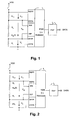
- Fig. 1 illustrates a measurement device according to a first embodiment of the present invention, and arranged to obtain a digital signal DATA representing a temperature measured by a three-terminal temperature-sensitive resistance R H (T). Three-terminal temperature-sensitive resistances are most often used in temperature sensors.
- the part of the measurement device indicated with I1 is a three-port analog-to-digital converter suitable for calculating V A - V B V C , V A , V B and V C being signals at the input ports of the three-port analog-to-digital converter.
- Any analog-to-digital converter making use of samples can be used, for example a sigma-delta converter, a pipeline converter or a successive approximation converter.
- a three-port sigma-delta analog-to-digital converter can for example be prepared in an easy way to do this.
- This analog-to-digital converter has an input port comprising a positive input terminal INP and a negative input terminal INN, a reference port comprising a positive reference terminal REFP and a negative reference terminal REFN, and an offset port comprising a positive offset terminal OFFP and a negative offset terminal OFFN.
- the three-port analog-to-digital converter for example the sigma-delta converter, may be of a well known conventional design.
- a differential signal input V 23 is applied between the input terminals INP and INN.
- a differential reference voltage input signal V 12 is applied between the reference terminals REFP and REFN.
- a differential offset voltage input signal is applied between the offset terminals OFFP and OFFN.
- a reference element for example a precise reference resistor R SH , such as e.g. RN-776-476 obtainable from MultiComp 8E160D-341-897 obtainable from Philips or RCC55 obtainable from Welwyn for example, may be connected between the reference terminals REFP and REFN.
- a sensing element for example a temperature-dependent resistor R H (T), such as e.g. PT100 obtainable from Calibration, ElAxxxx obtainable from Siemens, Germany or YGAxxxTB obtainable from Philips, Holland for example, may be connected between the input terminals INP and INN.
- An element emulating a parasitic value of the sensing element R H (T), for example a parasitic contact resistance R L of the sensing element, may be connected between the offset terminals OFFP and OFFN. There is counted on the fact that the parasitic contact resistance R L of the sensing element R H (T) is measured at one side, which is possible in view of the third terminal of the sensing resistor, and is subtracted from the other side.
- Eq. (1) is directly processed during one integration or conversion cycle. Instead of a standard sequence of three voltage measurement conversion cycles using a reference voltage, only one cycle is used and no reference voltage is involved.
- the output of the sigma-delta analog-to-digital converter I1 is a pulse density modulated signal PDM.
- This signal PDM is applied to a digital signal processing (DSP) block I2.
- DSP digital signal processing
- This block is suitable for processing the input PDM signal to an output digital word DATA.
- This digital word DATA carries the indirect temperature information.
- Fig. 2 illustrates a measurement device according to a second embodiment of the present invention, and arranged to obtain a digital signal DATA representing a temperature measured by a two-terminal temperature-sensitive resistance R H (T).
- the part of the measurement device indicated with I1 is a three-port analog-to-digital converter suitable for calculating V A - V B V C , V A , V B and V C being signals at the input ports of the three-port analog-to-digital converter.
- any three-port analog-to-digital converter making use of samples can be used.
- the three-port analog-to-digital converter may be of a conventional design.
- the analog-to-digital converter used has an input port comprising a positive input terminal INP and a negative input terminal INN, a reference port comprising a positive reference terminal REFP and a negative reference terminal REFN, and an offset port comprising a positive offset terminal OFFP and a negative offset terminal OFFN.
- a differential signal input V 23 is applied between the input terminals INP and INN.
- a differential reference voltage input signal V 12 is applied between the reference terminals REFP and REFN.
- a differential offset voltage input signal is applied between the offset terminals OFFP and OFFN.
- a reference element for example a precise reference resistor R SH , such as e.g. RN-776-476 obtainable from MultiComp, 8E160D-341-897 obtainable from Philips or RCC55 obtainable from Welwyn, may be connected between the reference terminals REFP and REFN.
- a sensing element for example a temperature-dependent resistor R H (T), such as e.g. PT100 obtainable from Calibration, EIAxxxx obtainable from Siemens, Germany or YGAxxxTB obtainable from Philips, Holland for example, may be connected between the input terminals INP and INN.
- An element emulating a parasitic value of the sensing element R H (T) for example a resistor equal to twice a parasitic contact resistance R L of the sensing element, may be connected between the offset terminals OFFP and OFFN.
- Eq. (2) is obtained, which is equal to Eq. (1), and again this equation is directly processed during one integration or conversion cycle. Instead of a standard sequence of three voltage measurement conversion cycles using a reference voltage, only one cycle is used and no reference voltage is involved.
- the output of the sigma-delta analog-to-digital converter I1 is a pulse density modulated signal PDM.
- This signal PDM is applied to a digital signal processing (DSP) block I2.
- DSP digital signal processing
- This block is suitable for processing the input PDM signal to an output digital word DATA.
- This digital word DATA carries the indirect temperature information.
- a means for deriving a relationship between an input signal and the reference signal may be part of the analog-to-digital converter. From the relationship, a value relating to the physical value may be computed using a computation unit; either a dedicated computation means for deriving said value, or a general purpose computation means being programmed for deriving said value relating to the physical value.
- the dedicated computation means may be any suitable device such as a microprocessor or a programmable logic device (sometimes referred to as PAL, PLA, FPLA, PLD, EPLD, EEPLD, LCA or FPGA), which are well-known integrated circuits that provide the advantages of fixed integrated circuits with the flexibility of custom integrated circuits. Such devices allow a user to electrically program standard, off-the-shelf logic elements to meet a user's specific needs, in this case to derive, from the relationship, the value relating to the physical value.
- a limiting factor is the ratio V 23 - V 3 V 12 , which must be in the range of 0 to 1, e.g. typically 0.9 to achieve a required resolution e.g. of 12 bits for a sigma-delta analog-to-digital converter (mainly due to intrinsic sigma-delta signal to noise ratio characteristics).
Landscapes
- Engineering & Computer Science (AREA)
- Theoretical Computer Science (AREA)
- Physics & Mathematics (AREA)
- General Physics & Mathematics (AREA)
- Analogue/Digital Conversion (AREA)
- Measuring Temperature Or Quantity Of Heat (AREA)
Claims (14)
- Messverfahren zum Messen eines physikalischen Wertes, umfassend, während eines Umwandlungszyklus: Bilden eines Eingangssignals (V23), eines Referenzsignals (V12) und eines Offset-Signals (V3), wobei das Eingangssignal einen parasitären Wert und einen nützlichen Messwert enthält, wobei die Signale jeweils einem Eingangselement (RH), einem Referenzelement (RSH) beziehungsweise einem Element (RL), das einem parasitären Wert entspricht, zugeordnet sind,
dadurch gekennzeichnet, dass
alle Elemente entweder in Serie oder parallel gekoppelt sind und dass alle ein gemeinsames Ansteuersignal (VDD) eines selben Wertes haben, wobei der parasitäre Wert von dem gemeinsamen Ansteuersignal abhängig ist, und
ein Verhältnis zwischen dem Eingangssignal, aus dem der parasitäre Wert gelöscht wurde, und dem Referenzsignal abgeleitet wird, und
aus diesem Verhältnis ein Wert bestimmt wird, der sich auf den physikalischen Wert bezieht. - Messverfahren nach Anspruch 1, wobei das Eingangssignal eine erste Spannung (V23) ist.
- Messverfahren nach Anspruch 2, wobei die erste Spannung aus einem Gleichspannungsabfall über dem Erfassungselement (RH) erhalten wird.
- Messverfahren nach einem der vorangehenden Ansprüche, wobei das Referenzsignal eine zweite Spannung (V12) ist.
- Messverfahren nach Anspruch 4, wobei die zweite Spannung aus einem Gleichspannungsabfall über dem Referenzelement (RSH) erhalten wird.
- Messverfahren nach einem der vorangehenden Ansprüche, wobei das Referenzelement ein Referenzwiderstand ist.
- Messverfahren nach einem der vorangehenden Ansprüche, wobei das Offset-Signal eine dritte Spannung (V3) ist.
- Messverfahren nach Anspruch 7, wobei die dritte Spannung aus einem Gleichspannungsabfall über dem parasitären Element (RL) erhalten wird.
- Messverfahren nach einem der vorangehenden Ansprüche, wobei der physikalische Wert eines von einer Temperatur, einem Druck, einer Lichtstärke, einer Position enthält.
- Messsystem für eine indirekte Messung eines physikalischen Wertes, umfassend einen Analog/Digital-Wandler (I1) mit mindestens einem ersten (INN, INP), einem zweiten (REFP, REFN) und einem dritten Anschluss (OFFP, OFFN), wobei jeder der mindestens drei Anschlüsse zum Empfangen eines Eingangssignals von einem Element geeignet ist, wobei der Analog/Digital-Wandler zum Auswerten des physikalischen Wertes in einem Umwandlungszyklus geeignet ist,
ein Erfassungselement (RH) mit einem vordefinierten charakteristischen Parameter, der sich auf den zu messenden physikalischen Wert bezieht, der an den ersten Anschluss (INN, INP) gekoppelt ist, um ein Eingangssignal (V23) an den ersten Anschluss anzulegen,
ein Referenzelement (RSH), das an den zweiten Anschluss zum Anlegen eines Referenzsignals an den zweiten Anschluss gekoppelt ist,
ein Element (RL), entsprechend einem parasitären Wert des Erfassungselements, das an den dritten Anschluss gekoppelt ist, um einen parasitären Wert des Erfassungselements an den dritten Anschluss anzulegen,
dadurch gekennzeichnet, dass
alle Elemente entweder in Serie oder parallel gekoppelt sind und dass alle ein gemeinsames Ansteuersignal eines selben Wertes haben,
Mittel zum Ableiten eines Verhältnisses zwischen dem Eingangssignal, aus dem der parasitäre Wert des Erfassungselements gelöscht wurde, und dem Referenzsignal, und
Mittel zum Ableiten eines Wertes aus dem Verhältnis, der sich auf den physikalischen Wert bezieht. - Messsystem nach Anspruch 10, wobei das Referenzelement in Serie mit dem Erfassungselement gekoppelt ist.
- Messsystem nach Anspruch 10 oder 11, wobei das Element, entsprechend einem parasitären Wert des Erfassungselements, in Serie mit dem Erfassungselement gekoppelt ist.
- Messsystem nach einem der Ansprüche 10 bis 12, wobei das Referenzelement einen Referenzwiderstand umfasst.
- Messsystem nach einem der Ansprüche 10 bis 13, wobei der physikalische Wert eines von einer Temperatur, einem Druck, einer Lichtstärke, einer Position ist.
Priority Applications (3)
| Application Number | Priority Date | Filing Date | Title |
|---|---|---|---|
| DE60330112T DE60330112D1 (de) | 2003-03-28 | 2003-03-28 | Verfahren und Vorrichtung zur indirekten Messung einer physikalischen Grösse |
| EP03447069A EP1463205B8 (de) | 2003-03-28 | 2003-03-28 | Verfahren und Vorrichtung zur indirekten Messung einer physikalischen Grösse |
| US10/810,340 US7091725B2 (en) | 2003-03-28 | 2004-03-26 | Fast, high-resolution, indirect measurement of a physical value |
Applications Claiming Priority (1)
| Application Number | Priority Date | Filing Date | Title |
|---|---|---|---|
| EP03447069A EP1463205B8 (de) | 2003-03-28 | 2003-03-28 | Verfahren und Vorrichtung zur indirekten Messung einer physikalischen Grösse |
Publications (3)
| Publication Number | Publication Date |
|---|---|
| EP1463205A1 EP1463205A1 (de) | 2004-09-29 |
| EP1463205B1 true EP1463205B1 (de) | 2009-11-18 |
| EP1463205B8 EP1463205B8 (de) | 2010-05-26 |
Family
ID=32799246
Family Applications (1)
| Application Number | Title | Priority Date | Filing Date |
|---|---|---|---|
| EP03447069A Expired - Lifetime EP1463205B8 (de) | 2003-03-28 | 2003-03-28 | Verfahren und Vorrichtung zur indirekten Messung einer physikalischen Grösse |
Country Status (3)
| Country | Link |
|---|---|
| US (1) | US7091725B2 (de) |
| EP (1) | EP1463205B8 (de) |
| DE (1) | DE60330112D1 (de) |
Cited By (1)
| Publication number | Priority date | Publication date | Assignee | Title |
|---|---|---|---|---|
| DE102012212978B3 (de) * | 2012-07-24 | 2013-08-22 | Siemens Aktiengesellschaft | Prozessmessgerät |
Families Citing this family (1)
| Publication number | Priority date | Publication date | Assignee | Title |
|---|---|---|---|---|
| TWI350498B (en) * | 2006-03-21 | 2011-10-11 | Himax Tech Ltd | Overdriving value generating apparatus and method |
Family Cites Families (9)
| Publication number | Priority date | Publication date | Assignee | Title |
|---|---|---|---|---|
| JPS5648835B2 (de) * | 1972-11-15 | 1981-11-18 | ||
| US4217543A (en) * | 1977-05-23 | 1980-08-12 | John Fluke Mfg. Co., Inc. | Digital conductance meter |
| US5655305A (en) * | 1995-04-03 | 1997-08-12 | Fletcher; Taylor C. | High precision electronic digital thermometer |
| US5700090A (en) * | 1996-01-03 | 1997-12-23 | Rosemount Inc. | Temperature sensor transmitter with sensor sheath lead |
| US6140952A (en) * | 1997-12-26 | 2000-10-31 | Rosemount Inc. | Delta sigma circuit with pulse width modulated offset |
| DE69910591T2 (de) * | 1999-11-19 | 2004-06-24 | Ami Semiconductor Belgium Bvba | Wandlerschnittstellenanordnung mit einem Sigma-Delta-Modulator mit Nullpunktabgleich und Verstärkungseinstellung |
| JP4568982B2 (ja) * | 2000-10-06 | 2010-10-27 | 株式会社デンソー | 物理量検出装置 |
| US20020113586A1 (en) * | 2001-02-22 | 2002-08-22 | Ho Edward Shan-Wei | Method and apparatus for offset correction |
| US6870357B1 (en) * | 2002-11-21 | 2005-03-22 | National Semiconductor Corporation | Method and apparatus for determining the temperature of a junction using voltage responses of the junction and a correction factor |
-
2003
- 2003-03-28 DE DE60330112T patent/DE60330112D1/de not_active Expired - Lifetime
- 2003-03-28 EP EP03447069A patent/EP1463205B8/de not_active Expired - Lifetime
-
2004
- 2004-03-26 US US10/810,340 patent/US7091725B2/en not_active Expired - Lifetime
Cited By (1)
| Publication number | Priority date | Publication date | Assignee | Title |
|---|---|---|---|---|
| DE102012212978B3 (de) * | 2012-07-24 | 2013-08-22 | Siemens Aktiengesellschaft | Prozessmessgerät |
Also Published As
| Publication number | Publication date |
|---|---|
| EP1463205B8 (de) | 2010-05-26 |
| US7091725B2 (en) | 2006-08-15 |
| EP1463205A1 (de) | 2004-09-29 |
| US20040257091A1 (en) | 2004-12-23 |
| DE60330112D1 (de) | 2009-12-31 |
Similar Documents
| Publication | Publication Date | Title |
|---|---|---|
| US9157937B2 (en) | Capacitance to digital converter and method | |
| US4082998A (en) | Dual slope integration circuit | |
| US20050248351A1 (en) | Self-calibrating device for measuring voltage and corresponding method | |
| EP3022737B1 (de) | Strommessschaltung mit versatzkalibrierung | |
| JP2002296072A (ja) | 角度測定装置 | |
| CN111263889A (zh) | 用于运行电池传感器的方法和电池传感器 | |
| CN101943713B (zh) | 内部自检查电阻桥和方法 | |
| EP1922554B1 (de) | Strommessschaltung und verfahren zur fehlerdiagnose darin | |
| US6255976B1 (en) | Low-frequency noise removing method and a related CMOS sensing circuit | |
| KR100384355B1 (ko) | 부성온도계수센서를사용하여온도를측정하는방법및관련장치 | |
| US6529847B2 (en) | Multivariable transmitter | |
| EP0496147A1 (de) | Rauschunempfindliche, kalibrierte Messung niedriger Widerstände | |
| US6479986B1 (en) | Time/analog converter for a magnetostrictive position sensor | |
| EP1463205B1 (de) | Verfahren und Vorrichtung zur indirekten Messung einer physikalischen Grösse | |
| EP3324546A1 (de) | Widerstandssensor-frontendsystem mit sigma-delta-analog-digital-wandler | |
| DE3200353A1 (de) | Verfahren und schaltungsanordnung, insbesondere zur temperaturmessung | |
| EP1498741B1 (de) | Wattstundenzähler mit integriertem Selbsttest | |
| US5831427A (en) | Voltage measuring device for a source with unknown resistance | |
| JP3189866B2 (ja) | 抵抗計校正装置 | |
| SU1762245A1 (ru) | Способ электрических измерений с применением параметрического мостового преобразовател | |
| JPS61223622A (ja) | 多温度計測装置 | |
| JP3937364B2 (ja) | 電圧・抵抗発生測定装置 | |
| JPS6147368B2 (de) | ||
| KR0127228B1 (ko) | 자동판매기 온도센서의 출력 독취방법 | |
| CN117419823A (zh) | 温度采集电路和装置 |
Legal Events
| Date | Code | Title | Description |
|---|---|---|---|
| PUAI | Public reference made under article 153(3) epc to a published international application that has entered the european phase |
Free format text: ORIGINAL CODE: 0009012 |
|
| AK | Designated contracting states |
Kind code of ref document: A1 Designated state(s): AT BE BG CH CY CZ DE DK EE ES FI FR GB GR HU IE IT LI LU MC NL PT RO SE SI SK TR |
|
| AX | Request for extension of the european patent |
Extension state: AL LT LV MK RO |
|
| 17P | Request for examination filed |
Effective date: 20050303 |
|
| AKX | Designation fees paid |
Designated state(s): DE FR |
|
| 17Q | First examination report despatched |
Effective date: 20080404 |
|
| GRAP | Despatch of communication of intention to grant a patent |
Free format text: ORIGINAL CODE: EPIDOSNIGR1 |
|
| GRAS | Grant fee paid |
Free format text: ORIGINAL CODE: EPIDOSNIGR3 |
|
| GRAA | (expected) grant |
Free format text: ORIGINAL CODE: 0009210 |
|
| AK | Designated contracting states |
Kind code of ref document: B1 Designated state(s): DE FR |
|
| REF | Corresponds to: |
Ref document number: 60330112 Country of ref document: DE Date of ref document: 20091231 Kind code of ref document: P |
|
| RAP2 | Party data changed (patent owner data changed or rights of a patent transferred) |
Owner name: SEMICONDUCTOR COMPONENTS INDUSTRIES, LLC |
|
| PLBE | No opposition filed within time limit |
Free format text: ORIGINAL CODE: 0009261 |
|
| STAA | Information on the status of an ep patent application or granted ep patent |
Free format text: STATUS: NO OPPOSITION FILED WITHIN TIME LIMIT |
|
| 26N | No opposition filed |
Effective date: 20100819 |
|
| REG | Reference to a national code |
Ref country code: FR Ref legal event code: PLFP Year of fee payment: 14 |
|
| REG | Reference to a national code |
Ref country code: FR Ref legal event code: PLFP Year of fee payment: 15 |
|
| REG | Reference to a national code |
Ref country code: FR Ref legal event code: PLFP Year of fee payment: 16 |
|
| PGFP | Annual fee paid to national office [announced via postgrant information from national office to epo] |
Ref country code: DE Payment date: 20200218 Year of fee payment: 18 |
|
| PGFP | Annual fee paid to national office [announced via postgrant information from national office to epo] |
Ref country code: FR Payment date: 20200220 Year of fee payment: 18 |
|
| REG | Reference to a national code |
Ref country code: DE Ref legal event code: R119 Ref document number: 60330112 Country of ref document: DE |
|
| PG25 | Lapsed in a contracting state [announced via postgrant information from national office to epo] |
Ref country code: DE Free format text: LAPSE BECAUSE OF NON-PAYMENT OF DUE FEES Effective date: 20211001 Ref country code: FR Free format text: LAPSE BECAUSE OF NON-PAYMENT OF DUE FEES Effective date: 20210331 |