EP1463108A2 - Method for manufacturing buried insulating layer type single crystal silicon carbide substrate and manufacturing device for the same - Google Patents
Method for manufacturing buried insulating layer type single crystal silicon carbide substrate and manufacturing device for the same Download PDFInfo
- Publication number
- EP1463108A2 EP1463108A2 EP04251663A EP04251663A EP1463108A2 EP 1463108 A2 EP1463108 A2 EP 1463108A2 EP 04251663 A EP04251663 A EP 04251663A EP 04251663 A EP04251663 A EP 04251663A EP 1463108 A2 EP1463108 A2 EP 1463108A2
- Authority
- EP
- European Patent Office
- Prior art keywords
- silicon carbide
- thin film
- gas
- single crystal
- crystal silicon
- Prior art date
- Legal status (The legal status is an assumption and is not a legal conclusion. Google has not performed a legal analysis and makes no representation as to the accuracy of the status listed.)
- Withdrawn
Links
Images


Classifications
-
- H—ELECTRICITY
- H10—SEMICONDUCTOR DEVICES; ELECTRIC SOLID-STATE DEVICES NOT OTHERWISE PROVIDED FOR
- H10P—GENERIC PROCESSES OR APPARATUS FOR THE MANUFACTURE OR TREATMENT OF DEVICES COVERED BY CLASS H10
- H10P90/00—Preparation of wafers not covered by a single main group of this subclass, e.g. wafer reinforcement
- H10P90/19—Preparing inhomogeneous wafers
- H10P90/1904—Preparing vertically inhomogeneous wafers
- H10P90/1906—Preparing SOI wafers
-
- C—CHEMISTRY; METALLURGY
- C02—TREATMENT OF WATER, WASTE WATER, SEWAGE, OR SLUDGE
- C02F—TREATMENT OF WATER, WASTE WATER, SEWAGE, OR SLUDGE
- C02F1/00—Treatment of water, waste water, or sewage
- C02F1/28—Treatment of water, waste water, or sewage by sorption
- C02F1/283—Treatment of water, waste water, or sewage by sorption using coal, charred products, or inorganic mixtures containing them
-
- C—CHEMISTRY; METALLURGY
- C02—TREATMENT OF WATER, WASTE WATER, SEWAGE, OR SLUDGE
- C02F—TREATMENT OF WATER, WASTE WATER, SEWAGE, OR SLUDGE
- C02F1/00—Treatment of water, waste water, or sewage
- C02F1/44—Treatment of water, waste water, or sewage by dialysis, osmosis or reverse osmosis
-
- C—CHEMISTRY; METALLURGY
- C02—TREATMENT OF WATER, WASTE WATER, SEWAGE, OR SLUDGE
- C02F—TREATMENT OF WATER, WASTE WATER, SEWAGE, OR SLUDGE
- C02F1/00—Treatment of water, waste water, or sewage
- C02F1/50—Treatment of water, waste water, or sewage by addition or application of a germicide or by oligodynamic treatment
-
- C—CHEMISTRY; METALLURGY
- C23—COATING METALLIC MATERIAL; COATING MATERIAL WITH METALLIC MATERIAL; CHEMICAL SURFACE TREATMENT; DIFFUSION TREATMENT OF METALLIC MATERIAL; COATING BY VACUUM EVAPORATION, BY SPUTTERING, BY ION IMPLANTATION OR BY CHEMICAL VAPOUR DEPOSITION, IN GENERAL; INHIBITING CORROSION OF METALLIC MATERIAL OR INCRUSTATION IN GENERAL
- C23C—COATING METALLIC MATERIAL; COATING MATERIAL WITH METALLIC MATERIAL; SURFACE TREATMENT OF METALLIC MATERIAL BY DIFFUSION INTO THE SURFACE, BY CHEMICAL CONVERSION OR SUBSTITUTION; COATING BY VACUUM EVAPORATION, BY SPUTTERING, BY ION IMPLANTATION OR BY CHEMICAL VAPOUR DEPOSITION, IN GENERAL
- C23C16/00—Chemical coating by decomposition of gaseous compounds, without leaving reaction products of surface material in the coating, i.e. chemical vapour deposition [CVD] processes
- C23C16/02—Pretreatment of the material to be coated
- C23C16/0209—Pretreatment of the material to be coated by heating
- C23C16/0218—Pretreatment of the material to be coated by heating in a reactive atmosphere
-
- C—CHEMISTRY; METALLURGY
- C23—COATING METALLIC MATERIAL; COATING MATERIAL WITH METALLIC MATERIAL; CHEMICAL SURFACE TREATMENT; DIFFUSION TREATMENT OF METALLIC MATERIAL; COATING BY VACUUM EVAPORATION, BY SPUTTERING, BY ION IMPLANTATION OR BY CHEMICAL VAPOUR DEPOSITION, IN GENERAL; INHIBITING CORROSION OF METALLIC MATERIAL OR INCRUSTATION IN GENERAL
- C23C—COATING METALLIC MATERIAL; COATING MATERIAL WITH METALLIC MATERIAL; SURFACE TREATMENT OF METALLIC MATERIAL BY DIFFUSION INTO THE SURFACE, BY CHEMICAL CONVERSION OR SUBSTITUTION; COATING BY VACUUM EVAPORATION, BY SPUTTERING, BY ION IMPLANTATION OR BY CHEMICAL VAPOUR DEPOSITION, IN GENERAL
- C23C16/00—Chemical coating by decomposition of gaseous compounds, without leaving reaction products of surface material in the coating, i.e. chemical vapour deposition [CVD] processes
- C23C16/02—Pretreatment of the material to be coated
- C23C16/0227—Pretreatment of the material to be coated by cleaning or etching
- C23C16/0236—Pretreatment of the material to be coated by cleaning or etching by etching with a reactive gas
-
- C—CHEMISTRY; METALLURGY
- C23—COATING METALLIC MATERIAL; COATING MATERIAL WITH METALLIC MATERIAL; CHEMICAL SURFACE TREATMENT; DIFFUSION TREATMENT OF METALLIC MATERIAL; COATING BY VACUUM EVAPORATION, BY SPUTTERING, BY ION IMPLANTATION OR BY CHEMICAL VAPOUR DEPOSITION, IN GENERAL; INHIBITING CORROSION OF METALLIC MATERIAL OR INCRUSTATION IN GENERAL
- C23C—COATING METALLIC MATERIAL; COATING MATERIAL WITH METALLIC MATERIAL; SURFACE TREATMENT OF METALLIC MATERIAL BY DIFFUSION INTO THE SURFACE, BY CHEMICAL CONVERSION OR SUBSTITUTION; COATING BY VACUUM EVAPORATION, BY SPUTTERING, BY ION IMPLANTATION OR BY CHEMICAL VAPOUR DEPOSITION, IN GENERAL
- C23C16/00—Chemical coating by decomposition of gaseous compounds, without leaving reaction products of surface material in the coating, i.e. chemical vapour deposition [CVD] processes
- C23C16/22—Chemical coating by decomposition of gaseous compounds, without leaving reaction products of surface material in the coating, i.e. chemical vapour deposition [CVD] processes characterised by the deposition of inorganic material, other than metallic material
- C23C16/30—Deposition of compounds, mixtures or solid solutions, e.g. borides, carbides, nitrides
- C23C16/32—Carbides
- C23C16/325—Silicon carbide
-
- C—CHEMISTRY; METALLURGY
- C23—COATING METALLIC MATERIAL; COATING MATERIAL WITH METALLIC MATERIAL; CHEMICAL SURFACE TREATMENT; DIFFUSION TREATMENT OF METALLIC MATERIAL; COATING BY VACUUM EVAPORATION, BY SPUTTERING, BY ION IMPLANTATION OR BY CHEMICAL VAPOUR DEPOSITION, IN GENERAL; INHIBITING CORROSION OF METALLIC MATERIAL OR INCRUSTATION IN GENERAL
- C23C—COATING METALLIC MATERIAL; COATING MATERIAL WITH METALLIC MATERIAL; SURFACE TREATMENT OF METALLIC MATERIAL BY DIFFUSION INTO THE SURFACE, BY CHEMICAL CONVERSION OR SUBSTITUTION; COATING BY VACUUM EVAPORATION, BY SPUTTERING, BY ION IMPLANTATION OR BY CHEMICAL VAPOUR DEPOSITION, IN GENERAL
- C23C16/00—Chemical coating by decomposition of gaseous compounds, without leaving reaction products of surface material in the coating, i.e. chemical vapour deposition [CVD] processes
- C23C16/44—Chemical coating by decomposition of gaseous compounds, without leaving reaction products of surface material in the coating, i.e. chemical vapour deposition [CVD] processes characterised by the method of coating
- C23C16/48—Chemical coating by decomposition of gaseous compounds, without leaving reaction products of surface material in the coating, i.e. chemical vapour deposition [CVD] processes characterised by the method of coating by irradiation, e.g. photolysis, radiolysis, particle radiation
- C23C16/482—Chemical coating by decomposition of gaseous compounds, without leaving reaction products of surface material in the coating, i.e. chemical vapour deposition [CVD] processes characterised by the method of coating by irradiation, e.g. photolysis, radiolysis, particle radiation using incoherent light, UV to IR, e.g. lamps
-
- C—CHEMISTRY; METALLURGY
- C30—CRYSTAL GROWTH
- C30B—SINGLE-CRYSTAL GROWTH; UNIDIRECTIONAL SOLIDIFICATION OF EUTECTIC MATERIAL OR UNIDIRECTIONAL DEMIXING OF EUTECTOID MATERIAL; REFINING BY ZONE-MELTING OF MATERIAL; PRODUCTION OF A HOMOGENEOUS POLYCRYSTALLINE MATERIAL WITH DEFINED STRUCTURE; SINGLE CRYSTALS OR HOMOGENEOUS POLYCRYSTALLINE MATERIAL WITH DEFINED STRUCTURE; AFTER-TREATMENT OF SINGLE CRYSTALS OR A HOMOGENEOUS POLYCRYSTALLINE MATERIAL WITH DEFINED STRUCTURE; APPARATUS THEREFOR
- C30B1/00—Single-crystal growth directly from the solid state
- C30B1/10—Single-crystal growth directly from the solid state by solid state reactions or multi-phase diffusion
-
- C—CHEMISTRY; METALLURGY
- C30—CRYSTAL GROWTH
- C30B—SINGLE-CRYSTAL GROWTH; UNIDIRECTIONAL SOLIDIFICATION OF EUTECTIC MATERIAL OR UNIDIRECTIONAL DEMIXING OF EUTECTOID MATERIAL; REFINING BY ZONE-MELTING OF MATERIAL; PRODUCTION OF A HOMOGENEOUS POLYCRYSTALLINE MATERIAL WITH DEFINED STRUCTURE; SINGLE CRYSTALS OR HOMOGENEOUS POLYCRYSTALLINE MATERIAL WITH DEFINED STRUCTURE; AFTER-TREATMENT OF SINGLE CRYSTALS OR A HOMOGENEOUS POLYCRYSTALLINE MATERIAL WITH DEFINED STRUCTURE; APPARATUS THEREFOR
- C30B29/00—Single crystals or homogeneous polycrystalline material with defined structure characterised by the material or by their shape
- C30B29/10—Inorganic compounds or compositions
- C30B29/36—Carbides
-
- H—ELECTRICITY
- H10—SEMICONDUCTOR DEVICES; ELECTRIC SOLID-STATE DEVICES NOT OTHERWISE PROVIDED FOR
- H10D—INORGANIC ELECTRIC SEMICONDUCTOR DEVICES
- H10D62/00—Semiconductor bodies, or regions thereof, of devices having potential barriers
- H10D62/80—Semiconductor bodies, or regions thereof, of devices having potential barriers characterised by the materials
- H10D62/83—Semiconductor bodies, or regions thereof, of devices having potential barriers characterised by the materials being Group IV materials, e.g. B-doped Si or undoped Ge
- H10D62/832—Semiconductor bodies, or regions thereof, of devices having potential barriers characterised by the materials being Group IV materials, e.g. B-doped Si or undoped Ge being Group IV materials comprising two or more elements, e.g. SiGe
- H10D62/8325—Silicon carbide
-
- H—ELECTRICITY
- H10—SEMICONDUCTOR DEVICES; ELECTRIC SOLID-STATE DEVICES NOT OTHERWISE PROVIDED FOR
- H10P—GENERIC PROCESSES OR APPARATUS FOR THE MANUFACTURE OR TREATMENT OF DEVICES COVERED BY CLASS H10
- H10P90/00—Preparation of wafers not covered by a single main group of this subclass, e.g. wafer reinforcement
- H10P90/19—Preparing inhomogeneous wafers
- H10P90/1904—Preparing vertically inhomogeneous wafers
- H10P90/1906—Preparing SOI wafers
- H10P90/1914—Preparing SOI wafers using bonding
-
- H—ELECTRICITY
- H10—SEMICONDUCTOR DEVICES; ELECTRIC SOLID-STATE DEVICES NOT OTHERWISE PROVIDED FOR
- H10W—GENERIC PACKAGES, INTERCONNECTIONS, CONNECTORS OR OTHER CONSTRUCTIONAL DETAILS OF DEVICES COVERED BY CLASS H10
- H10W10/00—Isolation regions in semiconductor bodies between components of integrated devices
-
- H—ELECTRICITY
- H10—SEMICONDUCTOR DEVICES; ELECTRIC SOLID-STATE DEVICES NOT OTHERWISE PROVIDED FOR
- H10W—GENERIC PACKAGES, INTERCONNECTIONS, CONNECTORS OR OTHER CONSTRUCTIONAL DETAILS OF DEVICES COVERED BY CLASS H10
- H10W10/00—Isolation regions in semiconductor bodies between components of integrated devices
- H10W10/01—Manufacture or treatment
-
- H—ELECTRICITY
- H10—SEMICONDUCTOR DEVICES; ELECTRIC SOLID-STATE DEVICES NOT OTHERWISE PROVIDED FOR
- H10W—GENERIC PACKAGES, INTERCONNECTIONS, CONNECTORS OR OTHER CONSTRUCTIONAL DETAILS OF DEVICES COVERED BY CLASS H10
- H10W10/00—Isolation regions in semiconductor bodies between components of integrated devices
- H10W10/10—Isolation regions comprising dielectric materials
- H10W10/181—Semiconductor-on-insulator [SOI] isolation regions, e.g. buried oxide regions of SOI wafers
-
- H—ELECTRICITY
- H10—SEMICONDUCTOR DEVICES; ELECTRIC SOLID-STATE DEVICES NOT OTHERWISE PROVIDED FOR
- H10P—GENERIC PROCESSES OR APPARATUS FOR THE MANUFACTURE OR TREATMENT OF DEVICES COVERED BY CLASS H10
- H10P14/00—Formation of materials, e.g. in the shape of layers or pillars
- H10P14/20—Formation of materials, e.g. in the shape of layers or pillars of semiconductor materials
- H10P14/203—Formation of materials, e.g. in the shape of layers or pillars of semiconductor materials using transformation of metal, e.g. oxidation or nitridation
-
- H—ELECTRICITY
- H10—SEMICONDUCTOR DEVICES; ELECTRIC SOLID-STATE DEVICES NOT OTHERWISE PROVIDED FOR
- H10P—GENERIC PROCESSES OR APPARATUS FOR THE MANUFACTURE OR TREATMENT OF DEVICES COVERED BY CLASS H10
- H10P14/00—Formation of materials, e.g. in the shape of layers or pillars
- H10P14/20—Formation of materials, e.g. in the shape of layers or pillars of semiconductor materials
- H10P14/29—Formation of materials, e.g. in the shape of layers or pillars of semiconductor materials characterised by the substrates
- H10P14/2901—Materials
- H10P14/2902—Materials being Group IVA materials
- H10P14/2905—Silicon, silicon germanium or germanium
-
- H—ELECTRICITY
- H10—SEMICONDUCTOR DEVICES; ELECTRIC SOLID-STATE DEVICES NOT OTHERWISE PROVIDED FOR
- H10P—GENERIC PROCESSES OR APPARATUS FOR THE MANUFACTURE OR TREATMENT OF DEVICES COVERED BY CLASS H10
- H10P14/00—Formation of materials, e.g. in the shape of layers or pillars
- H10P14/20—Formation of materials, e.g. in the shape of layers or pillars of semiconductor materials
- H10P14/32—Formation of materials, e.g. in the shape of layers or pillars of semiconductor materials characterised by intermediate layers between substrates and deposited layers
- H10P14/3202—Materials thereof
- H10P14/3241—Materials thereof being conductive materials
-
- H—ELECTRICITY
- H10—SEMICONDUCTOR DEVICES; ELECTRIC SOLID-STATE DEVICES NOT OTHERWISE PROVIDED FOR
- H10P—GENERIC PROCESSES OR APPARATUS FOR THE MANUFACTURE OR TREATMENT OF DEVICES COVERED BY CLASS H10
- H10P14/00—Formation of materials, e.g. in the shape of layers or pillars
- H10P14/20—Formation of materials, e.g. in the shape of layers or pillars of semiconductor materials
- H10P14/34—Deposited materials, e.g. layers
- H10P14/3402—Deposited materials, e.g. layers characterised by the chemical composition
- H10P14/3404—Deposited materials, e.g. layers characterised by the chemical composition being Group IVA materials
- H10P14/3408—Silicon carbide
Definitions
- the present invention relates to a method for manufacturing a buried insulating layer type semiconductor silicon carbide substrate and a manufacturing device for the same. Concretely speaking, the present invention relates to a high performance silicon carbide substrate that has potential to be used as a next generation semiconductor substrate and that has an SOI structure allowing a low-loss, high-speed device.
- Manufacturing methods for manufacturing a buried insulating layer semiconductor silicon carbide substrate of this type include the step of heating the surface of an SOI substrate so that the surface silicon layer of this SOI substrate is metamorphosed to a single crystal silicon carbide thin film.
- the temperature of the entire stage for supporting an SOI substrate is raised (see Patent Literature 1) or the temperature of the entire atmosphere in the film formation chamber is raised.
- these heating systems for raising the temperature include a resistance heating system and an induction heating system.
- the entirety of the SOI substrate is heated. That is to say, a portion of the SOI substrate, which is not desired to be heated, is heated along with the surface silicon layer portion, which is required to be heated, and, therefore, the buried insulating layer directly beneath this surface silicon layer is softened or melted causing a lump of the surface silicon layer that has not been metamorphosed into a single crystal silicon carbide thin film to be buried into the buried insulating layer.
- a manufacturing method that includes the above described step has a problem, wherein, the flatness of the interface between the above-described single crystal silicon carbide thin film and the above-described buried insulating layer is deteriorated.
- the present invention is developed in view of the above-described situation, and an object thereof is to provide a method for manufacturing a buried insulating layer type semiconductor silicon carbide substrate that does not have the above-described problem, and a manufacturing device for the same.
- a method for manufacturing a buried insulating layer type semiconductor silicon carbide substrate comprises manufacturing a buried insulating layer type single crystal silicon carbide substrate within a film formation chamber after placing, in this film formation chamber, an SOI substrate having a buried insulating layer positioned on a silicon substrate and a surface silicon layer formed on this buried insulating layer, characterized by comprising: the first step of irradiating the surface silicon layer of the SOI substrate with infrared rays while supplying a mixed gas of hydrogen gas hydrocarbon gas into the film formation chamber and, thereby, raising the temperature of the surface silicon layer to that required for metamorphosing the surface silicon layer into a single crystal silicon carbide thin film wherein this condition is maintained for a predetermined period of time so that the surface silicon layer is metamorphosed into the single crystal silicon carbide thin film.
- the method may comprise further steps as follows: a second step of maintaining the same condition as of the above-described first step and, thereby, depositing a carbon thin film on the above-described single crystal silicon carbide thin film; a third step of replacing the above-described mixed gas with an inert gas mixed with oxygen gas with a predetermined ratio and at the same time adjusting the temperature of the above-described carbon thin film to that required for etching and removing the carbon thin film through the control of the irradiation of the infrared rays wherein this condition is maintained at a predetermined period of time so that the carbon thin film is etched and removed; and a fourth step of replacing the above-described inert gas with a pure inert gas with no oxygen gas mixed in and after that, adjusting the temperature of the above-described single crystal silicon carbide thin film to that required for making a new single crystal silicon carbide thin film grow on the above-described single crystal silicon carbide thin film through the control of the irradiation of the infrare
- a device for manufacturing a buried insulating layer type semiconductor silicon carbide substrate according to the present invention is a device for manufacturing a buried insulating layer type single crystal silicon carbide substrate within a film formation chamber after placing, in this film formation chamber, an SOI substrate having a buried insulating layer positioned on a silicon substrate and a surface silicon layer formed on this buried insulating layer, characterized by comprising: a film formation chamber in which the SOI substrate is placed; gas supplying means for supplying various types of gases required for the manufacture of the buried insulating layer type semiconductor silicon carbide substrate into the film formation chamber; infrared ray irradiating means for irradiating the surface silicon layer of the SOI substrate with infrared rays; and control means for controlling the gas supplying means and the infrared ray irradiating means, wherein the above-described control part irradiates the surface silicon layer of the SOI substrate with the infrared rays while supplying a mixed gas of hydrogen gas and
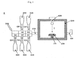
- Fig. 1 clarifies surrounding gases in the respective steps of the method for manufacturing a buried insulating layer type semiconductor silicon carbide substrate.
- measures of thickness of the respective layers in Fig. 3 are not proportionate to the actual thicknesses of the layers, for the convenience of the illustration.
- a manufacturing device A of a buried insulating layer type semiconductor silicon carbide substrate cited herein is a device for manufacturing a buried insulating layer type single crystal silicon carbide substrate within a film formation chamber 200 wherein, an SOI substrate 100 having a buried insulating layer 120 placed on a silicon substrate 110 and a surface silicon layer 130 formed on this buried insulating layer 120 is placed within the above-described film formation chamber 200 and is provided with: the film formation chamber 200 in which the SOI substrate 100 is placed; a gas supplying means 300 for supplying various types of gases required for the manufacturing of a buried insulating layer type semiconductor silicon carbide substrate to the film formation chamber 200; an infrared ray irradiating means 400 for irradiating the surface silicon layer 130 of the SOI substrate 100 with infrared rays I; and a control part 500 for controlling the gas supplying means 300 and the infrared ray irradiating means 400.
- each of the parts is described in detail.
- the SOI substrate 100 is an SIMOX (separation by Implanted Oxygen) substrate (see Fig. 3(a)).
- the film thickness of the surface silicon layer 130 of this SOI substrate is 10 nm or less and is concretely between 2 nm and 4 nm.
- SOI substrates 100 which are not SIMOX substrates.
- the film formation chamber 200 is formed of crystal or the like as shown in Fig. 1 and a stage 210 on which the SOI substrate 100 is placed is positioned inside the film formation chamber 200.
- This stage 210 is formed of crystal or ceramics.
- the types of crystal there are transparent crystal, opaque crystal, black crystal and the like having different absorptions of infrared rays, respectively. That is to say, different types of crystal are heated to different degrees by means of the infrared rays I.
- the quality of the crystal is selected appropriately in the case when crystal is used in the stage 210 taking into consideration the effects of the material to the temperature of the mounting surface of the SOI substrate 100.
- the SOI substrate 100 and the like are placed into and removed from the chamber through an entrance which is not shown.
- the infrared ray irradiating means 400 is attached to this film formation chamber 200 at a position opposite to the SOI substrate 100 placed on the stage 220.
- a pyrometer 700 (see Fig. 2) for measuring the inside temperature of the film formation chamber 200 is placed outside of the film formation chamber 200 so as to face the inside of the film formation chamber 200.
- the gas supplying means 300 for supplying various types of gases to the inside of the film formation chamber 200 and an exhaust means 600 for exhausting the above-described various types of gases are attached to the film formation chamber 200.
- the inside pressure of the film formation chamber 200 is set at a level equivalent to the atmospheric pressure.
- the gas supplying means 300 has a hydrogen gas supplying part 310 for supplying hydrogen gas G1, a hydrocarbon gas supplying part 320 for supplying hydrocarbon gas G2, an oxygen gas supplying part 330 for supplying oxygen gas G3, an inert gas supplying part 340 for supplying argon gas as inert gas G4 (including a pure inert gas) and a silane based gas supplying part 350 for supplying silane based gas G5.
- These gas supplying parts 310 to 350 are connected to switching valves 361 to 365 respectively and are connected to the film formation chamber 200 via a supplying pipe 370.
- an appropriate method for supplying a mixed gas is selected depending on the purpose.
- the hydrogen gas G1 is a carrier gas.
- Propane gas may be used as the hydrocarbon gas G2
- argon gas may be used as the inert gas G4
- monomethyl silane gas that includes silicon atoms and carbon atoms may be used as the silane based gas G5.
- dimethyl silane gas, trimethyl silane gas and the like, in addition to monmethyl silane gas, that include silicon atoms and carbon atoms can be utilized as the silane based gas G5.
- the infrared ray irradiating means 400 is a general infrared ray irradiating device for outputting infrared rays I having a wavelength of approximately 800 nm and the lamp part thereof is placed inside the film formation chamber 200.
- the wiring equipment of the infrared ray irradiating means 400 is positioned outside the film formation chamber 200.
- the infrared ray irradiating means 400 is formed in such a manner that the position thereof is adjustable. Concretely speaking, the infrared ray irradiating means 400 has a mechanism having an X-axis, a Y-axis and a rotational axis so that this mechanism is controlled by the control part 500.
- the position of the infrared ray irradiating means 400 is set in a manner that the entire surface of the surface silicon layer 130 of the SOI substrate 100 is irradiated with the infrared rays I.
- the position of the infrared ray irradiating means 400 can be adjusted so that the surface silicon layer 130 is metamorphosed locally to the single crystal silicon carbide thin film 140.
- the infrared ray irradiating means 400 may be able to output near and far infrared rays (of which the wavelength ranges from approximately 700 nm to 2500 nm).
- a sequencer is used as the control part 500 and the pyrometer 700 is electrically connected to the input port of the control part 500 while the switching valves 361 to 365, the switching valve of the exhaust means 600 and the infrared ray irradiating means 400 are electrically connected to the output port of the control part 500.
- the control part 500 is formed in a manner that an ON/OFF condition of each part is controlled based on a predetermined sequential pattern while inputting the measurement result of the pyrometer 700.
- control method of the control part 500 of the control device A and the method for manufacturing a buried insulating layer type semiconductor silicon carbide substrate using this control device A are described.
- the SOI substrate 100 is placed on the stage 210 within the film formation chamber 200.
- the switching valves 361 and 362 are switched and the hydrogen gas G1 is forced to eject from the hydrogen gas supplying part 310 at a rate of 1000 cc/minute and the hydrocarbon gas G2 is forced to eject from the hydrocarbon gas supplying part 320 at a rate of 10 cc/minute, respectively.
- a mixed gas G1 + G2
- the infrared ray irradiating means 400 is energized so that the surface silicon layer 130 of the SOI substrate 100 is irradiated with the infrared rays I.
- the temperature of the surface silicon layer 130 is raised to the temperature (approximately 1200°C) required for metamorphosing this surface silicon layer 130 into a single crystal silicon carbide thin film 140 so that this condition is maintained for 30 minutes and, thereby, this surface silicon layer 130 is metamorphosed into the single crystal silicon carbide thin film 140 (first step, see Fig. 3 (b)) .
- the temperature (approximately 1200°C) required for metamorphosing the surface silicon layer 130 of the SOI substrate 100 into the single crystal silicon carbide thin film 140 is gained solely by means of the infrared rays I and thus, the surface silicon layer 130 absorbs the infrared rays I so that the temperature thereof becomes approximately 1200°C.
- the buried insulating layer 120 absorbs almost no infrared rays I and the temperature thereof becomes of a value as low as approximately 250°C due to thermal conduction from the surface silicon layer 130 and the like.
- the temperature of the buried insulating layer 120 does not increase in the same manner as the surface silicon layer 130 unlike the prior art and this temperature stays at a level as low as approximately 250°C so as not to cause unnecessary changes such as melting or softening.
- the temperature required for metamorphosing the surface silicon layer 130 of the SOI substrate 100 into the single crystal silicon carbide thin film 140 may be in a range of from 500°C to 1450°C.
- the switching valves 363 and 364 are switched and the inert gas G4 is forced to eject from the inert gas supplying part 340 at a rate of 1000 cc/minute and the oxygen gas G3 is forced to eject from the oxygen gas supplying part 330 at a rate of 100 cc/minute, respectively.
- a mixed gas (G3 + G4) is supplied into the film formation chamber 200.
- the switching valve of the exhaust means 600 is opened for a predetermined period of time and, thereby, the mixed gas (G1 + G2) is exhausted to the outside of the film formation chamber 200.
- the mixed gas (G1 + G2) is replaced with the mixed gas (G3 + G4) in the above-described manner.
- the period of time for energizing the supplied power and the like of the infrared ray irradiating means 400 are controlled so that the temperature of the carbon thin film 150 is raised to the temperature (550°C or higher) required for etching and removing this carbon thin film 150 and this condition is maintained for 10 minutes and, thereby, this carbon thin film 150 is etched and removed (third step, see Fig. 3(d)).
- this carbon thin film 150 leads to a chemical change such as C + O ⁇ CO or C + O 2 ⁇ CO 2 , so that the carbon is changed into carbon monoxide gas or carbon dioxide gas. As a result, the carbon thin film 150 is etched and removed.
- the switching valve 364 is switched so that the inert gas G4 is forced to eject from the inert gas supplying part 340. As a result, the inert gas G4 is supplied into the film formation chamber 200.
- the switching valve of the exhaust means 600 is opened for a predetermined period of time and, thereby, the mixed gas (G3 + G4) is exhausted to the outside of the film formation chamber 200.
- the mixed gas (G3 + G4) is replaced with the above-described inert gas G4 in the above-described manner.
- the mixed gas (G3 + G4) is replaced with a pure inert gas G4 and, thereby, a risk of an explosive reaction between the oxygen gas G3 and the below described silane based gas can be avoided.
- the switching valves 361 and 365 are switched and the hydrogen gas G1 is forced to eject from the hydrogen gas supplying part 310 at a rate of 1000 cc/minute and the silane based gas G5 is forced to eject from the silane based gas supplying means 350 at a rate of 10 cc/minute, respectively.
- a mixed gas (G1 + G5) is supplied into the film formation chamber 200.
- the period of time of energizing the supplied power and the like of the infrared ray irradiating means 400 are controlled so as to achieve the temperature (approximately 1200°C) required for making a new single crystal silicon carbide thin film 160 grow on the single crystal silicon carbide thin film 140 and this condition is maintained for 30 minutes so that the new single crystal silicon carbide thin film 160 is made to grow on this single crystal silicon carbide thin film 140 (fourth step, see Fig. 3(e)).
- the silane based gas G5 is decomposed and causes a reaction on the single crystal silicon carbide thin film 140 in the above-described manner, and thereby another single crystal silicon carbide thin film 160 is formed on the single crystal silicon carbide thin film 140.
- the temperature required for making the new single crystal silicon carbide thin film 160 grown on the single crystal silicon carbide thin film 140 is in a range of from 500°C to 1450°C.
- a buried insulating layer type single crystal silicon carbide substrate having the single crystal silicon carbide thin films 140 and 160 is manufactured.
- the surface silicon layer 130 of the SOI substrate 100 is irradiated with the infrared rays I so that the temperature of surface silicon layer 130 is raised to that required for metamorphosing the surface silicon layer 130 into the single crystal silicon carbide thin film 140 solely by means of the infrared rays I and therefore, the temperature of the buried insulating layer 120 that absorbs almost no infrared rays I is not raised to a great amount.
- the buried insulating layer 120 can be prevented from being softened or melted and a lump of the surface silicon layer 130 that has not been metamorphosed into the single crystal silicon carbide thin film 140 can be prevented from being buried into this buried insulating layer 120 and as a result, a buried insulating layer type single crystal silicon carbide substrate having a high degree of flatness in the interface between the single crystal silicon carbide thin films 140, 160 and the buried insulating layer 120 can be gained.
- the position of the infrared ray irradiating means 400 was described as being adjustable, the structure thereof is not necessarily limited to such and the infrared ray irradiating means 400 may be fixed into the film formation chamber 200 so that the surface silicon layer 130 of the SOI substrate 100 is irradiated with the infrared rays I with an appropriate output level.
- the infrared ray irradiating means 400 may be provided outside the film formation chamber 200 in such a manner that its position can be adjusted.
- the film formation chamber 200 is formed of a transparent crystal.
- This transparent crystal absorbs almost no infrared rays and therefore, the surface silicon layer 130 of the SOI substrate 100 can be irradiated with the infrared rays I through walls of the film formation chamber 200.
- the temperature of the walls of this film formation chamber 200 does not increase preventing the occurrence of undesired decomposition of gases in the vicinity of these walls.
- the position of the infrared ray irradiating means 400 can be changed in the above-described manner, and therefore, the irradiated region, irradiating angle and the like can easily be adjusted before the first step for greater versatility in the same manner as in the above-described embodiment while the surface silicon layer 130 can be locally metamorphosed into the single crystal silicon carbide thin film 140.
- an electronically and optically fused device where an electronic device and an optic device are mixed on the same substrate can be manufactured when gallium nitride is deposited on this single crystal silicon carbide thin film 140 for the manufacture of the optical device.
- a gas gases mixed according to a predetermined ratio in the case of a mixed gas
- a gas gases mixed according to a predetermined ratio in the case of a mixed gas
- the type where various types of gases are separately supplied has a flexibility higher than that of the type where various types of gases mixed in advance according to a predetermined ratio are supplied regarding the point of view that the former type allows for an easy change of the mixture ratio of the various types of gases corresponding to a variety of chemical reactions.
- a mixture gas of the gas silane based gas G5 that includes silicon atoms and carbon atoms, as the silane based gas G5, and the hydrogen gas G1 is supplied in the above-described fourth step of the above-described manufacturing method
- monosilane gas, disilane gas, dichlorosilane gas or the like which includes silicon atoms but does not include carbon atoms may be used as the silane based gas G5 so that a mixture gas of such silane based gas G5, hydrogen gas G1 and hydrocarbon gas G2 may be supplied.
- a method for supplying for the mixed gas is selected in accordance with the purpose.
- a method for manufacturing a buried insulating layer type semiconductor silicon carbide substrate is a method for manufacturing a buried insulating layer type single crystal silicon carbide substrate within a film formation chamber after placing, in this film formation chamber, an SOI substrate having a buried insulating layer positioned on a silicon substrate and a surface silicon layer formed on this buried insulating layer, characterized by comprising a first step of irradiating the surface silicon layer of the SOI substrate with infrared rays while supplying a mixed gas of hydrogen gas and hydrocarbon gas into the film formation chamber and, thereby, raising the temperature of the surface silicon layer to that required for metamorphosing the surface silicon layer into a single crystal silicon carbide thin film wherein this condition is maintained for a predetermined period of time so as to metamorphose the surface silicon layer into the single crystal silicon carbide thin film.
- the surface silicon layer of the SOI substrate is irradiated with infrared rays so that the temperature of the surface silicon layer is raised to that required for metamorphosing the surface silicon layer to a single crystal silicon carbide thin film solely by means of the infrared rays and, therefore, the temperature of the buried insulating layer that absorbs almost no infrared rays is not raised greatly.
- the above-described buried insulating layer can be prevented from being softened or melted and a lump of the surface silicon layer that has not been metamorphosed into a single crystal silicon carbide thin film can be prevented from being buried into this buried insulating layer. Accordingly, a buried insulating layer type single crystal silicon carbide substrate having a high degree of flatness in the interface between the single crystal silicon carbide thin films and the buried insulating layer can be gained.
- a manufacturing device for a buried insulating layer type semiconductor silicon carbide substrate is a device for manufacturing a buried insulating layer type single crystal silicon carbide substrate within a film formation chamber after placing, in this film formation chamber, an SOI substrate having a buried insulating layer positioned on a silicon substrate and a surface silicon layer formed on this buried insulating layer, comprising: a film formation chamber in which an SOI substrate is placed; gas supplying means for supplying various types of gasses required for the manufacture of the buried insulating layer type semiconductor silicon carbide substrate into the film formation chamber; infrared ray irradiating means for irradiating the surface silicon layer of the SOI substrate with infrared rays; and control means for controlling the gas supplying means and the infrared ray irradiating means, wherein the above-described control part irradiates the surface silicon layer of the SOI substrate with the infrared rays while supplying a mixed gas of hydrogen gas and hydrocarbon gas
- an infrared ray irradiating means is used as a heating means in such a manufacturing device so that the temperature of the surface silicon layer of the SOI substrate is increased solely by means of infrared rays and, therefore, heat insulating equipment, and the like, involved in a resistance heating system or in an induction heating system together with the heater of the resistance heating system or the coil of the induction heating system become unnecessary unlike the prior art.
- a miniaturization of the device can be achieved to an extent greater than in the prior art.
Landscapes
- Chemical & Material Sciences (AREA)
- Engineering & Computer Science (AREA)
- Organic Chemistry (AREA)
- Materials Engineering (AREA)
- Metallurgy (AREA)
- Chemical Kinetics & Catalysis (AREA)
- Mechanical Engineering (AREA)
- General Chemical & Material Sciences (AREA)
- Inorganic Chemistry (AREA)
- Crystallography & Structural Chemistry (AREA)
- Life Sciences & Earth Sciences (AREA)
- Hydrology & Water Resources (AREA)
- Environmental & Geological Engineering (AREA)
- Water Supply & Treatment (AREA)
- Toxicology (AREA)
- Health & Medical Sciences (AREA)
- Recrystallisation Techniques (AREA)
- Chemical Vapour Deposition (AREA)
Abstract
Description
Claims (15)
- A method for manufacturing a buried insulating layer type semiconductor silicon carbide substrate within a film formation chamber after placing, in this film formation chamber, an SOI substrate having a buried insulating layer positioned on a silicon substrate and a surface silicon layer formed on this buried insulating layer, wherein the method for manufacturing a buried insulating layer type semiconductor silicon carbide substrate is characterized by comprising a first step of irradiating the surface silicon layer of the SOI substrate with infrared rays while supplying a mixed gas of hydrogen gas and hydrocarbon gas into the film formation chamber and, thereby, raising the temperature of the surface silicon layer to that required for metamorphosing the surface silicon layer into a single crystal silicon carbide thin film wherein this condition is maintained for a predetermined period of time so that the surface silicon layer is metamorphosed into a single crystal silicon carbide thin film.
- The method according to Claim 1, characterized by comprising:a second step of maintaining the same condition as of said first step for a predetermined period of time after said first step and, thereby, depositing a carbon thin film on said single crystal silicon carbide thin film; anda third step of replacing said mixed gas with an inert gas with oxygen gas mixed at a predetermined ratio and at the same time, achieving the temperature required for etching and removing said carbon thin film through the control of the irradiation of the infrared rays wherein this condition is maintained for a predetermined period of time so that the carbon thin film is etched and removed.
- The method according to Claim 2, characterized by comprising:a fourth step of replacing said inert gas with a pure inert gas with no oxygen gas mixed in after said third step and, after that, achieving the temperature required for making a new single crystal silicon carbide thin film to grow on said single crystal silicon carbide thin film through the control of the irradiation of the infrared rays while supplying a mixed gas of hydrogen gas and a silane based gas into the pure inert gas atmosphere wherein this condition is maintained for a predetermined period of time so that a new single crystal silicon carbide thin film is made to grow on the single crystal silicon carbide thin film.
- The method according to Claim 3, characterized in that said SOI substrate is a SIMOX substrate.
- The method according to Claim 3, characterized in that the film thickness of said surface silicon layer is 10 nm or less.
- The method according to Claim 3, characterized in that the pressure within the film formation chamber is set at atmospheric pressure.
- A device for manufacturing a buried insulating layer type single crystal silicon carbide substrate within a film formation chamber after placing, in this film formation chamber, an SOI substrate having a buried insulating layer positioned on a silicon substrate and a surface silicon layer formed on this buried insulating layer, wherein the manufacturing device for a buried insulating layer type silicon carbide substrate is characterized by comprising: a film formation chamber for receiving an SOI substrate; a gas supplying means for supplying various types of gases required for the manufacture of a buried insulating layer type semiconductor silicon carbide substrate into the film formation chamber; an infrared ray irradiating means for irradiating the surface silicon layer of the SOI substrate with infrared rays; and a control means for controlling the gas supplying means and the infrared ray irradiating means, wherein said control part irradiates the surface silicon layer of the SOI substrate with infrared rays while supplying a mixed gas of hydrogen gas and hydrocarbon gas into the film formation chamber, thereby raises the temperature of the surface silicon layer to that required for metamorphosing the surface silicon layer into a single crystal silicon carbide thin film, and maintains this condition for a predetermined period of time so that the surface silicon layer is metamorphosed into a single crystal silicon carbide thin film.
- The device according to Claim 7, characterized in that said control part continues the process for metamorphosing the surface silicon layer into a single crystal silicon carbide thin film for a predetermined period of time after the start of said process, thereby deposits a carbon thin film on said single crystal silicon carbide thin film and, after that, replaces said mixed gas with an inert gas mixed with oxygen gas at a predetermined ratio and at the same time, achieves a temperature required for etching and removing said carbon thin film through the control of the irradiation of the infrared rays, and maintains this condition for a predetermined period of time so that the carbon thin film is etched and removed.
- The device according to Claim 8, characterized in that said control part replaces said inert gas with a pure inert gas with no oxygen gas mixed in after the process for etching and removing said carbon thin film and, after that, achieves a temperature required for making a new single crystal silicon carbide thin film to grow on said single crystal silicon carbide thin film through the control of the irradiation of the infrared rays while supplying a mixed gas of hydrogen gas and a silane based gas into the pure inert gas atmosphere, and maintains this condition for a predetermined period of time so that a new single crystal silicon carbide thin film is made to grow on the single crystal silicon carbide thin film.
- The device according to Claim 9, characterized in that said SOI substrate is a SIMOX substrate.
- The device according to Claim 9, characterized in that the film thickness of said surface silicon layer is 10 nm or less.
- The device according to Claim 9, characterized in that the pressure within the film formation chamber is set at atmospheric pressure.
- The device according to Claim 9, characterized in that the position of said infrared ray irradiating means is adjustable.
- The device according to Claim 13, characterized in that said infrared ray irradiating means is placed outside a transparent film formation chamber.
- The device according to any one of claims 7 to 14, characterized by comprising a gas processing means for processing a gas supplied into said film formation chamber.
Priority Applications (1)
| Application Number | Priority Date | Filing Date | Title |
|---|---|---|---|
| EP07075382A EP1837904A3 (en) | 2003-03-26 | 2004-03-23 | Method for manufacturing buried insulating layer type single crystal silicon carbide substrate and corresponding manufacturing device |
Applications Claiming Priority (2)
| Application Number | Priority Date | Filing Date | Title |
|---|---|---|---|
| JP2003084056 | 2003-03-26 | ||
| JP2003084056A JP2004296558A (en) | 2003-03-26 | 2003-03-26 | Method and apparatus for manufacturing single crystal silicon carbide substrate with embedded insulating layer |
Related Child Applications (1)
| Application Number | Title | Priority Date | Filing Date |
|---|---|---|---|
| EP07075382A Division EP1837904A3 (en) | 2003-03-26 | 2004-03-23 | Method for manufacturing buried insulating layer type single crystal silicon carbide substrate and corresponding manufacturing device |
Publications (2)
| Publication Number | Publication Date |
|---|---|
| EP1463108A2 true EP1463108A2 (en) | 2004-09-29 |
| EP1463108A3 EP1463108A3 (en) | 2006-02-01 |
Family
ID=32821479
Family Applications (2)
| Application Number | Title | Priority Date | Filing Date |
|---|---|---|---|
| EP04251663A Withdrawn EP1463108A3 (en) | 2003-03-26 | 2004-03-23 | Method for manufacturing buried insulating layer type single crystal silicon carbide substrate and manufacturing device for the same |
| EP07075382A Withdrawn EP1837904A3 (en) | 2003-03-26 | 2004-03-23 | Method for manufacturing buried insulating layer type single crystal silicon carbide substrate and corresponding manufacturing device |
Family Applications After (1)
| Application Number | Title | Priority Date | Filing Date |
|---|---|---|---|
| EP07075382A Withdrawn EP1837904A3 (en) | 2003-03-26 | 2004-03-23 | Method for manufacturing buried insulating layer type single crystal silicon carbide substrate and corresponding manufacturing device |
Country Status (6)
| Country | Link |
|---|---|
| US (2) | US6927144B2 (en) |
| EP (2) | EP1463108A3 (en) |
| JP (1) | JP2004296558A (en) |
| KR (1) | KR20040084741A (en) |
| CN (1) | CN1324169C (en) |
| TW (1) | TW200421562A (en) |
Cited By (1)
| Publication number | Priority date | Publication date | Assignee | Title |
|---|---|---|---|---|
| CN116288253A (en) * | 2023-02-09 | 2023-06-23 | 浙江大学杭州国际科创中心 | Semiconductor film processing method, device, system and computer equipment |
Families Citing this family (9)
| Publication number | Priority date | Publication date | Assignee | Title |
|---|---|---|---|---|
| JP4563918B2 (en) * | 2005-10-31 | 2010-10-20 | エア・ウォーター株式会社 | Method for producing single crystal SiC substrate |
| JP5322044B2 (en) * | 2007-10-26 | 2013-10-23 | 国立大学法人九州工業大学 | Insulating layer embedded semiconductor silicon carbide substrate and method for manufacturing the same |
| JP5394632B2 (en) * | 2007-11-19 | 2014-01-22 | エア・ウォーター株式会社 | Method for producing single crystal SiC substrate |
| JP5151651B2 (en) * | 2008-04-22 | 2013-02-27 | 株式会社Sumco | Oxygen ion implanter |
| RU2425430C2 (en) * | 2009-12-31 | 2011-07-27 | Аслан Хаджимуратович Абдуев | Method to manufacture microinstrument |
| KR101355625B1 (en) * | 2012-10-15 | 2014-01-28 | 한국에너지기술연구원 | Apparatus for manufacturing silicon substrate and manufactring method of silicon substrate |
| JP6306411B2 (en) * | 2014-04-17 | 2018-04-04 | 株式会社日立国際電気 | Semiconductor device manufacturing method, substrate processing apparatus, and program |
| JP6732235B2 (en) * | 2014-12-02 | 2020-07-29 | 国立研究開発法人産業技術総合研究所 | Condensing mirror type heating furnace |
| CN115233308A (en) * | 2022-09-26 | 2022-10-25 | 青禾晶元(天津)半导体材料有限公司 | Silicon carbide crystal growth device and method |
Family Cites Families (16)
| Publication number | Priority date | Publication date | Assignee | Title |
|---|---|---|---|---|
| JPS60225434A (en) * | 1984-04-23 | 1985-11-09 | Nec Corp | Formation of multi-element composite oxide film with high dielectric constant |
| JPH0752305B2 (en) * | 1985-12-11 | 1995-06-05 | キヤノン株式会社 | Method for manufacturing electrophotographic photoreceptor |
| US5048163A (en) * | 1987-12-07 | 1991-09-17 | Asmus John F | System for processing semiconductor materials |
| JP2914992B2 (en) * | 1989-03-31 | 1999-07-05 | キヤノン株式会社 | Deposition film formation method |
| JP2962851B2 (en) * | 1990-04-26 | 1999-10-12 | キヤノン株式会社 | Light receiving member |
| ATE143703T1 (en) * | 1990-06-26 | 1996-10-15 | Air Liquide | METHOD FOR PRODUCING SELF-SUPPORTING MOLDED BODY FROM FIREPROOF METAL |
| US5436172A (en) * | 1991-05-20 | 1995-07-25 | Texas Instruments Incorporated | Real-time multi-zone semiconductor wafer temperature and process uniformity control system |
| US5424244A (en) * | 1992-03-26 | 1995-06-13 | Semiconductor Energy Laboratory Co., Ltd. | Process for laser processing and apparatus for use in the same |
| JPH06191997A (en) * | 1992-10-07 | 1994-07-12 | Kyushu Kogyo Univ | Method of forming SiC crystal film |
| US5759908A (en) * | 1995-05-16 | 1998-06-02 | University Of Cincinnati | Method for forming SiC-SOI structures |
| US5880491A (en) * | 1997-01-31 | 1999-03-09 | The United States Of America As Represented By The Secretary Of The Air Force | SiC/111-V-nitride heterostructures on SiC/SiO2 /Si for optoelectronic devices |
| TW476996B (en) * | 2000-02-28 | 2002-02-21 | Mitsubishi Material Silicon | Semiconductor manufacturing method and semiconductor manufacturing apparatus |
| WO2002000963A1 (en) * | 2000-06-23 | 2002-01-03 | Steven John Ouderkirk | Selective beam deposition |
| TW554405B (en) * | 2000-12-22 | 2003-09-21 | Seiko Epson Corp | Pattern generation method and apparatus |
| JP2002363751A (en) * | 2001-06-06 | 2002-12-18 | Osaka Prefecture | Method and apparatus for manufacturing single crystal silicon carbide thin film |
| US6566158B2 (en) * | 2001-08-17 | 2003-05-20 | Rosemount Aerospace Inc. | Method of preparing a semiconductor using ion implantation in a SiC layer |
-
2003
- 2003-03-26 JP JP2003084056A patent/JP2004296558A/en active Pending
-
2004
- 2004-03-01 TW TW093105310A patent/TW200421562A/en unknown
- 2004-03-12 US US10/708,593 patent/US6927144B2/en not_active Expired - Fee Related
- 2004-03-23 EP EP04251663A patent/EP1463108A3/en not_active Withdrawn
- 2004-03-23 EP EP07075382A patent/EP1837904A3/en not_active Withdrawn
- 2004-03-24 KR KR1020040019853A patent/KR20040084741A/en not_active Withdrawn
- 2004-03-26 CN CNB200410032250XA patent/CN1324169C/en not_active Expired - Fee Related
-
2005
- 2005-02-07 US US11/050,683 patent/US7077875B2/en not_active Expired - Fee Related
Cited By (1)
| Publication number | Priority date | Publication date | Assignee | Title |
|---|---|---|---|---|
| CN116288253A (en) * | 2023-02-09 | 2023-06-23 | 浙江大学杭州国际科创中心 | Semiconductor film processing method, device, system and computer equipment |
Also Published As
| Publication number | Publication date |
|---|---|
| JP2004296558A (en) | 2004-10-21 |
| CN1324169C (en) | 2007-07-04 |
| TW200421562A (en) | 2004-10-16 |
| EP1463108A3 (en) | 2006-02-01 |
| EP1837904A2 (en) | 2007-09-26 |
| KR20040084741A (en) | 2004-10-06 |
| CN1537979A (en) | 2004-10-20 |
| US7077875B2 (en) | 2006-07-18 |
| US20050136611A1 (en) | 2005-06-23 |
| EP1837904A3 (en) | 2007-12-26 |
| US20040191966A1 (en) | 2004-09-30 |
| US6927144B2 (en) | 2005-08-09 |
Similar Documents
| Publication | Publication Date | Title |
|---|---|---|
| US6774040B2 (en) | Apparatus and method for surface finishing a silicon film | |
| US6562720B2 (en) | Apparatus and method for surface finishing a silicon film | |
| US20230038611A1 (en) | Uv cure for local stress modulation | |
| US20130025538A1 (en) | Methods and apparatus for deposition processes | |
| JP3393469B2 (en) | Thin film semiconductor device manufacturing method and thin film semiconductor forming apparatus | |
| US7128788B2 (en) | Manufacturing apparatus for buried insulating layer-type semiconductor silicon carbide substrate | |
| US6927144B2 (en) | Method for manufacturing buried insulating layer type single crystal silicon carbide substrate | |
| JP2004533722A (en) | Doped silicon deposition process in a resistively heated single wafer chamber | |
| US7091138B2 (en) | Forming method and a forming apparatus of nanocrystalline silicon structure | |
| US7988835B2 (en) | Silicon dot forming method and silicon dot forming apparatus | |
| US20070158182A1 (en) | Silicon dot forming method and apparatus | |
| JP2010103495A (en) | Semiconductor device, and apparatus and method for manufacturing the same | |
| JP2564482B2 (en) | Deposition film forming equipment | |
| US7211514B2 (en) | Heat-processing method for semiconductor process under a vacuum pressure | |
| KR20050107510A (en) | Epitaxial semiconductor deposition methods and structrures | |
| KR20010053459A (en) | Method and apparatus for forming amorphous and polycrystalline silicon germanium alloy films | |
| JP3084395B2 (en) | Semiconductor thin film deposition method | |
| JPH0587171B2 (en) | ||
| US20230392255A1 (en) | Multiple Chamber System for Plasma Chemical Vapor Deposition of Diamond and Related Materials | |
| KR900001237B1 (en) | Manufacturing Method of Semiconductor Device | |
| JP2008028405A (en) | Semiconductor thin-film reforming apparatus | |
| WO2025126879A1 (en) | Substrate processing method, substrate processing device, and substrate processing system | |
| JPWO2007032053A1 (en) | Reaction gas supply apparatus and semiconductor manufacturing apparatus | |
| JPH06260423A (en) | Polysilicon film formation method | |
| JPH02238620A (en) | Selective growth of silicon film |
Legal Events
| Date | Code | Title | Description |
|---|---|---|---|
| PUAI | Public reference made under article 153(3) epc to a published international application that has entered the european phase |
Free format text: ORIGINAL CODE: 0009012 |
|
| AK | Designated contracting states |
Kind code of ref document: A2 Designated state(s): AT BE BG CH CY CZ DE DK EE ES FI FR GB GR HU IE IT LI LU MC NL PL PT RO SE SI SK TR |
|
| AX | Request for extension of the european patent |
Extension state: AL HR LT LV MK |
|
| PUAL | Search report despatched |
Free format text: ORIGINAL CODE: 0009013 |
|
| AK | Designated contracting states |
Kind code of ref document: A3 Designated state(s): AT BE BG CH CY CZ DE DK EE ES FI FR GB GR HU IE IT LI LU MC NL PL PT RO SE SI SK TR |
|
| AX | Request for extension of the european patent |
Extension state: AL LT LV MK |
|
| RIC1 | Information provided on ipc code assigned before grant |
Ipc: C23C 16/02 20060101ALI20051212BHEP Ipc: C23C 16/32 20060101ALI20051212BHEP Ipc: H01L 21/324 20060101ALI20051212BHEP Ipc: C30B 29/36 20060101ALI20051212BHEP Ipc: H01L 21/20 20060101ALI20051212BHEP Ipc: H01L 21/762 20060101AFI20040809BHEP |
|
| 17P | Request for examination filed |
Effective date: 20060220 |
|
| AKX | Designation fees paid |
Designated state(s): DE FR GB NL |
|
| 17Q | First examination report despatched |
Effective date: 20070102 |
|
| STAA | Information on the status of an ep patent application or granted ep patent |
Free format text: STATUS: THE APPLICATION IS DEEMED TO BE WITHDRAWN |
|
| 18D | Application deemed to be withdrawn |
Effective date: 20080607 |