EP1463102A2 - Procédé de fabrication d'un transistor à grille métallique, et transistor correspondant - Google Patents
Procédé de fabrication d'un transistor à grille métallique, et transistor correspondant Download PDFInfo
- Publication number
- EP1463102A2 EP1463102A2 EP04290693A EP04290693A EP1463102A2 EP 1463102 A2 EP1463102 A2 EP 1463102A2 EP 04290693 A EP04290693 A EP 04290693A EP 04290693 A EP04290693 A EP 04290693A EP 1463102 A2 EP1463102 A2 EP 1463102A2
- Authority
- EP
- European Patent Office
- Prior art keywords
- metal
- silicide
- process according
- metal silicide
- drain
- Prior art date
- Legal status (The legal status is an assumption and is not a legal conclusion. Google has not performed a legal analysis and makes no representation as to the accuracy of the status listed.)
- Withdrawn
Links
Images




Classifications
-
- H—ELECTRICITY
- H10—SEMICONDUCTOR DEVICES; ELECTRIC SOLID-STATE DEVICES NOT OTHERWISE PROVIDED FOR
- H10D—INORGANIC ELECTRIC SEMICONDUCTOR DEVICES
- H10D30/00—Field-effect transistors [FET]
- H10D30/01—Manufacture or treatment
- H10D30/021—Manufacture or treatment of FETs having insulated gates [IGFET]
- H10D30/0212—Manufacture or treatment of FETs having insulated gates [IGFET] using self-aligned silicidation
- H10D30/0213—Manufacture or treatment of FETs having insulated gates [IGFET] using self-aligned silicidation providing different silicide thicknesses on gate electrodes and on source regions or drain regions
-
- H—ELECTRICITY
- H10—SEMICONDUCTOR DEVICES; ELECTRIC SOLID-STATE DEVICES NOT OTHERWISE PROVIDED FOR
- H10D—INORGANIC ELECTRIC SEMICONDUCTOR DEVICES
- H10D64/00—Electrodes of devices having potential barriers
- H10D64/01—Manufacture or treatment
- H10D64/013—Manufacture or treatment of electrodes having a conductor capacitively coupled to a semiconductor by an insulator
- H10D64/01302—Manufacture or treatment of electrodes having a conductor capacitively coupled to a semiconductor by an insulator the insulator being formed after the semiconductor body, the semiconductor being silicon
- H10D64/01304—Manufacture or treatment of electrodes having a conductor capacitively coupled to a semiconductor by an insulator the insulator being formed after the semiconductor body, the semiconductor being silicon characterised by the conductor
- H10D64/01318—Manufacture or treatment of electrodes having a conductor capacitively coupled to a semiconductor by an insulator the insulator being formed after the semiconductor body, the semiconductor being silicon characterised by the conductor the conductor comprising a layer of alloy material, compound material or organic material contacting the insulator, e.g. TiN
- H10D64/0132—Manufacture or treatment of electrodes having a conductor capacitively coupled to a semiconductor by an insulator the insulator being formed after the semiconductor body, the semiconductor being silicon characterised by the conductor the conductor comprising a layer of alloy material, compound material or organic material contacting the insulator, e.g. TiN the conductor being a metallic silicide
-
- H—ELECTRICITY
- H10—SEMICONDUCTOR DEVICES; ELECTRIC SOLID-STATE DEVICES NOT OTHERWISE PROVIDED FOR
- H10D—INORGANIC ELECTRIC SEMICONDUCTOR DEVICES
- H10D64/00—Electrodes of devices having potential barriers
- H10D64/01—Manufacture or treatment
- H10D64/013—Manufacture or treatment of electrodes having a conductor capacitively coupled to a semiconductor by an insulator
- H10D64/01302—Manufacture or treatment of electrodes having a conductor capacitively coupled to a semiconductor by an insulator the insulator being formed after the semiconductor body, the semiconductor being silicon
- H10D64/01304—Manufacture or treatment of electrodes having a conductor capacitively coupled to a semiconductor by an insulator the insulator being formed after the semiconductor body, the semiconductor being silicon characterised by the conductor
- H10D64/01326—Aspects related to lithography, isolation or planarisation of the conductor
-
- H—ELECTRICITY
- H10—SEMICONDUCTOR DEVICES; ELECTRIC SOLID-STATE DEVICES NOT OTHERWISE PROVIDED FOR
- H10D—INORGANIC ELECTRIC SEMICONDUCTOR DEVICES
- H10D64/00—Electrodes of devices having potential barriers
- H10D64/01—Manufacture or treatment
- H10D64/017—Manufacture or treatment using dummy gates in processes wherein at least parts of the final gates are self-aligned to the dummy gates, i.e. replacement gate processes
-
- H—ELECTRICITY
- H10—SEMICONDUCTOR DEVICES; ELECTRIC SOLID-STATE DEVICES NOT OTHERWISE PROVIDED FOR
- H10D—INORGANIC ELECTRIC SEMICONDUCTOR DEVICES
- H10D64/00—Electrodes of devices having potential barriers
- H10D64/60—Electrodes characterised by their materials
- H10D64/66—Electrodes having a conductor capacitively coupled to a semiconductor by an insulator, e.g. MIS electrodes
- H10D64/667—Electrodes having a conductor capacitively coupled to a semiconductor by an insulator, e.g. MIS electrodes the conductor comprising a layer of alloy material, compound material or organic material contacting the insulator, e.g. TiN workfunction layers
- H10D64/668—Electrodes having a conductor capacitively coupled to a semiconductor by an insulator, e.g. MIS electrodes the conductor comprising a layer of alloy material, compound material or organic material contacting the insulator, e.g. TiN workfunction layers the layer being a silicide, e.g. TiSi2
Definitions
- the invention relates to integrated circuits and more particularly the manufacture of metal gate transistors.
- Transistors Isolated Grid Field Effect Transistors (Transistors) MOS), in particular by decreasing the gate resistance, avoiding the grid depletion and boron diffusion problems, and increasing the threshold voltage of the transistor.
- Transistors Isolated Grid Field Effect Transistors
- the chemical mechanical polishing step is a delicate operation that introduces strong variations on the final height grids, and which has a low yield.
- the invention aims to remedy these drawbacks.
- the invention is particularly aimed at producing grids metal by total silicidation of the grid region, while avoiding too deeply siliciding the source and drain.
- the invention proposes a method of producing a grid metal of a transistor comprising a total silicidation of the grid region.
- This total silicidation of the gate region is for example decoupled from the silicidation of the source and drain regions.
- the invention avoids the use of a step of chemical-mechanical polishing by making it impossible to take over silicidation on the active zones (because the second metal does not react with the first metal silicide) and using a mask layer hard, which also makes it possible to decouple the silicidation of the zones active silicidation of the grid.
- the metal silicide or silicides formed the least resistive possible it is particularly advantageous to make the metal silicide or silicides formed the least resistive possible. Also, is it advantageous that the siliciding phase comprises an annealing end of the first metal silicide and the second metal silicide, to respectively form a first metal final silicide and a second final silicide of metal.
- the first metal and the second metal may be the same.
- the first metal and the second metal can be different.
- the first metal and the second metal can be chosen for example in the group formed by titanium (Ti), platinum (Pt), nickel (Ni), cobalt (Co).
- the hard mask it may be formed for example of titanium nitride or else an alloy of silicon and germanium (Si x Ge 1-x ).
- the formation of the first metal silicide comprises for example a deposit of the first metal on the drain and source regions, and a first initial annealing.
- the formation of the second metal silicide for example includes a deposit of the second metal on the region of grid and on the first metal silicide, and a second initial annealing.
- the source, drain, and grid regions contain silicon, one can choose cobalt as the first metal and as second metal.
- the first initial annealing and the second initial annealing are carried out for example at a temperature below 600 ° C. approximately, to form CoSi as the first silicide of metal and second metal silicide.
- the final annealing can be carried out at a temperature above about 650 ° C, so as to form CoSi 2 (less resistive than CoSi) as the first metal final silicide and the second final metal silicide.
- the subject of the invention is also an integrated circuit comprising at least one transistor obtained by the method as defined above.
- the reference 1 denotes a semiconductor substrate, for example silicon, this substrate being optionally a box incorporated within a silicon wafer.
- an oxide layer 2 which is going to be intended to form the gate oxide of the future transistor.
- the layer of polysilicon that will, as we go see it in the example below, be intended to be silicided for form the metal gate of the transistor, has a thickness of 1000 to 1500 AT.
- a layer of hard mask 4 for example formed of titanium nitride TiN, and having example a thickness of the order of 100 ⁇ .
- a layer is formed of silicon dioxide which, as will be seen below, will serve also hard mask when burning the grid.
- the resin mask 70 is also used to engrave the layer of polysilicon 6 and therefore leave a residue 60 of polysilicon.
- the remainder 50 of oxide will serve as a hard mask to engrave the rest of the grid, i.e., the polysilicon layer 3.
- FIG. 5 which comprises the gate polysilicon 30 surmounted by hard mask layer 40 in TiN, itself surmounted by the remainder 50 oxide.
- the layer hard mask 40 is protected from normal cleaning operations by the oxide layer 50 which encapsulates it.
- silicidation that is to say the formation of a metal silicide, is obtained from cobalt.
- FIG. 8 It is then deposited (FIG. 8), for example by a plasma deposit vapor phase (PVD deposition), a layer of cobalt 8 on the source, drain, and also on the hard mask layer 40.
- PVD deposition plasma deposit vapor phase
- the thickness of the layer 8 is determined by function of the metal silicide thickness that you want finally get on the source and drain regions, knowing that when cobalt is used, 1 ⁇ of cobalt gives 3.4 ⁇ of silicide.
- a first initial annealing typically at a temperature below 600 ° C, for example at a temperature of the order of 530 ° C.
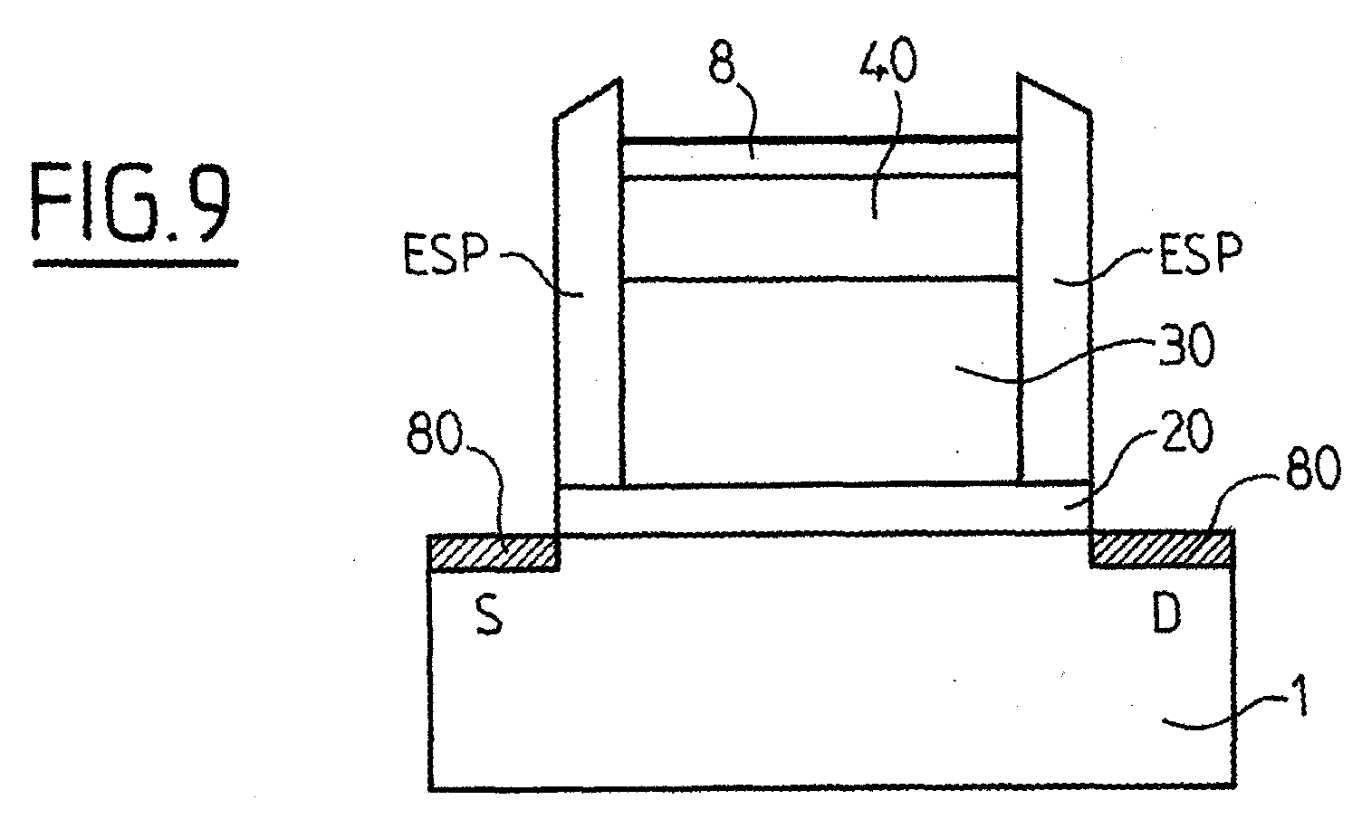
- Cobalt 8 then reacts with silicon from the source regions and drain, to form CoSi 80 ( Figure 9).
- cobalt 8 which was deposited on the mask layer 40, does not react with the polysilicon 30 of the grid, since it is protected by the hard mask layer 40.
- Unreacted cobalt i.e. cobalt which was on the hard mask layer 40, and optionally a cobalt residue unreacted with the silicon of the source and drain regions
- This selective removal operation is carried out for example by wet etching.
- Such wet etching is conventional and known per se, and it uses for example an NH 4 OH chemistry; H 2 O 2 ; H 2 O, or chemistry HCl, H 2 O 2 , H 2 O.
- This wet etching operation also etches the layer of Hard mask 40 made of titanium nitride (FIG. 10).
- a thick layer of cobalt 9 is then deposited on the structure of FIG. 10, the thickness of this layer of cobalt 9 being determined in order to silicide here the whole of the grid 30.
- a second initial annealing similar to first initial annealing, so as to react cobalt 9 with the polysilicon 30 of the grid and form CoSi 90 ( Figure 12).
- cobalt has the particularity of do not react with CoSi 80 from source and drain regions.
- CoSi is a highly resistive metal silicide, it is particularly advantageous in some applications to convert this CoSi to a much less resistive CoSi 2 .
- This transformation operation is carried out by proceeding to a final annealing, typically at a temperature above 650 ° C, by example around 830 ° C.
- the hard mask could also be formed of a silicon and germanium alloy.
- the invention is not limited to siliciding selective described above for the fabrication of a transistor, but proposes in a more general way, a siliciding process involving the formation of a metal silicide on two zones different semiconductors. These two different areas were in the example of the fabrication of a transistor described above, the regions source and drain on the one hand, and the gate region on the other hand
Landscapes
- Electrodes Of Semiconductors (AREA)
- Insulated Gate Type Field-Effect Transistor (AREA)
- Metal-Oxide And Bipolar Metal-Oxide Semiconductor Integrated Circuits (AREA)
Abstract
Description
- la formation à partir d'un premier métal, d'un premier siliciure de métal sur les régions de drain et de source, tandis que la région de grille est protégée par une couche de masque dur,
- le retrait du masque dur,
- la formation à partir d'un deuxième métal, d'un deuxième siliciure de métal dans la totalité de la région de grille de façon à siliciurer totalement la région de grille, tandis que le premier siliciure de métal est protégé par le deuxième métal ; et
- le retrait du deuxième métal.
- les figures 1 à 14 illustrent schématiquement les principales étapes d'un mode de mise en oeuvre du procédé selon l'invention, permettant d'aboutir à un transistor selon l'invention.
- la formation à partir d'un premier métal, d'un premier siliciure de métal sur une première zone, tandis que la deuxième zone est protégée par une couche de masque dur,
- le retrait du masque dur,
- la formation à partir d'un deuxième métal, d'un deuxième siliciure de métal sur la deuxième zone, tandis que le premier siliciure de métal est protégé par le deuxième métal ; et
- le retrait du deuxième métal.
Claims (14)
- Procédé de réalisation d'une grille métallique d'un transistor comprenant une siliciuration totale de la région de grille.
- Procédé selon la revendication 1, caractérisé par le fait que la phase de siliciuration comporte
la formation à partir d'un premier métal (8) d'un premier siliciure de métal (80) sur les régions de drain et de source tandis que la région de grille (30) est protégée par une couche de masque dur (40),
le retrait du masque dur,
la formation à partir d'un deuxième métal (9) d'un deuxième siliciure de métal (90) dans la totalité de la région de grille de façon à siliciurer totalement la région de grille, tandis que le premier siliciure de métal (80) est protégé par le deuxième métal (9), et
le retrait du deuxième métal (9). - Procédé selon la revendication 2, caractérisé par le fait que la phase de siliciuration comporte un recuit final du premier siliciure de métal et du deuxième siliciure de métal de façon à former respectivement un premier siliciure final de métal (100) et un deuxième siliciure final de métal (100).
- Procédé selon la revendication 2 ou 3, caractérisé par le fait que le premier métal (8) et le deuxième métal (9) sont identiques.
- Procédé selon la revendication 2 ou 3, caractérisé par le fait que le premier métal (8) et le deuxième métal (9) sont différents.
- Procédé selon l'une des revendications 2 à 5, caractérisé par le fait que le premier métal et le deuxième métal sont choisis dans le groupe formé par le titane (Ti), le platine (Pt), le nickel (Ni), le cobalt (Co).
- Procédé selon l'une des revendications 2 à 6, caractérisé par le fait que le masque dur (40) est formé de nitrure de titane (TiN) ou d'un alliage de silicium et de germanium (SixGe1-x).
- Procédé selon l'une des revendications 2 à 7, caractérisé par le fait que la formation du premier siliciure de métal comporte un dépôt du premier métal sur les régions de drain et de source, et un premier recuit initial.
- Procédé selon l'une des revendications 2 à 8 caractérisé par le fait que la formation du deuxième siliciure de métal comporte un dépôt du deuxième métal sur la région de grille et sur le premier siliciure de métal, et un deuxième recuit initial.
- Procédé selon l'une des revendications 2 à 9, caractérisé par le fait que les régions de source, de drain et de grille comportent du silicium et par le fait que le premier métal et le deuxième métal sont du cobalt.
- Procédé selon les revendications 8, 9 et 10, caractérisé par le fait que le premier recuit initial et le deuxième recuit initial sont effectués à une température inférieure à 600°C environ de façon à former du CoSi en tant que premier siliciure de métal (80) et deuxième siliciure de métal (90).
- Procédé selon les revendications 3 et 11, caractérisé par le fait que le recuit final est effectué à une température supérieure à 650°C environ, de façon à former du CoSi2 en tant que premier siliciure final de métal (100) et deuxième siliciure final de métal (100).
- Procédé selon l'une des revendications précédentes, caractérisé par le fait que la siliciuration totale de la région de grille est découplée de la siliciuration des régions de source et de drain.
- Circuit intégré comportant au moins un transistor obtenu par le procédé selon l'une des revendications 1 à 13.
Applications Claiming Priority (2)
| Application Number | Priority Date | Filing Date | Title |
|---|---|---|---|
| FR0303647 | 2003-03-25 | ||
| FR0303647A FR2853134B1 (fr) | 2003-03-25 | 2003-03-25 | Procede de fabrication d'un transistor a grille metallique, et transistor correspondant |
Publications (2)
| Publication Number | Publication Date |
|---|---|
| EP1463102A2 true EP1463102A2 (fr) | 2004-09-29 |
| EP1463102A3 EP1463102A3 (fr) | 2009-02-18 |
Family
ID=32799739
Family Applications (1)
| Application Number | Title | Priority Date | Filing Date |
|---|---|---|---|
| EP04290693A Withdrawn EP1463102A3 (fr) | 2003-03-25 | 2004-03-15 | Procédé de fabrication d'un transistor à grille métallique, et transistor correspondant |
Country Status (3)
| Country | Link |
|---|---|
| US (1) | US20050079695A1 (fr) |
| EP (1) | EP1463102A3 (fr) |
| FR (1) | FR2853134B1 (fr) |
Cited By (2)
| Publication number | Priority date | Publication date | Assignee | Title |
|---|---|---|---|---|
| WO2006103158A3 (fr) * | 2005-03-30 | 2006-12-07 | Infineon Technologies Ag | Schema d'integration pour une grille entierement recouverte d'une couche de siliciure |
| EP1744351A3 (fr) * | 2005-07-11 | 2008-11-26 | Interuniversitair Microelektronica Centrum ( Imec) | Procédé de fabrication d' un MOSFET ayant une porte entièrement silicidée et dispositifs obtenus |
Families Citing this family (9)
| Publication number | Priority date | Publication date | Assignee | Title |
|---|---|---|---|---|
| US7332421B2 (en) * | 2003-12-31 | 2008-02-19 | Dongbu Electronics Co., Ltd. | Method of fabricating gate electrode of semiconductor device |
| US7105889B2 (en) * | 2004-06-04 | 2006-09-12 | International Business Machines Corporation | Selective implementation of barrier layers to achieve threshold voltage control in CMOS device fabrication with high k dielectrics |
| US7271455B2 (en) * | 2004-07-14 | 2007-09-18 | International Business Machines Corporation | Formation of fully silicided metal gate using dual self-aligned silicide process |
| US7611943B2 (en) * | 2004-10-20 | 2009-11-03 | Texas Instruments Incorporated | Transistors, integrated circuits, systems, and processes of manufacture with improved work function modulation |
| US7229920B2 (en) * | 2005-01-11 | 2007-06-12 | United Microelectronics Corp. | Method of fabricating metal silicide layer |
| FR2881575B1 (fr) * | 2005-01-28 | 2007-06-01 | St Microelectronics Crolles 2 | Transistor mos a grille totalement siliciuree |
| EP1801858A1 (fr) * | 2005-12-23 | 2007-06-27 | INTERUNIVERSITAIR MICROELEKTRONICA CENTRUM vzw (IMEC) | Procédé de contrôle de hauteur d'une électrode à porte |
| US8652912B2 (en) * | 2006-12-08 | 2014-02-18 | Micron Technology, Inc. | Methods of fabricating a transistor gate including cobalt silicide |
| US11980046B2 (en) * | 2020-05-27 | 2024-05-07 | Taiwan Semiconductor Manufacturing Company, Ltd. | Method for forming an isolation structure having multiple thicknesses to mitigate damage to a display device |
Family Cites Families (6)
| Publication number | Priority date | Publication date | Assignee | Title |
|---|---|---|---|---|
| US5352631A (en) * | 1992-12-16 | 1994-10-04 | Motorola, Inc. | Method for forming a transistor having silicided regions |
| US6297135B1 (en) * | 1997-01-29 | 2001-10-02 | Ultratech Stepper, Inc. | Method for forming silicide regions on an integrated device |
| US6100173A (en) * | 1998-07-15 | 2000-08-08 | Advanced Micro Devices, Inc. | Forming a self-aligned silicide gate conductor to a greater thickness than junction silicide structures using a dual-salicidation process |
| US6153485A (en) * | 1998-11-09 | 2000-11-28 | Chartered Semiconductor Manufacturing Ltd. | Salicide formation on narrow poly lines by pulling back of spacer |
| US6271133B1 (en) * | 1999-04-12 | 2001-08-07 | Chartered Semiconductor Manufacturing Ltd. | Optimized Co/Ti-salicide scheme for shallow junction deep sub-micron device fabrication |
| US6228722B1 (en) * | 1999-04-16 | 2001-05-08 | United Microelectronics Corp. | Method for fabricating self-aligned metal silcide |
-
2003
- 2003-03-25 FR FR0303647A patent/FR2853134B1/fr not_active Expired - Fee Related
-
2004
- 2004-03-15 EP EP04290693A patent/EP1463102A3/fr not_active Withdrawn
- 2004-03-25 US US10/809,942 patent/US20050079695A1/en not_active Abandoned
Cited By (4)
| Publication number | Priority date | Publication date | Assignee | Title |
|---|---|---|---|---|
| WO2006103158A3 (fr) * | 2005-03-30 | 2006-12-07 | Infineon Technologies Ag | Schema d'integration pour une grille entierement recouverte d'une couche de siliciure |
| US7544553B2 (en) | 2005-03-30 | 2009-06-09 | Infineon Technologies Ag | Integration scheme for fully silicided gate |
| EP1744351A3 (fr) * | 2005-07-11 | 2008-11-26 | Interuniversitair Microelektronica Centrum ( Imec) | Procédé de fabrication d' un MOSFET ayant une porte entièrement silicidée et dispositifs obtenus |
| US7491635B2 (en) | 2005-07-11 | 2009-02-17 | Interuniversitair Microelektronica Centrum | Method for forming a fully silicided gate and devices obtained thereof |
Also Published As
| Publication number | Publication date |
|---|---|
| FR2853134B1 (fr) | 2005-07-01 |
| EP1463102A3 (fr) | 2009-02-18 |
| US20050079695A1 (en) | 2005-04-14 |
| FR2853134A1 (fr) | 2004-10-01 |
Similar Documents
| Publication | Publication Date | Title |
|---|---|---|
| EP2096676A1 (fr) | Procédé de fabrication d'un dispositif semi-conducteur à grille enterrée et circuit intégré correspondant. | |
| US6664154B1 (en) | Method of using amorphous carbon film as a sacrificial layer in replacement gate integration processes | |
| FR2804247A1 (fr) | Procede de realisation d'un transistor bipolaire a emetteur et base extrinseque auto-alignes | |
| EP0944919A1 (fr) | Transistor mis a grille metallique auto-alignee et son procede de fabrication | |
| FR2823010A1 (fr) | Procede de fabrication d'un transistor vertical a grille isolee a quadruple canal de conduction, et circuit integre comportant un tel transistor | |
| EP2045837B1 (fr) | Formation sélective d'un composé comprenant un matériau semi-conducteur et un matériau métallique dan un substrat, à travers une couche d'oxyde de germanium | |
| FR2853134A1 (fr) | Procede de fabrication d'un transistor a grille metallique, et transistor correspondant | |
| EP2120258B1 (fr) | Procédé de réalisation d'un transistor à source et drain métalliques | |
| EP1811549B1 (fr) | Procédé de retrait sélectif d'un métal non-siliciuré | |
| US11784090B2 (en) | Semiconductor structure | |
| FR3034254A1 (fr) | Procede de realisation d'un substrat de type soi, en particulier fdsoi, adapte a des transistors ayant des dielectriques de grilles d'epaisseurs differentes, substrat et circuit integre correspondants | |
| FR3000840A1 (fr) | Procede de realisation de contacts metalliques au sein d'un circuit integre, et circuit integre correspondant | |
| FR3082050A1 (fr) | Via interne avec contact ameliore pour couche semi-conductrice superieure d'un circuit 3d | |
| FR2750534A1 (fr) | Transistor et procede de realisation d'un transistor a contacts et a isolation de champ auto-alignes | |
| FR3037714A1 (fr) | Procede de realisation d'un contact sur une zone active d'un circuit integre, par exemple realise sur un substrat du type soi, en particulier fdsoi, et circuit integre correspondant | |
| FR2848726A1 (fr) | Transistor mis a grille auto-alignee et son procede de fabrication | |
| FR2947384A1 (fr) | Procede de realisation d'un transistor a source et drain metalliques | |
| EP3136429B1 (fr) | Formation de contacts ohmiques pour un dispositif dote d'une region en materiau iii-v et d'une region en un autre materiau semi-conducteur | |
| US8835292B2 (en) | Method of manufacturing semiconductor devices including replacement metal gate process incorporating a conductive dummy gate layer | |
| EP1627422B1 (fr) | Procede de delimitation d'un element conducteur dispose sur une couche isolante | |
| FR2856514A1 (fr) | Procede de formation selective de siliciure sur une plaque de materiau semi-conducteur | |
| US20160071954A1 (en) | Robust post-gate spacer processing and device | |
| FR3084773A1 (fr) | Procede de siliciuration de dispositif semiconducteur, et dispositif semiconducteur correspondant | |
| JPH11103053A (ja) | 半導体装置及びその製造方法 | |
| US20060166497A1 (en) | Method of fabricating conductive lines |
Legal Events
| Date | Code | Title | Description |
|---|---|---|---|
| PUAI | Public reference made under article 153(3) epc to a published international application that has entered the european phase |
Free format text: ORIGINAL CODE: 0009012 |
|
| AK | Designated contracting states |
Kind code of ref document: A2 Designated state(s): AT BE BG CH CY CZ DE DK EE ES FI FR GB GR HU IE IT LI LU MC NL PL PT RO SE SI SK TR |
|
| AX | Request for extension of the european patent |
Extension state: AL HR LT LV MK |
|
| RIN1 | Information on inventor provided before grant (corrected) |
Inventor name: TAVEL, BRICE Inventor name: SKOTNICKI, THOMAS Inventor name: CARRIERE, NICOLAS |
|
| 17P | Request for examination filed |
Effective date: 20050310 |
|
| PUAL | Search report despatched |
Free format text: ORIGINAL CODE: 0009013 |
|
| AK | Designated contracting states |
Kind code of ref document: A3 Designated state(s): AT BE BG CH CY CZ DE DK EE ES FI FR GB GR HU IE IT LI LU MC NL PL PT RO SE SI SK TR |
|
| AX | Request for extension of the european patent |
Extension state: AL LT LV MK |
|
| RIC1 | Information provided on ipc code assigned before grant |
Ipc: H01L 21/28 20060101ALI20090114BHEP Ipc: H01L 29/49 20060101ALI20090114BHEP Ipc: H01L 21/336 20060101AFI20040715BHEP |
|
| AKX | Designation fees paid |
Designated state(s): DE FR GB IT |
|
| STAA | Information on the status of an ep patent application or granted ep patent |
Free format text: STATUS: THE APPLICATION IS DEEMED TO BE WITHDRAWN |
|
| 18D | Application deemed to be withdrawn |
Effective date: 20090819 |