EP1460793A1 - Verfahren und Vorrichtung zur Fehlerzählung eines ausserhalb des Bereiches einer Augenmaske liegenden Datensignals - Google Patents
Verfahren und Vorrichtung zur Fehlerzählung eines ausserhalb des Bereiches einer Augenmaske liegenden Datensignals Download PDFInfo
- Publication number
- EP1460793A1 EP1460793A1 EP03006064A EP03006064A EP1460793A1 EP 1460793 A1 EP1460793 A1 EP 1460793A1 EP 03006064 A EP03006064 A EP 03006064A EP 03006064 A EP03006064 A EP 03006064A EP 1460793 A1 EP1460793 A1 EP 1460793A1
- Authority
- EP
- European Patent Office
- Prior art keywords
- eye
- recited
- threshold voltage
- data signal
- mask
- Prior art date
- Legal status (The legal status is an assumption and is not a legal conclusion. Google has not performed a legal analysis and makes no representation as to the accuracy of the status listed.)
- Withdrawn
Links
Images


Classifications
-
- G—PHYSICS
- G01—MEASURING; TESTING
- G01R—MEASURING ELECTRIC VARIABLES; MEASURING MAGNETIC VARIABLES
- G01R31/00—Arrangements for testing electric properties; Arrangements for locating electric faults; Arrangements for electrical testing characterised by what is being tested not provided for elsewhere
- G01R31/28—Testing of electronic circuits, e.g. by signal tracer
- G01R31/317—Testing of digital circuits
- G01R31/3181—Functional testing
- G01R31/319—Tester hardware, i.e. output processing circuits
- G01R31/3193—Tester hardware, i.e. output processing circuits with comparison between actual response and known fault free response
- G01R31/31937—Timing aspects, e.g. measuring propagation delay
-
- G—PHYSICS
- G01—MEASURING; TESTING
- G01R—MEASURING ELECTRIC VARIABLES; MEASURING MAGNETIC VARIABLES
- G01R31/00—Arrangements for testing electric properties; Arrangements for locating electric faults; Arrangements for electrical testing characterised by what is being tested not provided for elsewhere
- G01R31/28—Testing of electronic circuits, e.g. by signal tracer
- G01R31/317—Testing of digital circuits
- G01R31/31708—Analysis of signal quality
- G01R31/31711—Evaluation methods, e.g. shmoo plots
-
- H—ELECTRICITY
- H04—ELECTRIC COMMUNICATION TECHNIQUE
- H04L—TRANSMISSION OF DIGITAL INFORMATION, e.g. TELEGRAPHIC COMMUNICATION
- H04L1/00—Arrangements for detecting or preventing errors in the information received
- H04L1/20—Arrangements for detecting or preventing errors in the information received using signal quality detector
-
- H—ELECTRICITY
- H04—ELECTRIC COMMUNICATION TECHNIQUE
- H04L—TRANSMISSION OF DIGITAL INFORMATION, e.g. TELEGRAPHIC COMMUNICATION
- H04L1/00—Arrangements for detecting or preventing errors in the information received
- H04L1/24—Testing correct operation
- H04L1/242—Testing correct operation by comparing a transmitted test signal with a locally generated replica
-
- G—PHYSICS
- G01—MEASURING; TESTING
- G01R—MEASURING ELECTRIC VARIABLES; MEASURING MAGNETIC VARIABLES
- G01R13/00—Arrangements for displaying electric variables or waveforms
- G01R13/02—Arrangements for displaying electric variables or waveforms for displaying measured electric variables in digital form
Definitions
- This invention relates to systems that measure the performance of a high-speed data communications channel. More precisely, the preferred embodiment of the present invention is a method and apparatus for identifying a plurality of errors of a multi-valued data signal that occur outside the boundaries of an eye mask as defined by regions above, below and in the center of an eye diagram.
- bit error rate tester One approach of evaluating the performance of a high speed communications channel device or system is to use a bit error rate tester.
- a predetermined bit pattern is transmitted through the target channel, device or system and on to the bit error rate tester.
- the difference between the known transmitted bit pattern and the bit stream generated by the target device or system are considered errors and are accumulated by the bit error rate tester to determine the effective bit error rate (i.e., the fraction of the received or transmitted bits that are in error) of the target device or system.
- bit error rate testing BER is a relatively significant measure of performance, merely measuring the error rate of a high speed communications device or system does not provide enough data to characterize the behavior of a communications channel, device or system.
- instruments such as a bit error rate testers and oscilloscopes have the functionality of creating an eye diagram to facilitate characterizing a high-speed communications device or system during the various stages of development.
- a number of voltage levels of the data signal transmitted through a high-speed communications device or system is sampled at specified instances in time.
- a voltage-versus-time plot of errors known as "events" that depicts the behavior and performance of the high-speed communications component or subsystem is then generated and displayed as an eye diagram, for example.
- One technique of a more efficient way of validating the performance of a communications device or subsystem provides a quick indication of how a communications device or system performs against an industry develop characterization and performance template commonly referred to as an eye mask.
- These templates have been created by a number of industry groups to assure the interoperability of components or subsystems that might be configured into a number of different communication systems.
- a predetermined, known data signal is transmitted through the target device or subsystem to see the number of times the data signal that is generated by that device or subsystem deviates across the boundary of one or more of the zones as defined by the eye mask.
- the target device or subsystem If the data signal from the target device or subsystem does not deviate very many times into one or more of the zones, thereby producing only a limited number of mask violations, it is likely that the target device or subsystem will have little or no trouble operating properly and meeting or succeeding the specification of a particular application.
- bit error rate testing system There are several commercially available bit error rate testing system that characterize and validate the performance of a data signal from a device or communications subsystem using a form of an eye mask or template.
- Systems such as Agilent Technologies' 81250 as well as the 10G and the older 3G bit error rate testing systems measure the bit error rate of the data signal from a device or communications subsystem at various decision threshold levels and clock-to-data time delays in the eye diagram.
- the samples of the data signal transmitted through a target device or communications subsystem that are on the wrong side of a mask boundary for the center of the eye are displayed at different bit error rate levels then those that are on the correct side of the mask perimeter.
- Fig. 1 is a symmetric diagram of a typical bit error rate eye contour map produced by a prior art bit error rate testing systems.
- Fig. 1 shows the eye contour that comprises several different bit error rate levels where each level is represented by a different graphic icon.
- the outside contour 102 shown as a series of black circular icons designates a bit error rate of 10 4 or one error in 10,000 bits.
- This type of view of signal quality is accomplished by making a plurality of bit error rate measurements at various instances in time and voltage threshold. These measurements are then used, along with the theory for randomly distributed errors, to estimate the bit error rate at a given decision threshold by making bit error rate measurements at a series of decision thresholds and extrapolating to get an estimate the bit error rate of those areas that are not actually measured.
- the problem with this technique is that it may take minutes, if not hours, to complete depending on how "deep" a measurement is required. More importantly, these systems do not do an eye mask test but instead produce only a contour of the bit error rates of a data signal that has been transmitted through a target device or communications subsystem.
- the 81250 parallel bit error rate testing system measures the bit error rate at a specific number of points inside the opening of the eye in accordance with a supplied set of time-threshold voltage settings or parameters. This defines a set of extreme points or corners of the desired mask template and generates the results in a tabular spreadsheet-like format.
- the 81250 parallel bit error rate testing system calculates a partial mask violation report only about a polygon shaped area in the center of the eye diagram.
- the 81250 test system then employs up to 32 different locations inside the eye opening to form a polygon shaped template and then makes a series of quick bit error rate measurements at those locations. Even though the 81250 test system measures the bit error rate of the date signal for a finite number of points in the center of an eye diagram, it is not able to move the measuring point in areas above or below the eye diagram. As a result the 81250 test system can not measure the violations that might occur when a data signal from a target device or subsystem deviates across the boundaries and into the areas are either above or below the eye as specified by an industry standard eye mask. This is required to detect overshoot and undershoot or other signal quality degradations that manifest themselves above and/or below the eye center which does not necessarily effect the bit error rate of the transmitted signal but may effect other design limits of the device or system.
- An object of the present invention is to provide a method and apparatus for identifying a plurality of errors of a multi-valued data signal that occur outside the boundaries of an eye mask as defined by regions above, below or in the middle of the eye diagram, thus, overcoming at least some of the disadvantages and limitations of as implemented in the prior art.
- the method of measures the performance characteristics of an applied multi-valued data signals performed by a binary data bit decision mechanism that includes receiving program instructions to test for mask violations of the applied data signal produced for a particular bounded area; configuring variable delayed trigger to generate a plurality of trigger pulses equivalent to bit rate of the applied data signal; selecting appropriate bounded area; comparing the voltage level of the applied data signal with a supplied threshold voltage; comparing the comparative results with a supplied reference bit pattern accumulating mismatched events and transmitting the results to a program element or system.
- the invention will now be described illustrating a method and apparatus used to measure and display the number of time a multi-valued data signal transmitted from either a communication device of subsystem deviates across the boundaries and into one or more bounded areas or zones as defined by an eye mask that has been overlaid onto an eye diagram.
- the present invention employs an iterative process to accumulate and display mask violation that might result from a data signal transmitted from a target device or communications subsystem that deviates across the boundaries either above or below or into the center of the eye diagram.
- the present invention also has the ability to localize and isolate particular threshold voltage-delay points along the boundary lines above or below the eye diagram as well as around the perimeter of the mask polygon where mask violations have occurred so as to supply additional information and feedback about the behavior and performance of the targeted device or subsystem being tested.
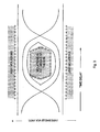
- Fig. 2 is an illustrative example of an industry standard eye mask used to validate the performance of a high speed communications device or subsystem.
- a finite number of eye diagrams representing the output from a target device or subsystem can be overlaid onto a template or mask.
- the eye mask 200 is placed in the center of a representative eye diagram that is comprise of an upper mask boundary or zone 202, a middle polygon 204 and a lower mask boundary or zone 206 shown in gray.
- any sample that occurs above the 1 + Y2 boundary is considered a violation that represents an excessively high signal to noise level.
- Any samples that occur below the 0-Y2 boundary are also violations and represent a very low signal to noise level. While those samples fall into the middle area of the mask, indicating a higher than expected error rate, will tend to close the eye opening too much to permit a satisfactory pass-fail decision.
- Fig. 3 is an illustrative representation showing an eye diagram of an applied data signal transmitted from a target device or subsystem that has been overlaid onto an industry standard eye mask template.
- Fig. 3 shows that unlike the prior art system that uses a limited number of points to form a polygon in the middle of the eye diagram, the present invention performs an iterative loop that accumulates errors or mask violations that might occur for a collection of points along the boundaries of both the upper and lower mask areas 302, 306 as well as around the perimeter of the polygon 304 positioned in the middle of an eye diagram 310. Each these points are set to a specific threshold voltage and variable delay or time setting by a separate, independent processing element or system.
- the independent processing element has been created so effectively as to allow very little time overhead between measurements. This means that many, many points can be measured quickly avoiding the traditional approach where many bits are not part of the bit error rate data because the processing element was busy trying to setup or communicate to the measuring apparatus.
- Fig. 4 illustrates the essential components or elements required to incorporate eye mask test technology and functionality into a binary data bit decision mechanism such as a bit error rate tester in accordance of the present invention.
- the eye mask violation detector 400 is control by a processing element or system (not shown).
- the processing element or system sets and changes threshold voltage levels, variably delayed trigger, selects reference pattern, performs synchronization and count resets and processes all mask segment violations and compiles them into a mask-violation report.
- the essential operative elements of the eye mask violation detector 400 include a decision comparator 302, a variable delayed trigger 412, a sampling flip-flop 410, a multiplexer 414, used to introduce the appropriate reference pattern to a reference comparator 416 and an event counters 418.
- the decision comparator 402 receives and compares the voltage level of the data signal (V s ) from a target device or subsystem against a prescribed threshold voltage (V T ) that can be either above or below the voltage level of the applied data signal. If the voltage level (V s ) is different then that of the threshold voltage (V T ), the output from that decision comparator goes high and sets the bit sampling flip-flop 410. In addition, a series of triggered pulses are also supplied to the bit sampling flip-flop 410 from the variable delay trigger 410.
- Fig 4 shows the output from decision comparator 302 as well as the output of a trigger pulse from variable delayed trigger 412 is applied to bit sampling flip-flop 410.
- the bit sampling flip-flop 410 then, in turn, generates a sequence of bits that indicate that the voltage level of the applied data signal is either above or below the threshold voltage for a specified instance in time.
- the resultant output from the bit sampling flip-flop 410 is then supplied to reference comparator 416 along with a reference bit pattern from multiplexer 414.
- the reference bit pattern that is supplied to comparator 416 is a predetermined bit pattern that can be either all "0"s 404, all "1"s 406 or a user specified NRZ data sequence 408 that is selected by a separate and independent processing element or system (not shown).
- Reference comparator 418 then compares the resultant output from the bit sampling flip-flop 410 to the reference bit pattern produced by multiplexer 414 and if the output from bit sampling flip-flop 410 matches the bit pattern produced by the multiplexer 414, nothing is counted. However, if the two patterns do not match then the resultant output from reference comparator 416 is a mismatch that is collected and recorded as a mask violation by the event counter 418.
- the event counter 418 will increment at the rising edge of each trigger pulse and accumulates the mask violations as "events" for a particular time and voltage level. The events are then forwarded to the processing element or system (not shown) for further processing and evaluation to determine the performance characteristics of the target device or subsystem.
- Fig. 5 is a schematic diagram of a variable delay trigger used in accordance with the present invention.
- the self-extracting trigger mechanism 500 includes a phase comparer 502, a small operation amplifier 504, low pass filter 506, voltage-controlled oscillator 508 and a variable phase control 512.
- the phase comparer compares the phase of the incoming bit stream with that of prescribed trigger pulse.
- the output from the phase comparator 502 as well as a specified voltage from the variable phase adjustment is directed to the operational amplifier 504. The result is then passed to the low pass filter 506 that eliminates any signal inconsistencies.
- the voltage-controlled oscillator 508 provides enough of an additional input, as feedback, to the phase comparer 504 to align leading edge of the pulse from the applied signal with the leading edge of the trigger pulse.
- the phase of the trigger can be adjusted to suit the requirements of a user-specified application by means the variable phase controller 512.
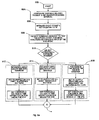
- FIG. 6a and 6b form together a flowchart that illustrates a method of characterizing the performance of an applied signal transmitted from a target device or subsystem using a eye mask test in accordance with the present invention as depicted in FIG. 4.
- the steps in the flowchart are simply illustrative of the functional steps performed by a binary data bit decision mechanism to accumulate the number of mask violation at various instances in time and voltage offsets for a multi-valued data signal transmitted from either a communication device or subsystem that deviates across the boundaries and into one or more of the bounded areas or zones as defined by an eye mask.
- the eye test system or facility is initializing the event counter, configuring the variable delayed trigger to supply the proper trigger pulse.
- the eye mask test facility or system receives a command request to test the applied data signal for mask violations in a specific portion of the eye mask from the program element or system.
- the appropriate segment of the eye mask is then selected.
- the test facility or system control from the program element or system sets the multiplexer to supply the proper reference pattern and set the threshold voltage and time interval values, as well.
- the multiplexer is set to supply a reference bit pattern of all "0"s and the initial threshold voltage-time interval values above the eye diagram are specified.
- the multiplexer For mask violations in the bounded area below the eye diagram, at step 614, the multiplexer is set to supply a reference bit pattern of all "1"s and the initial threshold voltage-time interval values below the eye diagram are specified. Lastly, to determine the mask violations in the polygon bounded area in the middle of the eye diagram, at step 616, the multiplexer supplies a reference bit pattern a NRZ data sequence and the initial threshold voltage-time interval values that are in the middle of the eye diagram are specified.
- Fig. 6b shows, at step 618, the threshold voltage is applied to the decision comparator and if the voltage level of the applied data signal exceeds the voltage threshold (V T ), at step 620, it is compared with the supplied reference bit pattern from the multiplexer. If there are mismatches, at step 624, the event counter is incremented and the mismatches, now considered events, are accumulated for specified period of time. The count of these "events" depicts the number of times the applied data signal deviates into either the upper bounded area or the lower bounded area or into the bounded area in the middle of the eye diagram.
- the process waits for the next trigger to "fire.” Once the reference trigger has "fired” the process of accumulating of the applied data signal that includes steps 620-624 is repeated until time expires. If time interval has expired, at step 626, the number of events accumulated by the event counter, at step 630, is then transferred to the program element or system for additional processing. Once the transfer has been completed, at step 632, the event counter is reset while, at step 636, the next threshold voltage-time interval point is set and steps 618-632 are repeated until all threshold voltage-time interval points have been completely processed.
- the eye mask testing process returns to step 610 to continue the eye mask test, allowing the processing element or system to select a new bounded area for evaluation. This selection process continues until all of the bounded area in the eye mask has been used.
Landscapes
- Engineering & Computer Science (AREA)
- Physics & Mathematics (AREA)
- Computer Networks & Wireless Communication (AREA)
- Signal Processing (AREA)
- General Engineering & Computer Science (AREA)
- General Physics & Mathematics (AREA)
- Nonlinear Science (AREA)
- Quality & Reliability (AREA)
- Dc Digital Transmission (AREA)
- Detection And Prevention Of Errors In Transmission (AREA)
Priority Applications (2)
| Application Number | Priority Date | Filing Date | Title |
|---|---|---|---|
| EP03006064A EP1460793A1 (de) | 2003-03-19 | 2003-03-19 | Verfahren und Vorrichtung zur Fehlerzählung eines ausserhalb des Bereiches einer Augenmaske liegenden Datensignals |
| JP2003077709A JP2004289388A (ja) | 2003-03-19 | 2003-03-20 | アイマスクの範囲外に存在する多値データ信号のエラーを決定する方法及びその装置 |
Applications Claiming Priority (2)
| Application Number | Priority Date | Filing Date | Title |
|---|---|---|---|
| EP03006064A EP1460793A1 (de) | 2003-03-19 | 2003-03-19 | Verfahren und Vorrichtung zur Fehlerzählung eines ausserhalb des Bereiches einer Augenmaske liegenden Datensignals |
| JP2003077709A JP2004289388A (ja) | 2003-03-19 | 2003-03-20 | アイマスクの範囲外に存在する多値データ信号のエラーを決定する方法及びその装置 |
Publications (1)
| Publication Number | Publication Date |
|---|---|
| EP1460793A1 true EP1460793A1 (de) | 2004-09-22 |
Family
ID=33454318
Family Applications (1)
| Application Number | Title | Priority Date | Filing Date |
|---|---|---|---|
| EP03006064A Withdrawn EP1460793A1 (de) | 2003-03-19 | 2003-03-19 | Verfahren und Vorrichtung zur Fehlerzählung eines ausserhalb des Bereiches einer Augenmaske liegenden Datensignals |
Country Status (2)
| Country | Link |
|---|---|
| EP (1) | EP1460793A1 (de) |
| JP (1) | JP2004289388A (de) |
Cited By (6)
| Publication number | Priority date | Publication date | Assignee | Title |
|---|---|---|---|---|
| EP1560034B1 (de) * | 2004-02-02 | 2008-03-05 | Synthesys Research, Inc. | Verfahren und Vorrichtung zur Messung und Anzeige von Augenmustermessungen |
| EP2058668A1 (de) * | 2007-11-12 | 2009-05-13 | Tektronix, Inc. | Trigger auf Verletzung des Augendiagramms und Jitterüberschuss |
| US8327196B2 (en) | 2008-07-16 | 2012-12-04 | International Business Machines Corporation | Identifying an optimized test bit pattern for analyzing electrical communications channel topologies |
| CN109669669A (zh) * | 2018-12-06 | 2019-04-23 | 青岛镕铭半导体有限公司 | 误码生成方法及误码生成器 |
| US10749643B2 (en) | 2016-02-05 | 2020-08-18 | Denso Corporation | Waveform observation system and method for waveform observation |
| WO2023164959A1 (zh) * | 2022-03-02 | 2023-09-07 | 长鑫存储技术有限公司 | 信号眼图分析系统及其方法 |
Families Citing this family (2)
| Publication number | Priority date | Publication date | Assignee | Title |
|---|---|---|---|---|
| JP7266054B2 (ja) | 2021-02-18 | 2023-04-27 | 株式会社日立製作所 | 伝送制御方法、伝送制御システム |
| JP7139476B1 (ja) | 2021-03-24 | 2022-09-20 | アンリツ株式会社 | 波形観測装置及びマスクマージンの計算方法 |
Citations (5)
| Publication number | Priority date | Publication date | Assignee | Title |
|---|---|---|---|---|
| US5228042A (en) * | 1991-02-07 | 1993-07-13 | Northern Telecom Limited | Method and circuit for testing transmission paths |
| US5333147A (en) * | 1991-11-29 | 1994-07-26 | Her Majesty The Queen In Right Of Canada As Represented By The Minister Of Defence | Automatic monitoring of digital communication channel conditions usinhg eye patterns |
| US5761216A (en) * | 1995-02-24 | 1998-06-02 | Advantest Corp. | Bit error measurement system |
| EP1143654A2 (de) * | 2000-04-04 | 2001-10-10 | Synthesys Research, Inc. | Vorrichtung und Verfahren zur statistischen Augenmustermessung von einem seriellen Bitstrom |
| US6430715B1 (en) * | 1999-09-17 | 2002-08-06 | Digital Lightwave, Inc. | Protocol and bit rate independent test system |
-
2003
- 2003-03-19 EP EP03006064A patent/EP1460793A1/de not_active Withdrawn
- 2003-03-20 JP JP2003077709A patent/JP2004289388A/ja active Pending
Patent Citations (5)
| Publication number | Priority date | Publication date | Assignee | Title |
|---|---|---|---|---|
| US5228042A (en) * | 1991-02-07 | 1993-07-13 | Northern Telecom Limited | Method and circuit for testing transmission paths |
| US5333147A (en) * | 1991-11-29 | 1994-07-26 | Her Majesty The Queen In Right Of Canada As Represented By The Minister Of Defence | Automatic monitoring of digital communication channel conditions usinhg eye patterns |
| US5761216A (en) * | 1995-02-24 | 1998-06-02 | Advantest Corp. | Bit error measurement system |
| US6430715B1 (en) * | 1999-09-17 | 2002-08-06 | Digital Lightwave, Inc. | Protocol and bit rate independent test system |
| EP1143654A2 (de) * | 2000-04-04 | 2001-10-10 | Synthesys Research, Inc. | Vorrichtung und Verfahren zur statistischen Augenmustermessung von einem seriellen Bitstrom |
Cited By (8)
| Publication number | Priority date | Publication date | Assignee | Title |
|---|---|---|---|---|
| EP1560034B1 (de) * | 2004-02-02 | 2008-03-05 | Synthesys Research, Inc. | Verfahren und Vorrichtung zur Messung und Anzeige von Augenmustermessungen |
| EP2058668A1 (de) * | 2007-11-12 | 2009-05-13 | Tektronix, Inc. | Trigger auf Verletzung des Augendiagramms und Jitterüberschuss |
| US7983332B2 (en) | 2007-11-12 | 2011-07-19 | Tektronix, Inc. | Eye violation and excess jitter trigger |
| US8327196B2 (en) | 2008-07-16 | 2012-12-04 | International Business Machines Corporation | Identifying an optimized test bit pattern for analyzing electrical communications channel topologies |
| US10749643B2 (en) | 2016-02-05 | 2020-08-18 | Denso Corporation | Waveform observation system and method for waveform observation |
| CN109669669A (zh) * | 2018-12-06 | 2019-04-23 | 青岛镕铭半导体有限公司 | 误码生成方法及误码生成器 |
| CN109669669B (zh) * | 2018-12-06 | 2022-06-24 | 镕铭微电子(济南)有限公司 | 误码生成方法及误码生成器 |
| WO2023164959A1 (zh) * | 2022-03-02 | 2023-09-07 | 长鑫存储技术有限公司 | 信号眼图分析系统及其方法 |
Also Published As
| Publication number | Publication date |
|---|---|
| JP2004289388A (ja) | 2004-10-14 |
Similar Documents
| Publication | Publication Date | Title |
|---|---|---|
| US7310389B2 (en) | Method and apparatus for determining the errors of a multi-valued data signal that are outside the limits of an eye mask | |
| US7606297B2 (en) | Method and system for creating an eye diagram using a binary data bit decision mechanism | |
| EP1267172B1 (de) | Vorrichtung und Verfahren zur auf Spektrumanalyse basierender Messung des Jitters serieller Daten | |
| US6661836B1 (en) | Measuring jitter of high-speed data channels | |
| US7460589B2 (en) | Eye monitoring and reconstruction using CDR and sub-sampling ADC | |
| EP1641172A2 (de) | Verfahren und Gerät für Signalqualitätsanalyse mit verzörgerter Entscheidung | |
| US8024142B1 (en) | Method and system for analyzing signal waveforms | |
| US7519489B2 (en) | Determination of a jitter property of a signal | |
| EP1460793A1 (de) | Verfahren und Vorrichtung zur Fehlerzählung eines ausserhalb des Bereiches einer Augenmaske liegenden Datensignals | |
| JP2006292749A (ja) | ランダムジッタ成分とデターミニスティックジッタ成分の分離 | |
| Dalal et al. | Measuring jitter of high speed data channels using undersampling techniques | |
| US7339985B2 (en) | Zero crossing method of symbol rate and timing estimation | |
| US7788571B2 (en) | Method and apparatus for using dual bit decisions to measure bit errors and event occurrences | |
| US6934647B2 (en) | Efficient sampling of digital waveforms for eye diagram analysis | |
| Li et al. | On the accuracy of jitter separation from bit error rate function | |
| US7080292B2 (en) | Method for testing jitter tolerance of high speed receivers | |
| US11624781B2 (en) | Noise-compensated jitter measurement instrument and methods | |
| US6986091B2 (en) | Method and apparatus for testing a high speed data receiver for jitter tolerance | |
| US20090213918A1 (en) | Separating jitter components in a data stream | |
| EP1460792A1 (de) | Verfahren und System zum Erzeugen eines Augenmusters | |
| US7610520B2 (en) | Digital data signal testing using arbitrary test signal | |
| Kulp | Testing and characterizing jitter in 100BASE-TX and 155.52 Mbit/s ATM devices with a 1 Gsamples/s AWG in an ATE system | |
| Balestrieri et al. | The jitter measurement ways: the jitter graphs | |
| Patrin et al. | Characterizing jitter histograms for clock and datacom applications | |
| WO2005015248A1 (en) | Digital data signal testing using arbitrary test signal |
Legal Events
| Date | Code | Title | Description |
|---|---|---|---|
| PUAI | Public reference made under article 153(3) epc to a published international application that has entered the european phase |
Free format text: ORIGINAL CODE: 0009012 |
|
| AK | Designated contracting states |
Kind code of ref document: A1 Designated state(s): AT BE BG CH CY CZ DE DK EE ES FI FR GB GR HU IE IT LI LU MC NL PT RO SE SI SK TR |
|
| AX | Request for extension of the european patent |
Extension state: AL LT LV MK |
|
| 17P | Request for examination filed |
Effective date: 20050322 |
|
| AKX | Designation fees paid |
Designated state(s): DE FR GB NL |
|
| R17C | First examination report despatched (corrected) |
Effective date: 20070502 |
|
| STAA | Information on the status of an ep patent application or granted ep patent |
Free format text: STATUS: THE APPLICATION IS DEEMED TO BE WITHDRAWN |
|
| 18D | Application deemed to be withdrawn |
Effective date: 20091001 |