EP1457766B1 - Substrate and method of forming substrate for mems device with strain gage - Google Patents
Substrate and method of forming substrate for mems device with strain gage Download PDFInfo
- Publication number
- EP1457766B1 EP1457766B1 EP04251352.3A EP04251352A EP1457766B1 EP 1457766 B1 EP1457766 B1 EP 1457766B1 EP 04251352 A EP04251352 A EP 04251352A EP 1457766 B1 EP1457766 B1 EP 1457766B1
- Authority
- EP
- European Patent Office
- Prior art keywords
- substrate
- strain gage
- angle
- opening
- strain
- Prior art date
- Legal status (The legal status is an assumption and is not a legal conclusion. Google has not performed a legal analysis and makes no representation as to the accuracy of the status listed.)
- Expired - Fee Related
Links
Images
Classifications
-
- G—PHYSICS
- G05—CONTROLLING; REGULATING
- G05F—SYSTEMS FOR REGULATING ELECTRIC OR MAGNETIC VARIABLES
- G05F3/00—Non-retroactive systems for regulating electric variables by using an uncontrolled element, or an uncontrolled combination of elements, such element or such combination having self-regulating properties
- G05F3/02—Regulating voltage or current
- G05F3/08—Regulating voltage or current wherein the variable is dc
-
- B—PERFORMING OPERATIONS; TRANSPORTING
- B41—PRINTING; LINING MACHINES; TYPEWRITERS; STAMPS
- B41J—TYPEWRITERS; SELECTIVE PRINTING MECHANISMS, i.e. MECHANISMS PRINTING OTHERWISE THAN FROM A FORME; CORRECTION OF TYPOGRAPHICAL ERRORS
- B41J2/00—Typewriters or selective printing mechanisms characterised by the printing or marking process for which they are designed
- B41J2/005—Typewriters or selective printing mechanisms characterised by the printing or marking process for which they are designed characterised by bringing liquid or particles selectively into contact with a printing material
- B41J2/01—Ink jet
- B41J2/135—Nozzles
- B41J2/14—Structure thereof only for on-demand ink jet heads
- B41J2/14016—Structure of bubble jet print heads
- B41J2/14153—Structures including a sensor
-
- B—PERFORMING OPERATIONS; TRANSPORTING
- B41—PRINTING; LINING MACHINES; TYPEWRITERS; STAMPS
- B41J—TYPEWRITERS; SELECTIVE PRINTING MECHANISMS, i.e. MECHANISMS PRINTING OTHERWISE THAN FROM A FORME; CORRECTION OF TYPOGRAPHICAL ERRORS
- B41J2/00—Typewriters or selective printing mechanisms characterised by the printing or marking process for which they are designed
- B41J2/005—Typewriters or selective printing mechanisms characterised by the printing or marking process for which they are designed characterised by bringing liquid or particles selectively into contact with a printing material
- B41J2/01—Ink jet
- B41J2/135—Nozzles
- B41J2/14—Structure thereof only for on-demand ink jet heads
- B41J2/14201—Structure of print heads with piezoelectric elements
-
- G—PHYSICS
- G01—MEASURING; TESTING
- G01L—MEASURING FORCE, STRESS, TORQUE, WORK, MECHANICAL POWER, MECHANICAL EFFICIENCY, OR FLUID PRESSURE
- G01L1/00—Measuring force or stress, in general
- G01L1/20—Measuring force or stress, in general by measuring variations in ohmic resistance of solid materials or of electrically-conductive fluids; by making use of electrokinetic cells, i.e. liquid-containing cells wherein an electrical potential is produced or varied upon the application of stress
- G01L1/22—Measuring force or stress, in general by measuring variations in ohmic resistance of solid materials or of electrically-conductive fluids; by making use of electrokinetic cells, i.e. liquid-containing cells wherein an electrical potential is produced or varied upon the application of stress using resistance strain gauges
- G01L1/2206—Special supports with preselected places to mount the resistance strain gauges; Mounting of supports
-
- G—PHYSICS
- G01—MEASURING; TESTING
- G01L—MEASURING FORCE, STRESS, TORQUE, WORK, MECHANICAL POWER, MECHANICAL EFFICIENCY, OR FLUID PRESSURE
- G01L1/00—Measuring force or stress, in general
- G01L1/20—Measuring force or stress, in general by measuring variations in ohmic resistance of solid materials or of electrically-conductive fluids; by making use of electrokinetic cells, i.e. liquid-containing cells wherein an electrical potential is produced or varied upon the application of stress
- G01L1/22—Measuring force or stress, in general by measuring variations in ohmic resistance of solid materials or of electrically-conductive fluids; by making use of electrokinetic cells, i.e. liquid-containing cells wherein an electrical potential is produced or varied upon the application of stress using resistance strain gauges
- G01L1/2287—Measuring force or stress, in general by measuring variations in ohmic resistance of solid materials or of electrically-conductive fluids; by making use of electrokinetic cells, i.e. liquid-containing cells wherein an electrical potential is produced or varied upon the application of stress using resistance strain gauges constructional details of the strain gauges
- G01L1/2293—Measuring force or stress, in general by measuring variations in ohmic resistance of solid materials or of electrically-conductive fluids; by making use of electrokinetic cells, i.e. liquid-containing cells wherein an electrical potential is produced or varied upon the application of stress using resistance strain gauges constructional details of the strain gauges of the semi-conductor type
-
- H—ELECTRICITY
- H02—GENERATION; CONVERSION OR DISTRIBUTION OF ELECTRIC POWER
- H02M—APPARATUS FOR CONVERSION BETWEEN AC AND AC, BETWEEN AC AND DC, OR BETWEEN DC AND DC, AND FOR USE WITH MAINS OR SIMILAR POWER SUPPLY SYSTEMS; CONVERSION OF DC OR AC INPUT POWER INTO SURGE OUTPUT POWER; CONTROL OR REGULATION THEREOF
- H02M1/00—Details of apparatus for conversion
- H02M1/0045—Converters combining the concepts of switch-mode regulation and linear regulation, e.g. linear pre-regulator to switching converter, linear and switching converter in parallel, same converter or same transistor operating either in linear or switching mode
Definitions
- the present invention relates to a substrate for a MEMS device, a method of forming the same and to a fluid ejection device.
- MEMS devices incorporating strain gages.
- Strain gages have been developed for measuring stresses in structures.
- Conventional strain gages include metallic foil type strain gages and semiconductor type strain gages.
- Metallic foil type strain gages typically include a wire having an electrical resistance which varies when subjected to stress.
- Semiconductor type strain gages typically include a piezoresistive material which varies in resistance when subjected to stress. Use of a conventional strain gage requires that the strain gage be fastened or adhered to the structure being measured for stresses.
- Microelectromechanical systems or MEMS devices include micromachined substrates integrated with electronic microcircuits. Such devices may form, for example, microsensors or microactuators which operate based on, for example, electromagnetic, electrostrictive, thermoelectric, piezoelectric, or piezoresistive effects.
- Conventional strain gages are often unsuitable for measuring stresses in a MEMS device.
- conventional strain gages are often larger than the MEMS device itself.
- fastening or adhering a conventional strain gage to the MEMS device may actually increase the strength of the MEMS device, thereby reducing stress in the MEMS device and providing an inaccurate measurement of the actual stress in the MEMS device.
- US 6,398,329 discloses a backpressure sensor that is integrated into a printhead die, or alternatively to a pen body.
- the backpressure sensor is susceptible to ink pressure from ink within a printhead ink slot, ink channel or nozzle chamber, and to ambient pressure.
- the backpressure sensor is susceptible to ink pressure from ink within an ink slot, ink channel or ink cavity away from a printhead die, and to ambient pressure.
- US 6,001,666 discloses the manufacture of a strain gauge sensor using the piezoresistive effect, comprising a structure made of a monocrystalline material acting as support to at least one strain gauge made of a semiconducting material with a freely chosen doping type.
- the strain gauge is an element made along a crystallographic plane determined to improve its piezoresistivity coefficient.
- the structure is a structure etched along a crystallographic plane determined to improve its etching.
- the strain gauge is fixed to the structure by bonding means capable of obtaining said sensor.
- WO 02/101347 discloses an entirely surface micromachined free hanging strain-gauge pressure sensor.
- the sensing element consists of a 80 ⁇ m long H-shaped double ended supported force transducing beam.
- the beam is located beneath and at one end attached to a square polysilicon diaphragm and at the other end to the cavity edge.
- the sensor according to the invention enables a combination of high pressure sensitivity and miniature chip size as well as good environmental isolation.
- the pressure sensitivity for the sensor with a H-shaped force transducing beam, 0.4 ⁇ m thick was found to be 5 ⁇ V/V/mmHg.
- a substrate for a MEMS device as set out at claim 1
- a fluid ejection device as set out at claim 14.
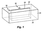
- FIG. 1 illustrates one embodiment of a substrate 20 for a microelectromechanical system or MEMS device.
- the MEMS device may include, for example, a microsensor or a microactuator and may operate based on, for example, electromagnetic, electrostrictive, thermoelectric, piezoelectric, or piezoresistive effects.
- substrate 20 has a first side 22 and a second side 24. Second side 24 is opposite of first side 22 and, in one embodiment, oriented substantially parallel with first side 22. In addition, substrate 20 has an opening 26 formed therethrough. Opening 26 is formed through substrate 20 so as to communicate with first side 22 and second side 24.
- strain gages 30 are integrated in substrate 20. More specifically, strain gages 30 are formed in one or more layers of substrate 20, as described below. As such, strain gages 30 can measure strain in substrate 20, for example, before, after, and/or during processing of substrate 20, fabrication of a MEMS device incorporating substrate 20, and/or operation of a MEMS device including substrate 20.
- strain gages 30 are formed in first side 22 of substrate 20.
- strain gages 30 are typically formed adjacent to opening 26.
- one or more strain gages 30 may be formed at an end of opening 26 or along a side of opening 26.
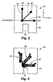
- Figure 2 illustrates one embodiment of a strain gage 30 formed at an end of opening 26 in substrate 20.
- strain gage 30 includes one or more elements oriented relative to each other for measuring strain in one or more axes of substrate 20.
- strain gage 30 includes a first element 32 oriented at a first angle with respect to an axis of substrate 20 for measuring strain in a first axis, a second element 34 oriented at a second angle for measuring strain in a second axis, and a third element 36 oriented at a third angle for measuring strain in a third axis.
- second element 34 is oriented substantially perpendicular to first element 32
- third element 36 substantially bisects the angle between first element 32 and second element 34.
- first element 32, second element 34, and third element 36 form a rosette.
- first element 32 is oriented at a first angle with respect to an axis of substrate 20 of approximately zero degrees
- second element 34 is oriented at a second angle of approximately 90 degrees
- third element 36 is oriented at a third angle of approximately 45 degrees.
- first element 32 is sensitive to strain in an X direction
- second element 34 is sensitive to strain in a Y direction
- third element 36 is sensitive to strain in an XY direction.
- strain in substrate 20 causes a change in resistance of strain gage 30 including, more specifically, a change in resistance of first element 32, second element 34, and/or third element 36.
- first element 32, second element 34, and third element 36 each include first and second terminals 321 and 322, 341 and 342, and 361 and 362, respectively.
- second terminals 322, 342, and 362 are combined as one common terminal. Resistance of strain gage.30 can be measured by electrical coupling to the terminals and incorporating strain gage 30 in an electrical circuit, as described below.
- Figure 3 illustrates another embodiment of a strain gage 30' formed at an end of opening 26 in substrate 20.
- strain gage 30' includes a first element 32', a second element 34', and a third element 36' for measuring strain in X, Y, and XY axes, respectively, of substrate 20.
- first element 32', second element 34', and third element 36' each include multiple legs. As such, an effective length of each element of strain gage 30' is increased. Thus, a resistance of each element of strain gage 30' is increased.
- R pL / tw
- R represents the resistance of the strain gage
- p represents the bulk resistivity of the strain gage material
- L represents the effective length of the strain gage
- t represents the thickness of the strain gage
- w represents the width of the strain gage
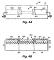
- FIGS 4A and 4B illustrate one embodiment of integrating or forming strain gage 30 in substrate 20.
- strain gage 30 is illustrated as including one element having electrical terminals 301 and 302. It is understood, however, that strain gage 30 may include one or more elements oriented relative to each other for measuring strain in one or more axes of substrate 20, as described above.
- strain gage 30 is formed in first side 22 of substrate 20.
- substrate 20 includes a base material 40.
- strain gage 30 is formed over base material 40 of substrate 20.
- Base material 40 has a first side 42 and a second side 44 opposite first side 42.
- strain gage 30 is formed on first side 42 of base material 40.
- base material 40 is formed of silicon.
- an insulating or dielectric layer 50 is formed over first side 42 of base material 40.
- Dielectric layer 50 may include an oxide which is thermally grown on base material 40 or deposited on base material 40 by, for example, chemical vapor deposition (CVD) or plasma enhanced CVD (PECVD).
- dielectric layer 50 may include, for example, tetraethylorthosilicate (TEOS), silane, silicon dioxide, silicon carbide, silicon nitride, or any other suitable material.
- TEOS tetraethylorthosilicate
- strain gage 30 is formed on dielectric layer 50. Strain gage 30 is formed by deposition and patterned by photolithography and etching to define strain gage 30, including electrical terminals 301 and 302 of strain gage 30. In one embodiment, strain gage 30 is formed of a polycrystalline silicon (poly silicon) material. In one embodiment, the poly silicon material of strain gage 30 is doped with a dopant material, such as boron or phosphorous, and annealed so as to achieve a desired resistance.
- a dopant material such as boron or phosphorous
- Dielectric material 52 is deposited over strain gage 30 and dielectric layer 50.
- Dielectric material 52 may include an oxide such as phosphosilicate glass (PSG), tetraethylorthosilicate (TEOS), or any other suitable material.
- PSG phosphosilicate glass
- TEOS tetraethylorthosilicate
- conductive paths 601 and 602 are formed to respective electrical terminals 301 and 302 of strain gage 30.
- openings 541 and 542 are formed in dielectric material 52 to respective electrical terminals 301 and 302.
- conductive paths 601 and 602 are formed by depositing a conductive material 62 in openings 541 and 542 formed in dielectric material 52.
- conductive material 62 is deposited over dielectric material 52 to form bond pads 641 and 642 for electrical connection to strain gage 30.
- Conductive material 62 may include, for example, aluminum, gold, or any other suitable material.
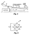
- Figure 5 illustrates one embodiment of calibrating strain gage 30 integrated in substrate 20.
- Strain gage 30 is calibrated by supporting a first end 201 of substrate 20 and subjecting a second end 202 of substrate 20 to a load. As such, second end 202 of substrate 20 is displaced by the load. Thus, strain is created in substrate 20.
- strain in substrate 20 is calculated for varying displacements (Y) of substrate 20.
- strain gage 30 is electrically coupled to a resistance measuring device 70, such as an ohmmeter, to measure the resistance of strain gage 30 under the influence of a known load.
- strain gage 30 is electrically coupled to resistance measuring device 70 by mounting a flexible electrical circuit 72 on substrate 20, and forming an electrical connection between electrical terminals (for example, electrical terminals 301 and 302 of Figures 4A and 4B ) of strain gage 30 and flexible electrical circuit 72 and an electrical connection between flexible electrical circuit 72 and resistance measuring device 70.
- Electrical connection between electrical terminals of strain gage 30 and flexible electrical circuit 72 is formed, for example, by ball bonds. Electrical connection between flexible electrical circuit 72 and resistance measuring device 70 is illustrated, for example, by leads 71.
- strain gage 30 To establish a sensitivity or gage factor (GF) of strain gage 30, the resistance (R) of strain gage 30 is measured as the displacement (Y) of second end 202 of substrate 20 is varied. As such, the change in resistance (dR/R) of strain gage 30 versus strain (e) in substrate 20 is plotted. Thus, the slope of the linear regression of the data represents the gage factor (GF) of strain gage 30.
- strain gage 30 is incorporated in a strain measuring circuit 80.
- strain measuring circuit 80 includes a full-bridge Wheatstone bridge circuit.
- an input voltage (Vin) an output voltage (Vout) is generated in response to stresses developed in substrate 20.
- positive strain represents tensile stresses in substrate 20 and negative strain represents compressive stresses in substrate 20.
- Strain output of strain measuring circuit 80 is naturally temperature compensated since resistance changes due to temperature are equal for all strain gage elements.
- strain gage 30 is incorporated in strain measuring circuit 80 such that strain gage 30 constitutes one or more of the resistive elements provided between nodes a, b, c, and d of strain measuring circuit 80.
- strain gage 30 may be incorporated in strain measuring circuit 80 so as to form a quarter-bridge circuit, a half-bridge circuit, or a full-bridge circuit.
- element 32 of strain gage 30 constitutes the resistive element provided between nodes a and b
- element 34 of strain gage 30 constitutes the resistive element provided between nodes b and c while the resistive elements provided between nodes c and d and nodes d and a are formed by resistors of known values.
- output of strain measuring circuit 80 can be used to measure strain in X and Y directions.
- strain gage 30 With opening 26 formed through substrate 20, stress concentrations are generally higher around opening 26 including, more specifically, at the ends of opening 26. Thus, by forming strain gage 30 in substrate 20 adjacent opening 26, strain gage 30 provides a sensitive device for measuring stresses in substrate 20.
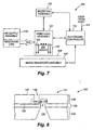
- Figure 7 illustrates one embodiment of an inkjet printing system 100.
- Inkjet printing system 100 constitutes one embodiment of a fluid ejection system which includes a fluid ejection assembly, such as an inkjet printhead assembly 102, and a fluid supply assembly, such as an ink supply assembly 104.
- inkjet printing system 100 also includes a mounting assembly 106, a media transport assembly 108, and an electronic controller 110.
- Inkjet printhead assembly 102 includes one or more printheads or fluid ejection devices which eject drops of ink or fluid through a plurality of orifices or nozzles 103.
- One or more of the printheads may include a substrate with an integrated strain gage according to the present invention.
- the drops are directed toward a medium, such as print medium 109, so as to print onto print medium 109.
- Print medium 109 is any type of suitable sheet material, such as paper, card stock, transparencies, Mylar, and the like.
- nozzles 103 are arranged in one or more columns or arrays such that properly sequenced ejection of ink from nozzles 103 causes, in one embodiment, characters, symbols, and/or other graphics or images to be printed upon print medium 109 as inkjet printhead assembly 102 and print medium 109 are moved relative to each other.
- Ink supply assembly 104 supplies ink to printhead assembly 102 and includes a reservoir 105 for storing ink. As such, in one embodiment, ink flows from reservoir 105 to inkjet printhead assembly 102. In one embodiment, inkjet printhead assembly 102 and ink supply assembly 104 are housed together in an inkjet or fluidjet cartridge or pen. In another embodiment, ink supply assembly 104 is separate from inkjet printhead assembly 102 and supplies ink to inkjet printhead assembly 102 through an interface connection, such as a supply tube.
- Mounting assembly 106 positions inkjet printhead assembly 102 relative to media transport assembly 108 and media transport assembly 108 positions print medium 109 relative to inkjet printhead assembly 102.
- a print zone 107 is defined adjacent to nozzles 103 in an area between inkjet printhead assembly 102 and print medium 109.
- inkjet printhead assembly 102 is a scanning type printhead assembly and mounting assembly 106 includes a carriage for moving inkjet printhead assembly 102 relative to media transport assembly 108.
- inkjet printhead assembly 102 is a non-scanning type printhead assembly and mounting assembly 106 fixes inkjet printhead assembly 102 at a prescribed position relative to media transport assembly 108.
- Electronic controller 110 communicates with inkjet printhead assembly 102, mounting assembly 106, and media transport assembly 108.
- Electronic controller 110 receives data 111 from a host system, such as a computer, and includes memory for temporarily storing data 111.
- data 111 is sent to inkjet printing system 100 along an electronic, infrared, optical or other information transfer path.
- Data 111 represents, for example, a document and/or file to be printed. As such, data 111 forms a print job for inkjet printing system 100 and includes one or more print job commands and/or command parameters.
- electronic controller 110 provides control of inkjet printhead assembly 102 including timing control for ejection of ink drops from nozzles 103.
- electronic controller 110 defines a pattern of ejected ink drops which form characters, symbols, and/or other graphics or images on print medium 109. Timing control and, therefore, the pattern of ejected ink drops, is determined by the print job commands and/or command parameters.
- logic and drive circuitry forming a portion of electronic controller 110 is located on inkjet printhead assembly 102. In another embodiment, logic and drive circuitry is located off inkjet printhead assembly 102.
- Figure 8 illustrates one embodiment of a portion of a fluid ejection device 130 of inkjet printhead assembly 102.
- Fluid ejection device 130 includes an array of drop ejecting elements 131.
- Drop ejecting elements 131 are formed on a substrate 140 which has a fluid (or ink) feed slot 141 formed therein.
- fluid feed slot 141 provides a supply of fluid (or ink) to drop ejecting elements 131.
- Substrate 140 is formed, for example, of silicon, glass, or a stable polymer.
- each drop ejecting element 131 includes a thin-film structure 132 with a firing resistor 134, and an orifice layer 136.
- Thin-film structure 132 has a fluid (or ink) feed hole 133 formed therein which communicates with fluid feed slot 141 of substrate 140.
- Orifice layer 136 has a front face 137 and a nozzle opening 138 formed in front face 137.
- Orifice layer 136 also has a nozzle chamber 139 formed therein which communicates with nozzle opening 138 and fluid feed hole 133 of thin-film structure 132.
- Firing resistor 134 is positioned within nozzle chamber 139 and includes leads 135 which electrically couple firing resistor 134 to a drive signal and ground.
- Thin-film structure 132 is formed, for example, by one or more passivation or insulation layers of silicon dioxide, silicon carbide, silicon nitride, tetraethylorthosilicate (TEOS), or other suitable material.
- thin-film structure 132 also includes a conductive layer which defines firing resistor 134 and leads 135.
- the conductive layer is formed, for example, by poly-silicon, aluminum, gold, tantalum, tantalum-aluminum, or other metal or metal alloy.
- fluid flows from fluid feed slot 141 to nozzle chamber 139 via fluid feed hole 133.
- Nozzle opening 138 is operatively associated with firing resistor 134 such that droplets of fluid are ejected from nozzle chamber 139 through nozzle opening 138 (e.g., normal to the plane of firing resistor 134) and toward a medium upon energization of firing resistor 134.
- Example embodiments of fluid ejection device 130 include a thermal printhead, as previously described, a piezoelectric printhead, a flex-tensional printhead, or any other type of fluidjet ejection device known in the art.
- fluid ejection device 130 is a fully integrated thermal inkjet printhead.
- substrate 20 represents substrate 140 and thin-film structure 132 of fluid ejection device 130
- opening 26 represents fluid feed slot 141 formed in substrate 140 and fluid feed hole 133 formed in thin-film structure 132.
- drop ejecting elements 131 of fluid ejection device 130 are formed on first side 42 of base material 40 and strain gage 30 is formed in thin-film structure 132 of fluid ejection device 130.
- fluid ejection device 130 represents one example of a MEMS device which can have a substrate with a strain gage integrated therein according to the present invention.
- substrate 20 having opening 26 formed therein may be incorporated into other fluid ejection systems including non-printing applications or systems, as well as other devices having fluidic channels through a substrate, such as medical devices. Accordingly, the present invention is not limited to printheads, but is applicable to any slotted substrates.
Description
- The present invention relates to a substrate for a MEMS device, a method of forming the same and to a fluid ejection device. In particular it relates to MEMS devices incorporating strain gages.
- Strain gages have been developed for measuring stresses in structures. Conventional strain gages include metallic foil type strain gages and semiconductor type strain gages. Metallic foil type strain gages typically include a wire having an electrical resistance which varies when subjected to stress. Semiconductor type strain gages typically include a piezoresistive material which varies in resistance when subjected to stress. Use of a conventional strain gage requires that the strain gage be fastened or adhered to the structure being measured for stresses.
- Microelectromechanical systems or MEMS devices include micromachined substrates integrated with electronic microcircuits. Such devices may form, for example, microsensors or microactuators which operate based on, for example, electromagnetic, electrostrictive, thermoelectric, piezoelectric, or piezoresistive effects.
- Conventional strain gages are often unsuitable for measuring stresses in a MEMS device. For example, conventional strain gages are often larger than the MEMS device itself. In addition, fastening or adhering a conventional strain gage to the MEMS device may actually increase the strength of the MEMS device, thereby reducing stress in the MEMS device and providing an inaccurate measurement of the actual stress in the MEMS device.
- Accordingly, there is a need for the present invention.
-
US 6,398,329 discloses a backpressure sensor that is integrated into a printhead die, or alternatively to a pen body. The backpressure sensor is susceptible to ink pressure from ink within a printhead ink slot, ink channel or nozzle chamber, and to ambient pressure. For the alternative embodiment, the backpressure sensor is susceptible to ink pressure from ink within an ink slot, ink channel or ink cavity away from a printhead die, and to ambient pressure. -
US 6,001,666 discloses the manufacture of a strain gauge sensor using the piezoresistive effect, comprising a structure made of a monocrystalline material acting as support to at least one strain gauge made of a semiconducting material with a freely chosen doping type. The strain gauge is an element made along a crystallographic plane determined to improve its piezoresistivity coefficient. The structure is a structure etched along a crystallographic plane determined to improve its etching. The strain gauge is fixed to the structure by bonding means capable of obtaining said sensor. -
WO 02/101347 - According to the present invention, there is provided a substrate for a MEMS device as set out at claim 1, a method of forming a substrate as set out at claim 10, and a fluid ejection device as set out at claim 14.
- A number of preferred embodiments of the invention will now be described with reference to the drawings, in which:-
-
Figure 1 is a schematic perspective view illustrating one embodiment of a substrate for a MEMS device according to the present invention. -
Figure 2 is a schematic plan view of a portion of the substrate ofFigure 1 illustrating one embodiment of a strain gage integrated in the substrate. -
Figure 3 is a schematic plan view of a portion of the substrate ofFigure 1 illustrating another embodiment of a strain gage integrated in the substrate. -
Figures 4A and 4B are schematic illustrations of one embodiment of a strain gage integrated in a substrate according to the present invention. -
Figure 5 is a schematic illustration of one embodiment of calibrating a strain gage integrated in a substrate according to the present invention. -
Figure 6 is a schematic diagram illustrating one embodiment of a strain measuring circuit incorporating a strain gage according to the present invention. -
Figure 7 is a block diagram illustrating one embodiment of a fluid ejection system including a fluid ejection assembly formed with a substrate having an integrated strain gage according to the present invention. -
Figure 8 is a schematic cross-sectional view illustrating one embodiment of a portion of a fluid ejection device. - In the following detailed description of the preferred embodiments, reference is made to the accompanying drawings which form a part hereof, and in which is shown by way of illustration specific embodiments in which the invention may be practiced. In this regard, directional terminology, such as "top,""bottom," "front," "back," "leading,""trailing," etc., is used with reference to the orientation of the Figure(s) being described. Because components of the present invention can be positioned in a number of different orientations, the directional terminology is used for purposes of illustration and is in no way limiting. It is to be understood that other embodiments may be utilized and structural or logical changes may be made without departing from the scope of the present invention. The following detailed description, therefore, is not to be taken in a limiting sense, and the scope of the present invention is defined by the appended claims.
-
Figure 1 illustrates one embodiment of asubstrate 20 for a microelectromechanical system or MEMS device. The MEMS device may include, for example, a microsensor or a microactuator and may operate based on, for example, electromagnetic, electrostrictive, thermoelectric, piezoelectric, or piezoresistive effects. - In one embodiment,
substrate 20 has afirst side 22 and asecond side 24.Second side 24 is opposite offirst side 22 and, in one embodiment, oriented substantially parallel withfirst side 22. In addition,substrate 20 has anopening 26 formed therethrough.Opening 26 is formed throughsubstrate 20 so as to communicate withfirst side 22 andsecond side 24. - As illustrated schematically in the embodiment of
Figure 1 , one ormore strain gages 30 are integrated insubstrate 20. More specifically,strain gages 30 are formed in one or more layers ofsubstrate 20, as described below. As such,strain gages 30 can measure strain insubstrate 20, for example, before, after, and/or during processing ofsubstrate 20, fabrication of a MEMSdevice incorporating substrate 20, and/or operation of a MEMSdevice including substrate 20. - In one embodiment,
strain gages 30 are formed infirst side 22 ofsubstrate 20. In addition,strain gages 30 are typically formed adjacent to opening 26. For example, one ormore strain gages 30 may be formed at an end of opening 26 or along a side of opening 26. -
Figure 2 illustrates one embodiment of astrain gage 30 formed at an end of opening 26 insubstrate 20. In one embodiment,strain gage 30 includes one or more elements oriented relative to each other for measuring strain in one or more axes ofsubstrate 20. For example,strain gage 30 includes afirst element 32 oriented at a first angle with respect to an axis ofsubstrate 20 for measuring strain in a first axis, asecond element 34 oriented at a second angle for measuring strain in a second axis, and athird element 36 oriented at a third angle for measuring strain in a third axis. In one embodiment,second element 34 is oriented substantially perpendicular tofirst element 32, andthird element 36 substantially bisects the angle betweenfirst element 32 andsecond element 34. As such,first element 32,second element 34, andthird element 36 form a rosette. - In one illustrative embodiment,
first element 32 is oriented at a first angle with respect to an axis ofsubstrate 20 of approximately zero degrees,second element 34 is oriented at a second angle of approximately 90 degrees, andthird element 36 is oriented at a third angle of approximately 45 degrees. As such, with respect toFigure 2 ,first element 32 is sensitive to strain in an X direction,second element 34 is sensitive to strain in a Y direction, andthird element 36 is sensitive to strain in an XY direction. - As described below, strain in
substrate 20 causes a change in resistance ofstrain gage 30 including, more specifically, a change in resistance offirst element 32,second element 34, and/orthird element 36. To measure the resistance ofstrain gage 30,first element 32,second element 34, andthird element 36 each include first andsecond terminals strain gage 30 in an electrical circuit, as described below. -
Figure 3 illustrates another embodiment of a strain gage 30' formed at an end of opening 26 insubstrate 20. Similar tostrain gage 30, strain gage 30' includes a first element 32', a second element 34', and a third element 36' for measuring strain in X, Y, and XY axes, respectively, ofsubstrate 20. In one illustrative embodiment, first element 32', second element 34', and third element 36', however, each include multiple legs. As such, an effective length of each element of strain gage 30' is increased. Thus, a resistance of each element of strain gage 30' is increased. The relationship of resistance to length for strain gage 30' is expressed as:
- When strain gage 30' is divided into multiple legs, the effective length (L) of strain gage 30' is expressed as:

-
Figures 4A and 4B illustrate one embodiment of integrating or formingstrain gage 30 insubstrate 20. In this embodiment,strain gage 30 is illustrated as including one element havingelectrical terminals strain gage 30 may include one or more elements oriented relative to each other for measuring strain in one or more axes ofsubstrate 20, as described above. In one embodiment,strain gage 30 is formed infirst side 22 ofsubstrate 20. - As illustrated in
Figure 4B ,substrate 20 includes abase material 40. As such,strain gage 30 is formed overbase material 40 ofsubstrate 20.Base material 40 has afirst side 42 and asecond side 44 oppositefirst side 42. Thus,strain gage 30 is formed onfirst side 42 ofbase material 40. - In one embodiment,
base material 40 is formed of silicon. As such, an insulating ordielectric layer 50 is formed overfirst side 42 ofbase material 40.Dielectric layer 50 may include an oxide which is thermally grown onbase material 40 or deposited onbase material 40 by, for example, chemical vapor deposition (CVD) or plasma enhanced CVD (PECVD). As such,dielectric layer 50 may include, for example, tetraethylorthosilicate (TEOS), silane, silicon dioxide, silicon carbide, silicon nitride, or any other suitable material. - In one embodiment,
strain gage 30 is formed ondielectric layer 50.Strain gage 30 is formed by deposition and patterned by photolithography and etching to definestrain gage 30, includingelectrical terminals strain gage 30. In one embodiment,strain gage 30 is formed of a polycrystalline silicon (poly silicon) material. In one embodiment, the poly silicon material ofstrain gage 30 is doped with a dopant material, such as boron or phosphorous, and annealed so as to achieve a desired resistance. - As illustrated in the embodiment of
Figure 4B , an insulating ordielectric material 52 is deposited overstrain gage 30 anddielectric layer 50.Dielectric material 52 may include an oxide such as phosphosilicate glass (PSG), tetraethylorthosilicate (TEOS), or any other suitable material. - In one embodiment,
conductive paths electrical terminals strain gage 30. To formconductive paths openings dielectric material 52 to respectiveelectrical terminals conductive paths conductive material 62 inopenings dielectric material 52. In addition,conductive material 62 is deposited overdielectric material 52 to formbond pads gage 30.Conductive material 62 may include, for example, aluminum, gold, or any other suitable material. -
Figure 5 illustrates one embodiment of calibratingstrain gage 30 integrated insubstrate 20.Strain gage 30 is calibrated by supporting afirst end 201 ofsubstrate 20 and subjecting asecond end 202 ofsubstrate 20 to a load. As such,second end 202 ofsubstrate 20 is displaced by the load. Thus, strain is created insubstrate 20. Strain insubstrate 20 is expressed as:
substrate 20 is calculated for varying displacements (Y) ofsubstrate 20. - To calibrate
strain gage 30,strain gage 30 is electrically coupled to aresistance measuring device 70, such as an ohmmeter, to measure the resistance ofstrain gage 30 under the influence of a known load. In one embodiment,strain gage 30 is electrically coupled toresistance measuring device 70 by mounting a flexibleelectrical circuit 72 onsubstrate 20, and forming an electrical connection between electrical terminals (for example,electrical terminals Figures 4A and 4B ) ofstrain gage 30 and flexibleelectrical circuit 72 and an electrical connection between flexibleelectrical circuit 72 andresistance measuring device 70. Electrical connection between electrical terminals ofstrain gage 30 and flexibleelectrical circuit 72 is formed, for example, by ball bonds. Electrical connection between flexibleelectrical circuit 72 andresistance measuring device 70 is illustrated, for example, by leads 71. - To establish a sensitivity or gage factor (GF) of
strain gage 30, the resistance (R) ofstrain gage 30 is measured as the displacement (Y) ofsecond end 202 ofsubstrate 20 is varied. As such, the change in resistance (dR/R) ofstrain gage 30 versus strain (e) insubstrate 20 is plotted. Thus, the slope of the linear regression of the data represents the gage factor (GF) ofstrain gage 30. - In one embodiment, as illustrated in
Figure 6 , to measure strain insubstrate 20,strain gage 30 is incorporated in astrain measuring circuit 80. In one embodiment, strain measuringcircuit 80 includes a full-bridge Wheatstone bridge circuit. Thus, with application of an input voltage (Vin), an output voltage (Vout) is generated in response to stresses developed insubstrate 20. As such, strain (e) insubstrate 20 is expressed as:

substrate 20 and negative strain represents compressive stresses insubstrate 20. Strain output ofstrain measuring circuit 80 is naturally temperature compensated since resistance changes due to temperature are equal for all strain gage elements. - In one embodiment,
strain gage 30 is incorporated instrain measuring circuit 80 such thatstrain gage 30 constitutes one or more of the resistive elements provided between nodes a, b, c, and d ofstrain measuring circuit 80. One ormore strain gages 30 may be incorporated instrain measuring circuit 80 so as to form a quarter-bridge circuit, a half-bridge circuit, or a full-bridge circuit. For example, to form a half-bridge circuit withstrain gage 30 including multiple elements as illustrated, for example, inFigure 2 ,element 32 ofstrain gage 30 constitutes the resistive element provided between nodes a and b, andelement 34 ofstrain gage 30 constitutes the resistive element provided between nodes b and c while the resistive elements provided between nodes c and d and nodes d and a are formed by resistors of known values. As such, output ofstrain measuring circuit 80 can be used to measure strain in X and Y directions. - With opening 26 formed through
substrate 20, stress concentrations are generally higher around opening 26 including, more specifically, at the ends ofopening 26. Thus, by formingstrain gage 30 insubstrate 20adjacent opening 26,strain gage 30 provides a sensitive device for measuring stresses insubstrate 20. -
Figure 7 illustrates one embodiment of aninkjet printing system 100.Inkjet printing system 100 constitutes one embodiment of a fluid ejection system which includes a fluid ejection assembly, such as aninkjet printhead assembly 102, and a fluid supply assembly, such as anink supply assembly 104. In the illustrated embodiment,inkjet printing system 100 also includes a mountingassembly 106, amedia transport assembly 108, and anelectronic controller 110. -
Inkjet printhead assembly 102, as one embodiment of a fluid ejection assembly, includes one or more printheads or fluid ejection devices which eject drops of ink or fluid through a plurality of orifices ornozzles 103. One or more of the printheads may include a substrate with an integrated strain gage according to the present invention. In one embodiment, the drops are directed toward a medium, such asprint medium 109, so as to print ontoprint medium 109.Print medium 109 is any type of suitable sheet material, such as paper, card stock, transparencies, Mylar, and the like. Typically,nozzles 103 are arranged in one or more columns or arrays such that properly sequenced ejection of ink fromnozzles 103 causes, in one embodiment, characters, symbols, and/or other graphics or images to be printed uponprint medium 109 asinkjet printhead assembly 102 andprint medium 109 are moved relative to each other. -
Ink supply assembly 104, as one embodiment of a fluid supply assembly, supplies ink toprinthead assembly 102 and includes areservoir 105 for storing ink. As such, in one embodiment, ink flows fromreservoir 105 toinkjet printhead assembly 102. In one embodiment,inkjet printhead assembly 102 andink supply assembly 104 are housed together in an inkjet or fluidjet cartridge or pen. In another embodiment,ink supply assembly 104 is separate frominkjet printhead assembly 102 and supplies ink toinkjet printhead assembly 102 through an interface connection, such as a supply tube. - Mounting assembly 106 positions
inkjet printhead assembly 102 relative tomedia transport assembly 108 andmedia transport assembly 108 positions print medium 109 relative toinkjet printhead assembly 102. Thus, aprint zone 107 is defined adjacent tonozzles 103 in an area betweeninkjet printhead assembly 102 andprint medium 109. In one embodiment,inkjet printhead assembly 102 is a scanning type printhead assembly and mountingassembly 106 includes a carriage for movinginkjet printhead assembly 102 relative tomedia transport assembly 108. In another embodiment,inkjet printhead assembly 102 is a non-scanning type printhead assembly and mountingassembly 106 fixesinkjet printhead assembly 102 at a prescribed position relative tomedia transport assembly 108. -
Electronic controller 110 communicates withinkjet printhead assembly 102, mountingassembly 106, andmedia transport assembly 108.Electronic controller 110 receivesdata 111 from a host system, such as a computer, and includes memory for temporarily storingdata 111. Typically,data 111 is sent toinkjet printing system 100 along an electronic, infrared, optical or other information transfer path.Data 111 represents, for example, a document and/or file to be printed. As such,data 111 forms a print job forinkjet printing system 100 and includes one or more print job commands and/or command parameters. - In one embodiment,
electronic controller 110 provides control ofinkjet printhead assembly 102 including timing control for ejection of ink drops fromnozzles 103. As such,electronic controller 110 defines a pattern of ejected ink drops which form characters, symbols, and/or other graphics or images onprint medium 109. Timing control and, therefore, the pattern of ejected ink drops, is determined by the print job commands and/or command parameters. In one embodiment, logic and drive circuitry forming a portion ofelectronic controller 110 is located oninkjet printhead assembly 102. In another embodiment, logic and drive circuitry is located offinkjet printhead assembly 102. -
Figure 8 illustrates one embodiment of a portion of afluid ejection device 130 ofinkjet printhead assembly 102.Fluid ejection device 130 includes an array ofdrop ejecting elements 131. Drop ejectingelements 131 are formed on asubstrate 140 which has a fluid (or ink)feed slot 141 formed therein. As such,fluid feed slot 141 provides a supply of fluid (or ink) to drop ejectingelements 131.Substrate 140 is formed, for example, of silicon, glass, or a stable polymer. - In one embodiment, each drop ejecting
element 131 includes a thin-film structure 132 with a firingresistor 134, and anorifice layer 136. Thin-film structure 132 has a fluid (or ink)feed hole 133 formed therein which communicates withfluid feed slot 141 ofsubstrate 140.Orifice layer 136 has afront face 137 and anozzle opening 138 formed infront face 137.Orifice layer 136 also has anozzle chamber 139 formed therein which communicates withnozzle opening 138 andfluid feed hole 133 of thin-film structure 132.Firing resistor 134 is positioned withinnozzle chamber 139 and includesleads 135 which electricallycouple firing resistor 134 to a drive signal and ground. - Thin-
film structure 132 is formed, for example, by one or more passivation or insulation layers of silicon dioxide, silicon carbide, silicon nitride, tetraethylorthosilicate (TEOS), or other suitable material. In one embodiment, thin-film structure 132 also includes a conductive layer which defines firingresistor 134 and leads 135. The conductive layer is formed, for example, by poly-silicon, aluminum, gold, tantalum, tantalum-aluminum, or other metal or metal alloy. - In one embodiment, during operation, fluid flows from
fluid feed slot 141 tonozzle chamber 139 viafluid feed hole 133.Nozzle opening 138 is operatively associated with firingresistor 134 such that droplets of fluid are ejected fromnozzle chamber 139 through nozzle opening 138 (e.g., normal to the plane of firing resistor 134) and toward a medium upon energization of firingresistor 134. - Example embodiments of
fluid ejection device 130 include a thermal printhead, as previously described, a piezoelectric printhead, a flex-tensional printhead, or any other type of fluidjet ejection device known in the art. In one embodiment,fluid ejection device 130 is a fully integrated thermal inkjet printhead. - In one embodiment,
substrate 20 representssubstrate 140 and thin-film structure 132 offluid ejection device 130, andopening 26 representsfluid feed slot 141 formed insubstrate 140 andfluid feed hole 133 formed in thin-film structure 132. As such, drop ejectingelements 131 offluid ejection device 130 are formed onfirst side 42 ofbase material 40 andstrain gage 30 is formed in thin-film structure 132 offluid ejection device 130. Thus,fluid ejection device 130 represents one example of a MEMS device which can have a substrate with
a strain gage integrated therein according to the present invention. - While the above description refers to the inclusion of
substrate 20 having
opening 26 formed therein in an inkjet printhead assembly, it is understood thatsubstrate 20 havingopening 26 formed therein may be incorporated into other fluid ejection systems including non-printing applications or systems, as well as other devices having fluidic channels through a substrate, such as medical devices. Accordingly, the present invention is not limited to printheads, but is applicable to any slotted substrates.
Claims (20)
- A substrate (20) for a MEMS device, the substrate comprising:a base material (40) having a first side (42);a strain gage (30) formed on the first side of the base material, the strain gage including a poly silicon material;a dielectric material (52) disposed over the strain gage; anda conductive material (62) in communication with the strain gage through the dielectric material,wherein the substrate has at least one opening (26) formed therethrough, and wherein the strain gage is located adjacent the at least one opening and includes a first element (32) oriented at a first angle with respect to an axis of the substrate, a second element (34) oriented at a second angle, and a third element (36) oriented at a third angle, wherein the second angle is substantially perpendicular to the first angle, and the third angle substantially bisects the first angle and the second angle.
- The substrate of claim 1, further comprising:a dielectric layer (50) formed on the first side of the base material,wherein the strain gage is located on the first side of the base material over the dielectric layer.
- The substrate of claim 2, wherein the base material includes silicon; and wherein the dielectric layer includes one of tetraethylorthosilicate, silane, silicon dioxide, silicon carbide, and silicon nitride.
- The substrate of any preceding claim, wherein the poly silicon material of the strain gage is doped with a dopant material, and wherein the poly silicon material and the dopant material are annealed.
- The substrate of claim 4, wherein the dopant material includes one of boron and phosphorus.
- The substrate of any preceding claim, wherein the dielectric material includes one of phosphosilicate glass and tetraethylorthosilicate.
- The substrate of any preceding claim, wherein the dielectric material has at least one opening (541,542) formed therein to the strain gage, and wherein the conductive material is deposited within the at least one opening in the dielectric material.
- The substrate of claim 1, wherein the MEMS device comprises a fluid ejection device (130), and wherein the at least one opening through the substrate comprises a fluid passage (141;133) through the substrate.
- The substrate of any one of claims 1 to 8, wherein the strain gauge (30) is located at an end of the at least one opening (26).
- A method of forming a substrate (20) for a MEMS device, the method comprising:providing a base material (40) having a first side (42);forming a strain gage (30) on the first side of the base material, the strain gage including a poly silicon material;disposing a dielectric material (52) over the strain gage; andcontacting a conductive material (62) with the strain gage through the dielectric material,wherein the substrate is adapted to have at least one opening (26) formed therethrough, wherein the strain gage is adapted to be formed adjacent the at least one opening, and wherein forming the strain gage includes orienting a first element (32) of the strain gage at a first angle with respect to an axis of the substrate, orienting a second element (34) of the strain gage at a second angle, and orienting a third element (36) of the strain gage at a third angle, wherein the second angle is substantially perpendicular to the first angle and the third angle substantially bisects the first angle and the second angle (26).
- The method of claim 10, further comprising:forming a dielectric layer (50) on the first side of the base material,wherein forming the strain gage includes forming the strain gage on the first side of the base material over the dielectric layer.
- The method of claim 10 or 11, wherein contacting the conductive material with the strain gage includes forming at least one opening (541,542) in the dielectric material to the strain gage and depositing the conductive material within the at least one opening.
- The method of any of claims 10 to 12, wherein the MEMS device comprises a fluid ejection device (130), and wherein the at least one opening through the substrate comprises a fluid passage (141;133) through the substrate.
- A fluid ejection device (130), comprising:a substrate (20/140;132) having at least one opening (26/141;133) formed therethrough;a plurality of drop ejecting elements (131) formed on the substrate; anda strain gage (30) formed in the substrate adjacent the at least one opening,wherein the strain gage includes a first element (32) oriented at a first angle with respect to an axis of the substrate, a second element (34) oriented at a second angle, and a third element (36) oriented at a third angle, wherein the second angle is substantially perpendicular to the first angle, and the third angle substantially bisects the first angle and the second angle.
- The device of claim 14, wherein the strain gage includes a poly silicon material.
- The device of claim 14 or 15, wherein the substrate includes a dielectric material (52) disposed over the strain gage and a conductive material (62) in communication with the strain gage through the dielectric material.
- The device of claim 16, wherein the substrate further includes a base material (40) and a dielectric layer (50) formed on a first side (42) of the base material, and wherein the strain gage is formed on the first side of the base material over the dielectric layer.
- The device of any of claims 14 to 17, wherein the at least one opening comprises a fluid passage through the substrate.
- The device of any of claims 14 to 18, wherein the fluid ejection device includes an inkjet printhead.
- An inkjet printing system (100) comprising:an inkjet printhead assembly (104) comprising one or more fluid ejection devices (130) according to any one of claims 14 to 19;an ink supply assembly (104);a mounting assembly (106);a media transport assembly (108); andan electronic controller (110).
Applications Claiming Priority (2)
| Application Number | Priority Date | Filing Date | Title |
|---|---|---|---|
| US384887 | 2003-03-10 | ||
| US10/384,887 US6739199B1 (en) | 2003-03-10 | 2003-03-10 | Substrate and method of forming substrate for MEMS device with strain gage |
Publications (2)
| Publication Number | Publication Date |
|---|---|
| EP1457766A1 EP1457766A1 (en) | 2004-09-15 |
| EP1457766B1 true EP1457766B1 (en) | 2013-05-08 |
Family
ID=32312413
Family Applications (1)
| Application Number | Title | Priority Date | Filing Date |
|---|---|---|---|
| EP04251352.3A Expired - Fee Related EP1457766B1 (en) | 2003-03-10 | 2004-03-09 | Substrate and method of forming substrate for mems device with strain gage |
Country Status (5)
| Country | Link |
|---|---|
| US (1) | US6739199B1 (en) |
| EP (1) | EP1457766B1 (en) |
| JP (2) | JP4146812B2 (en) |
| KR (1) | KR101083903B1 (en) |
| TW (1) | TWI306831B (en) |
Cited By (4)
| Publication number | Priority date | Publication date | Assignee | Title |
|---|---|---|---|---|
| WO2018199910A1 (en) * | 2017-04-24 | 2018-11-01 | Hewlett-Packard Development Company, L.P. | Fluid back pressure sensing with a strain sensor |
| WO2019017907A1 (en) * | 2017-07-18 | 2019-01-24 | Hewlett-Packard Development Company, L.P. | Dies including strain gauge sensors and temperature sensors |
| CN110446612A (en) * | 2017-04-24 | 2019-11-12 | 惠普发展公司,有限责任合伙企业 | Fluid injection tube core including strain-gage pickup |
| EP4155488A1 (en) * | 2021-09-23 | 2023-03-29 | U-Shin Italia S.p.A. | Detection device and detection system for activating at least on function of an apparatus, and apparatus comprising the detection system |
Families Citing this family (20)
| Publication number | Priority date | Publication date | Assignee | Title |
|---|---|---|---|---|
| JP2004358799A (en) * | 2003-06-04 | 2004-12-24 | Canon Inc | Carriage driving control method |
| US6988412B1 (en) * | 2004-11-30 | 2006-01-24 | Endevco Corporation | Piezoresistive strain concentrator |
| WO2008048212A2 (en) * | 2005-07-07 | 2008-04-24 | The Regents Of The University Of California | Infrared sensor systems and devices |
| US8059385B2 (en) * | 2006-12-05 | 2011-11-15 | Wispry, Inc. | Substrates with slotted metals and related methods |
| JP5026144B2 (en) * | 2007-05-18 | 2012-09-12 | 日本電信電話株式会社 | Memory element |
| KR100917649B1 (en) * | 2007-11-12 | 2009-09-17 | 주식회사 이오테크닉스 | Method and apparatus for flattening flexible substrate |
| WO2010089234A1 (en) * | 2009-02-03 | 2010-08-12 | Oce-Technologies B.V. | A print head and a method for measuring on the print head |
| US7938016B2 (en) * | 2009-03-20 | 2011-05-10 | Freescale Semiconductor, Inc. | Multiple layer strain gauge |
| JP5632964B2 (en) * | 2010-05-27 | 2014-11-26 | ヒューレット−パッカード デベロップメント カンパニー エル.ピー.Hewlett‐Packard Development Company, L.P. | Printhead and related methods and systems |
| GB201117343D0 (en) * | 2011-10-07 | 2011-11-23 | Airbus Uk Ltd | Method and apparatus for measuring residual stresses in a component |
| DE102012208492A1 (en) * | 2012-05-22 | 2013-11-28 | Continental Teves Ag & Co. Ohg | Dehnmessstreifenanordnung |
| US8857271B2 (en) * | 2012-07-24 | 2014-10-14 | The Boeing Company | Wraparound strain gage assembly for brake rod |
| JP6987497B2 (en) * | 2016-01-08 | 2022-01-05 | キヤノン株式会社 | Liquid discharge module and liquid discharge head |
| US10955299B2 (en) * | 2017-04-24 | 2021-03-23 | Hewlett-Packard Development Company, L.P. | Fluid ejection dies including strain gauge sensors |
| WO2018199886A1 (en) * | 2017-04-24 | 2018-11-01 | Hewlett-Packard Development Company, L.P. | Fluid ejection dies including strain gauge sensors |
| CN107329615B (en) * | 2017-06-30 | 2020-06-16 | 上海天马微电子有限公司 | Display panel and display device |
| CN108731858B (en) * | 2018-06-01 | 2019-07-30 | 中国石油大学(华东) | A kind of MEMS pressure sensor and preparation method thereof |
| CN113795386B (en) * | 2019-05-15 | 2023-09-01 | 惠普发展公司,有限责任合伙企业 | Integrated circuit including strain gauge sensor |
| CZ308886B6 (en) * | 2019-10-11 | 2021-08-04 | 4Dot Mechatronic Systems S.R.O. | Deformation sensor and deformation measuring assembly comprising this sensor |
| US11630018B2 (en) * | 2021-03-18 | 2023-04-18 | Becs Technology, Inc. | Calibrated load cell |
Family Cites Families (26)
| Publication number | Priority date | Publication date | Assignee | Title |
|---|---|---|---|---|
| US4373399A (en) | 1981-02-05 | 1983-02-15 | Beloglazov Alexei V | Semiconductor strain gauge transducer |
| US4462018A (en) | 1982-11-05 | 1984-07-24 | Gulton Industries, Inc. | Semiconductor strain gauge with integral compensation resistors |
| JPS59217375A (en) | 1983-05-26 | 1984-12-07 | Toyota Central Res & Dev Lab Inc | Semiconductor mechanic-electric conversion device |
| US4658233A (en) | 1984-03-16 | 1987-04-14 | Fuji Electric Corporate Research & Development Ltd. | Strain gauge |
| US4737473A (en) | 1985-03-26 | 1988-04-12 | Endevco Corporation | Piezoresistive transducer |
| US4793194A (en) | 1985-03-26 | 1988-12-27 | Endevco Corporation | Piezoresistive transducer |
| JPS6276783A (en) * | 1985-09-30 | 1987-04-08 | Toyota Central Res & Dev Lab Inc | Manufacture of semiconductor pressure sensor |
| US4771638A (en) * | 1985-09-30 | 1988-09-20 | Kabushiki Kaisha Toyota Chuo Kenkyusho | Semiconductor pressure sensor |
| JPS6381867A (en) | 1986-09-25 | 1988-04-12 | Yokogawa Electric Corp | Semiconductor diffusion strain gauge |
| JPH03111729A (en) * | 1989-09-26 | 1991-05-13 | Matsushita Electric Works Ltd | Pressure measuring apparatus |
| DE59108247D1 (en) | 1991-11-30 | 1996-11-07 | Endress Hauser Gmbh Co | Process for stabilizing the surface properties of objects to be heat-treated in vacuum |
| US5408253A (en) | 1992-08-03 | 1995-04-18 | Eastman Kodak Company | Integrated galvanometer scanning device |
| US5275055A (en) | 1992-08-31 | 1994-01-04 | Honeywell Inc. | Resonant gauge with microbeam driven in constant electric field |
| US5511427A (en) | 1993-07-21 | 1996-04-30 | Honeywell Inc. | Cantilevered microbeam temperature sensor |
| US5417115A (en) | 1993-07-23 | 1995-05-23 | Honeywell Inc. | Dielectrically isolated resonant microsensors |
| US5742222A (en) | 1995-05-26 | 1998-04-21 | Avi Systems, Inc. | Direct adhering polysilicon based strain gage |
| JPH09232595A (en) | 1996-02-26 | 1997-09-05 | Denso Corp | Pressure detection device |
| FR2746919B1 (en) | 1996-03-28 | 1998-04-24 | Commissariat Energie Atomique | CONSTRAINED GAUGE SENSOR USING THE PIEZORESISTIVE EFFECT AND ITS MANUFACTURING METHOD |
| JPH09318474A (en) | 1996-05-29 | 1997-12-12 | Tokai Rika Co Ltd | Manufacture of sensor |
| US5929875A (en) * | 1996-07-24 | 1999-07-27 | Hewlett-Packard Company | Acoustic and ultrasonic monitoring of inkjet droplets |
| JPH11129472A (en) * | 1997-10-31 | 1999-05-18 | Seiko Epson Corp | Ink-jet head, ink end detector, ink-jet recording apparatus, and control method therefor |
| JP2001138519A (en) * | 1999-11-10 | 2001-05-22 | Casio Comput Co Ltd | Ink jet printing head |
| DE10014984A1 (en) * | 2000-03-25 | 2001-10-18 | Bosch Gmbh Robert | Manufacturing method for a thin-film component, in particular a thin-film high-pressure sensor |
| JP2002131161A (en) * | 2000-10-27 | 2002-05-09 | Denso Corp | Semiconductor pressure sensor |
| US6398329B1 (en) * | 2000-11-13 | 2002-06-04 | Hewlett-Packard Company | Thermal inkjet pen having a backpressure sensor |
| US7017420B2 (en) | 2001-06-08 | 2006-03-28 | Silex Microsystems Ab | Miniaturized pressure sensor |
-
2003
- 2003-03-10 US US10/384,887 patent/US6739199B1/en not_active Expired - Lifetime
- 2003-09-25 TW TW092126532A patent/TWI306831B/en not_active IP Right Cessation
-
2004
- 2004-03-09 KR KR1020040015821A patent/KR101083903B1/en active IP Right Grant
- 2004-03-09 EP EP04251352.3A patent/EP1457766B1/en not_active Expired - Fee Related
- 2004-03-09 JP JP2004065493A patent/JP4146812B2/en not_active Expired - Fee Related
-
2008
- 2008-05-21 JP JP2008132869A patent/JP2008275630A/en active Pending
Cited By (6)
| Publication number | Priority date | Publication date | Assignee | Title |
|---|---|---|---|---|
| WO2018199910A1 (en) * | 2017-04-24 | 2018-11-01 | Hewlett-Packard Development Company, L.P. | Fluid back pressure sensing with a strain sensor |
| CN110446612A (en) * | 2017-04-24 | 2019-11-12 | 惠普发展公司,有限责任合伙企业 | Fluid injection tube core including strain-gage pickup |
| US10926537B2 (en) | 2017-04-24 | 2021-02-23 | Hewlett-Packard Development Company, L.P. | Fluid back pressure sensing with a strain sensor |
| WO2019017907A1 (en) * | 2017-07-18 | 2019-01-24 | Hewlett-Packard Development Company, L.P. | Dies including strain gauge sensors and temperature sensors |
| EP3609710A4 (en) * | 2017-07-18 | 2020-11-04 | Hewlett-Packard Development Company, L.P. | Dies including strain gauge sensors and temperature sensors |
| EP4155488A1 (en) * | 2021-09-23 | 2023-03-29 | U-Shin Italia S.p.A. | Detection device and detection system for activating at least on function of an apparatus, and apparatus comprising the detection system |
Also Published As
| Publication number | Publication date |
|---|---|
| KR20040081312A (en) | 2004-09-21 |
| JP2008275630A (en) | 2008-11-13 |
| EP1457766A1 (en) | 2004-09-15 |
| TWI306831B (en) | 2009-03-01 |
| JP4146812B2 (en) | 2008-09-10 |
| JP2004271527A (en) | 2004-09-30 |
| US6739199B1 (en) | 2004-05-25 |
| TW200417503A (en) | 2004-09-16 |
| KR101083903B1 (en) | 2011-11-15 |
Similar Documents
| Publication | Publication Date | Title |
|---|---|---|
| EP1457766B1 (en) | Substrate and method of forming substrate for mems device with strain gage | |
| US6150681A (en) | Monolithic flow sensor and pressure sensor | |
| US6398329B1 (en) | Thermal inkjet pen having a backpressure sensor | |
| JP4890960B2 (en) | Recording device | |
| EP1057638B1 (en) | Liquid discharge head and liquid discharge apparatus | |
| WO2010089234A1 (en) | A print head and a method for measuring on the print head | |
| US20060244777A1 (en) | Print head apparatus with malfunction detector | |
| US5992974A (en) | Ink-jet head having nozzle openings with a constant width and manufacturing method thereof | |
| US8454115B2 (en) | On-chip heater and thermistors for inkjet | |
| US20030024897A1 (en) | Method of making an ink jet printhead having a narrow ink channel | |
| EP1241009B1 (en) | Ink feed trench etch technique for a fully integrated thermal inkjet printhead | |
| Krause et al. | Backshooter-a new smart micromachined single-chip inkjet printhead | |
| US20030141280A1 (en) | Substrate and method of forming substrate for fluid ejection device | |
| Krause et al. | A micromachined single-chip inkjet printhead | |
| US6565172B2 (en) | Piezo-resistive thermal detection apparatus | |
| Wei et al. | A piezoresistive sensor for pressure monitoring at inkjet nozzle | |
| CN113614496A (en) | Fluid property sensor | |
| US20030058292A1 (en) | Droplet deposition apparatus | |
| JP4645024B2 (en) | Method for manufacturing actuator device | |
| EP1322475B1 (en) | Droplet deposition apparatus | |
| CN1159571C (en) | Voltage-resistor type temp sensor | |
| JPH05157599A (en) | Small liquid flowrate detection element and small liquid supply device using the element | |
| JP4307637B2 (en) | Ink jet head and image forming apparatus | |
| JP2000343706A (en) | Ink jet recording head and production thereof | |
| JPH0875517A (en) | Semiconductor microsensor and manufacture thereof |
Legal Events
| Date | Code | Title | Description |
|---|---|---|---|
| PUAI | Public reference made under article 153(3) epc to a published international application that has entered the european phase |
Free format text: ORIGINAL CODE: 0009012 |
|
| AK | Designated contracting states |
Kind code of ref document: A1 Designated state(s): AT BE BG CH CY CZ DE DK EE ES FI FR GB GR HU IE IT LI LU MC NL PL PT RO SE SI SK TR |
|
| AX | Request for extension of the european patent |
Extension state: AL HR LT LV MK |
|
| 17P | Request for examination filed |
Effective date: 20050307 |
|
| AKX | Designation fees paid |
Designated state(s): DE NL |
|
| 17Q | First examination report despatched |
Effective date: 20070921 |
|
| GRAP | Despatch of communication of intention to grant a patent |
Free format text: ORIGINAL CODE: EPIDOSNIGR1 |
|
| GRAS | Grant fee paid |
Free format text: ORIGINAL CODE: EPIDOSNIGR3 |
|
| GRAA | (expected) grant |
Free format text: ORIGINAL CODE: 0009210 |
|
| AK | Designated contracting states |
Kind code of ref document: B1 Designated state(s): DE NL |
|
| REG | Reference to a national code |
Ref country code: DE Ref legal event code: R096 Ref document number: 602004042034 Country of ref document: DE Effective date: 20130704 |
|
| REG | Reference to a national code |
Ref country code: NL Ref legal event code: T3 |
|
| PLBE | No opposition filed within time limit |
Free format text: ORIGINAL CODE: 0009261 |
|
| STAA | Information on the status of an ep patent application or granted ep patent |
Free format text: STATUS: NO OPPOSITION FILED WITHIN TIME LIMIT |
|
| 26N | No opposition filed |
Effective date: 20140211 |
|
| REG | Reference to a national code |
Ref country code: DE Ref legal event code: R097 Ref document number: 602004042034 Country of ref document: DE Effective date: 20140211 |
|
| PGFP | Annual fee paid to national office [announced via postgrant information from national office to epo] |
Ref country code: NL Payment date: 20200302 Year of fee payment: 17 Ref country code: DE Payment date: 20200218 Year of fee payment: 17 |
|
| REG | Reference to a national code |
Ref country code: DE Ref legal event code: R119 Ref document number: 602004042034 Country of ref document: DE |
|
| REG | Reference to a national code |
Ref country code: NL Ref legal event code: MM Effective date: 20210401 |
|
| PG25 | Lapsed in a contracting state [announced via postgrant information from national office to epo] |
Ref country code: DE Free format text: LAPSE BECAUSE OF NON-PAYMENT OF DUE FEES Effective date: 20211001 Ref country code: NL Free format text: LAPSE BECAUSE OF NON-PAYMENT OF DUE FEES Effective date: 20210401 |