EP1455259A2 - Methode und Apparat zum Auswählen eines Schaltkreis Betriebsmodus - Google Patents
Methode und Apparat zum Auswählen eines Schaltkreis Betriebsmodus Download PDFInfo
- Publication number
- EP1455259A2 EP1455259A2 EP04300094A EP04300094A EP1455259A2 EP 1455259 A2 EP1455259 A2 EP 1455259A2 EP 04300094 A EP04300094 A EP 04300094A EP 04300094 A EP04300094 A EP 04300094A EP 1455259 A2 EP1455259 A2 EP 1455259A2
- Authority
- EP
- European Patent Office
- Prior art keywords
- memory
- predetermined value
- mode
- words
- programmable memory
- Prior art date
- Legal status (The legal status is an assumption and is not a legal conclusion. Google has not performed a legal analysis and makes no representation as to the accuracy of the status listed.)
- Granted
Links
Images
Classifications
-
- G—PHYSICS
- G06—COMPUTING OR CALCULATING; COUNTING
- G06F—ELECTRIC DIGITAL DATA PROCESSING
- G06F21/00—Security arrangements for protecting computers, components thereof, programs or data against unauthorised activity
- G06F21/70—Protecting specific internal or peripheral components, in which the protection of a component leads to protection of the entire computer
- G06F21/71—Protecting specific internal or peripheral components, in which the protection of a component leads to protection of the entire computer to assure secure computing or processing of information
- G06F21/74—Protecting specific internal or peripheral components, in which the protection of a component leads to protection of the entire computer to assure secure computing or processing of information operating in dual or compartmented mode, i.e. at least one secure mode
-
- G—PHYSICS
- G01—MEASURING; TESTING
- G01R—MEASURING ELECTRIC VARIABLES; MEASURING MAGNETIC VARIABLES
- G01R31/00—Arrangements for testing electric properties; Arrangements for locating electric faults; Arrangements for electrical testing characterised by what is being tested not provided for elsewhere
- G01R31/28—Testing of electronic circuits, e.g. by signal tracer
- G01R31/317—Testing of digital circuits
- G01R31/31719—Security aspects, e.g. preventing unauthorised access during test
Definitions
- the present invention relates to the selection of a mode of an integrated circuit among several modes, in particular using a single programming means allowing to ban or permanently select a predetermined operating mode.
- Known integrated circuits include a device selection between a reserved mode giving access to all circuit functionality, and a user mode giving access to a limited number of circuit functionalities.
- Such device is used, for example, to initially put a circuit in operation in a reserved mode allowing to test the circuit and store confidential information there. The selection device can then be locked to allow only putting the circuit into operation in a user mode does not allow reading or modifying confidential information stored.
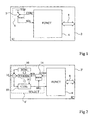
- Figure 1 shows schematically a circuit integrated 2 (IC) intended for a secure application carried by example by a smart card and comprising a functional block 4 (FUNCT) intended to provide a COM control signal to a terminal input of a selection device 6 (SELECT), and for receive a SEL selection signal from the output terminal of the device 6.
- IC circuit integrated 2
- FUNCT functional block 4
- SELECT selection device 6
- Device 6 includes a connected fuse 7 between a supply potential Vdd and the output terminal of the device 6, the fusion of which is controlled by the reception of a COM signal active.
- the environment of circuit 2, connected to block 4 by an input / output port 8, is not shown.
- Block 4 is intended to operate in the mode reserved if it receives an active SEL signal, i.e. as long as fuse 7 is not blown, and in user mode otherwise.
- An equivalent system can also use an anti-fuse which closes a circuit to make a function inactive.
- the COM signal is inactive as long as an operator does not control his activation. Initially, i.e. after manufacturing the circuit, fuse 7 is not blown and block 4 is working in reserved mode. An operator can test and program the block 4 through access 8. Once the test and programming of the block 4 completed, the operator commands block 4 to provide a COM signal active at the input terminal of device 6 to make blow the fuse 7 and lead to a final selection of the user mode.
- Fuse 7 is made in the integrated circuit for prohibit a user from reactivating the mode reserved by a manipulation of signal SEL. Unfortunately, such a fuse can under certain conditions to reform after being melted. We then loses the non-volatile nature of the programming of the state of the SEL signal operated by the fuse.
- ordering the melting of a fuse requires a significant power, which requires block 4 or the device 6 to include power elements. Such elements increase the consumption and the size of the circuit.
- An object of the present invention is to provide a device for selecting the operating mode of a circuit integrated which is permanently lockable and which does not has no problem fuse or anti-fuse like.
- Another object of the present invention is to provide such a device which occupies a reduced surface.
- Another object of the present invention is to provide such a device which has reduced power consumption.
- the present invention also relates to a circuit integrated with such a selection device.
- Another object of the present invention is a method for selecting the operating mode of an integrated circuit such as than implemented by the previous selection device.
- this invention provides a mode selection device operation of an integrated circuit comprising a read only memory storing at least a predetermined value composed of words of data, a controllable non-volatile programmable memory for storing said predetermined value, a comparator indicating how many data words of the value stored in memory programmable are identical to the value data words predetermined, and a control means inactivating a signal operating mode selection when the number of words identical is greater than a predetermined threshold.
- the value stored in the programmable memory varies with the time and the device comprises a writing means for, when the selection signal is inactive, rewrite at intervals regular or not the predetermined value in the memory programmable.
- the writing means is provided for rewriting the value predetermined in the programmable memory at each power-up integrated circuit voltage when the selection signal is inactivated.
- the writing means, the comparator and the control means are implemented in software form by a microprocessor.
- said threshold corresponds to between 70% and 90% of the number of words compared.
- the device includes a functional block intended to operate in a first operating mode when the signal selection is activated and to work in a second operating mode otherwise, the function block to control the programmable memory of store the predetermined value.
- said threshold corresponds to between 70% and 90% of the number of words of the predetermined value.
- the present invention also relates to a method of locking the selected user mode by setting work of the preceding process, consisting in preventing any storage of a value other than the predetermined value in the memory programmable.
- the predetermined value is copied into the programmable memory at least each time the circuit is energized.
- Figure 2 shows schematically a circuit integrated 2 '(IC) comprising a functional block 4 (FUNCT) connected to an environment not represented by an input / output access 8.
- Block 4 is intended to provide a COM signal to a device selection switch 6 '(SELECT) according to the present invention, and for receive a SEL signal from device 6 '.
- the device 6 includes a read only memory 10 (ROM) storing a predetermined value (or code) composed of data words.
- ROM read only memory
- a non-volatile programmable memory 12 for example of FeRAM type, preferably the same size as memory 10, is connected so as to copy the contents of the ROM 10 in response to activation of a WR write signal produced by writing means 14 (WRM).
- WRM writing means 14
- the means 14 is provided for activate the WR signal in response to activation of the COM signal or after energizing the circuit if the SEL signal is inactive.
- a comparator 16 is connected so as to indicate how many words in memory 12 are identical in order and content to words in memory 10.
- a control means 18 connected at the output of comparator 16 produces an active SEL signal as long as the number of identical words is less than a predetermined threshold NT.
- the NT threshold which will be described in more detail below, is preferably less than the total number N of words stored in memory 10.
- a word can be composed of a single bit.
- Block 4 works as before in the mode reserved if it receives an active SEL signal and in user mode if not.
- the COM signal is inactive until an operator not command its activation.
- the memory 12 is such that initially, that is to say after manufacturing the circuit and before all write, it stores an undetermined value. This value indeterminate depends mainly on memory structure 12, and can be evaluated by simulation and confirmed by characterization.
- the NT threshold and the value stored in the memory 10 are chosen so that memories 10 and 12 initially store fewer identical words than threshold NT, so that the control means 18 initially produces an active SEL signal. Block 4 thus works initially in reserved mode.
- the NT threshold preferably corresponds at between 70% and 90% of the word count of the value predetermined.
- an operator can command block 4 to activate the COM signal and thereby copy the predetermined value stored in memory 10 into memory 12. All the words in memory 12 then being identical to those of memory 10, the NT threshold is exceeded and the control means 18 deactivates the signal SEL.
- the connection of memory 12 is such that it is not possible to write to memory 12 a value other than the predetermined value stored in memory 10. The selection of the user mode is definitive, and it is no longer possible to select the mode Reserve.
- a value stored in a memory non-volatile such as memory 12 can vary over time, for example under the effect of radiation.
- the threshold NT is chosen according to the characteristics of the memory 12 so that the number of identical words in memories 10 and 12 remains above the NT threshold despite a small variation in the value stored in memory 12.
- the writing means 14 is provided for rewrite (refresh) the predetermined value in the memory 12, for example each time the circuit is energized when the SEL signal is inactive.
- interval of refreshment for example periodic
- the choice of another interval of refreshment is within the reach of a person skilled in the art depending on the memory 12 used and the application (especially depending on the duration of maintenance under circuit voltage).
- the two intervals are of course combinable.
- the present invention thus makes it possible to use a non-volatile programmable memory with performance of relatively low data retention, which reduces the cost of the device.
- Another advantage of the invention is that the device 6 'occupies a reduced surface and does not require any element of power to blow a possible fuse.
- a selection device has been shown to include writing means, a comparator and a separate control means.
- the present invention also provides in a mode of implementation of the writing means, the comparator and the control means in software form using of a microprocessor.
- ROM can store several predetermined values which are copied together in non-volatile memory.
- the comparator can in this case be provided to determine the number of identical words for each of the values separately.
- the control means is then provided to deactivate the selection signal if the number of identical words is greater than the threshold for each value, or for a predetermined number of values.
- the present invention is capable of various variations and modifications that will appear to humans of career.
- the selection system was shown separate from the integrated circuit functional block, but in practice, it can be integrated into the functional block, in particular in the case of a microprocessor.
- each reserved sub-mode can correspond to a programmable memory value that belongs to a range more or less close to the value of the read only memory, granting the rights of the user, the greater the range close to the value of the read only memory.
- the user mode can be divided into several operating modes, the selection of which may be conventionally controlled by software or by a activation of specific pins.
- the invention has been described in relation to a circuit integrated whose functional block goes into user mode as soon as that the selection signal produced by the selection device is inactive, but the person skilled in the art will easily adapt the present invention to an integrated circuit whose block functional switches to user mode when powered on for the first time voltage following activation of the selection signal.
- the choice of the number and the size of the words stored in the memories as well as the threshold from which considers that there is identity between them is within the reach of the person skilled in the art depending on the application and in particular on the reliability of the non-volatile nature of the programmable memory.
- the threshold is six bits per byte (75%).
- the size of a word in the sense of the invention is then a bit.
Landscapes
- Engineering & Computer Science (AREA)
- Physics & Mathematics (AREA)
- Computer Hardware Design (AREA)
- Theoretical Computer Science (AREA)
- Mathematical Physics (AREA)
- Computer Security & Cryptography (AREA)
- Software Systems (AREA)
- General Engineering & Computer Science (AREA)
- General Physics & Mathematics (AREA)
- Read Only Memory (AREA)
- Semiconductor Integrated Circuits (AREA)
- Storage Device Security (AREA)
Applications Claiming Priority (2)
| Application Number | Priority Date | Filing Date | Title |
|---|---|---|---|
| FR0302230A FR2851668A1 (fr) | 2003-02-24 | 2003-02-24 | Procede et dispositif de selection de mode de fonctionnement d'un circuit integre |
| FR0302230 | 2003-02-24 |
Publications (3)
| Publication Number | Publication Date |
|---|---|
| EP1455259A2 true EP1455259A2 (de) | 2004-09-08 |
| EP1455259A3 EP1455259A3 (de) | 2004-09-29 |
| EP1455259B1 EP1455259B1 (de) | 2010-12-01 |
Family
ID=32799531
Family Applications (1)
| Application Number | Title | Priority Date | Filing Date |
|---|---|---|---|
| EP04300094A Expired - Lifetime EP1455259B1 (de) | 2003-02-24 | 2004-02-23 | Methode und Apparat zum Auswählen eines Schaltkreis Betriebsmodus |
Country Status (5)
| Country | Link |
|---|---|
| US (1) | US7194570B2 (de) |
| EP (1) | EP1455259B1 (de) |
| JP (1) | JP2004259272A (de) |
| DE (1) | DE602004030295D1 (de) |
| FR (1) | FR2851668A1 (de) |
Citations (2)
| Publication number | Priority date | Publication date | Assignee | Title |
|---|---|---|---|---|
| EP0610886A2 (de) | 1993-02-09 | 1994-08-17 | Mitsubishi Denki Kabushiki Kaisha | Mikrorechner für IC-Karte |
| US5826007A (en) | 1996-01-22 | 1998-10-20 | Kabushiki Kaisha Toshiba | Memory data protection circuit |
Family Cites Families (11)
| Publication number | Priority date | Publication date | Assignee | Title |
|---|---|---|---|---|
| GB8511995D0 (en) * | 1985-05-11 | 1985-06-19 | Ross S R | Software protection |
| JPH0827730B2 (ja) * | 1986-11-07 | 1996-03-21 | 沖電気工業株式会社 | シングルチップマイクロコンピュータ及びそのテスト方法 |
| US5602789A (en) * | 1991-03-12 | 1997-02-11 | Kabushiki Kaisha Toshiba | Electrically erasable and programmable non-volatile and multi-level memory systemn with write-verify controller |
| DE69229521T2 (de) * | 1991-04-25 | 2000-03-30 | Nippon Steel Corp | Datenbankauffindungssystem |
| KR0140176B1 (ko) * | 1994-11-30 | 1998-07-15 | 김광호 | 반도체 메모리장치의 동작모드 제어장치 및 방법 |
| JP3351953B2 (ja) * | 1996-03-19 | 2002-12-03 | 富士通株式会社 | モードレジスタ制御回路およびこれを有する半導体装置 |
| JPH10302482A (ja) * | 1997-02-27 | 1998-11-13 | Sanyo Electric Co Ltd | 半導体メモリ |
| US6762951B2 (en) * | 2001-11-13 | 2004-07-13 | Hitachi, Ltd. | Semiconductor integrated circuit device |
| EP1115164B1 (de) * | 2000-01-07 | 2005-05-25 | Sharp Kabushiki Kaisha | Magnetoresistive Anordnung und diese verwendendes magnetisches Speicherelement |
| DE10106340A1 (de) * | 2001-02-09 | 2002-08-29 | Europ Lab Molekularbiolog | Schaltung zur Verarbeitung von Daten |
| US6989861B2 (en) * | 2001-09-14 | 2006-01-24 | Hewlett-Packard Development Company, L.P. | User selection of power-on configuration |
-
2003
- 2003-02-24 FR FR0302230A patent/FR2851668A1/fr not_active Withdrawn
-
2004
- 2004-02-23 JP JP2004046082A patent/JP2004259272A/ja not_active Withdrawn
- 2004-02-23 DE DE602004030295T patent/DE602004030295D1/de not_active Expired - Lifetime
- 2004-02-23 EP EP04300094A patent/EP1455259B1/de not_active Expired - Lifetime
- 2004-02-23 US US10/784,430 patent/US7194570B2/en not_active Expired - Fee Related
Patent Citations (2)
| Publication number | Priority date | Publication date | Assignee | Title |
|---|---|---|---|---|
| EP0610886A2 (de) | 1993-02-09 | 1994-08-17 | Mitsubishi Denki Kabushiki Kaisha | Mikrorechner für IC-Karte |
| US5826007A (en) | 1996-01-22 | 1998-10-20 | Kabushiki Kaisha Toshiba | Memory data protection circuit |
Also Published As
| Publication number | Publication date |
|---|---|
| EP1455259B1 (de) | 2010-12-01 |
| EP1455259A3 (de) | 2004-09-29 |
| FR2851668A1 (fr) | 2004-08-27 |
| US7194570B2 (en) | 2007-03-20 |
| DE602004030295D1 (de) | 2011-01-13 |
| JP2004259272A (ja) | 2004-09-16 |
| US20040165458A1 (en) | 2004-08-26 |
Similar Documents
| Publication | Publication Date | Title |
|---|---|---|
| EP0918336B1 (de) | Elektrisch programmier- und löschbarer nichtflüchtiger Speicher mit einem lese- und/oder schreibgeschützen Bereich einschliesslich zugehöriger elektronischer Schaltung | |
| EP0437386B1 (de) | Sicherheitsverriegelung für integrierten Schaltkreis | |
| EP0377368B1 (de) | Datenverarbeitungsanlage mit einem nichtflüchtigen und elektrisch löschbaren und umprogrammierbaren Speicher | |
| EP0554164B1 (de) | Chipkarte mit mehreren Kommunikationsprotokollen | |
| EP0432049B1 (de) | MOS als Sicherung bei programmierbarer Durchbrennung eines Tunneloxydes | |
| EP0317014A1 (de) | Direktzugriffsspeichereinheit mit mehreren Testbetriebsarten und Rechner, ausgerüstet mit solchen Einheiten | |
| EP0318363A1 (de) | Verfahren zum Testen von Zellen von elektrisch programmierbaren Speichern und entsprechende integrierte Schaltung | |
| FR2711833A1 (fr) | Circuit intégré contenant une mémoire protégée et système sécurisé utilisant ledit circuit intégré. | |
| EP0669576A1 (de) | Speicherredundanzschaltung | |
| EP1359550A1 (de) | Wiederherstellung einer Geheimzahl mittels der Kennzahl einer integrierten Schaltung | |
| EP0575480B1 (de) | Verfahren zum programmieren eines integrierten speichers, besonders für speicherkarten | |
| EP1455259B1 (de) | Methode und Apparat zum Auswählen eines Schaltkreis Betriebsmodus | |
| EP0718769A1 (de) | Speicherwörterzugangsschutzvorrichtung | |
| FR2723794A1 (fr) | Micro-ordinateur comprenant une memoire eprom et procede de fabrication de celui-ci | |
| EP0665559A1 (de) | Nichtflüchtiger programmierbarer Flip-Flop mit Verminderung von parasitären Effekten beim Lesen für Speicherredundanzschaltung | |
| EP0272977B1 (de) | Schutzvorrichtung für einen lösch- und neuprogrammierbaren Festwertspeicher | |
| EP1467313B1 (de) | Verfahren und Vorrichtung zur Auswahl der Betriebsart einer Integrierten Schaltung | |
| EP0267091B1 (de) | Elektrisch programmierbarer Festwertspeicher | |
| EP1476878A2 (de) | Zerstörungsfreie einmal programmierbare speicherzelle | |
| EP1476879A2 (de) | Einmal programmierbare speicherzelle | |
| EP1217628A1 (de) | Verfahren und System zum Einstellen eines Taktsignals oder anderer Eigenschaften einer integrierten Schaltungsanordnung sowie entsprechende integrierte Schaltungsanordnung | |
| EP1202181A1 (de) | Zugriffssteuerung zu einem integrierten Speicher mit einem Mikroprozessor | |
| FR2846463A1 (fr) | Compteur monotone a base de cellules memoire | |
| EP0734023A1 (de) | Schreibschutzverfahren und integrierte Schaltung eines Speichers in einer integrierten Schaltung | |
| EP0996064A1 (de) | Einmalig programmierbare Speicherzelle |
Legal Events
| Date | Code | Title | Description |
|---|---|---|---|
| PUAI | Public reference made under article 153(3) epc to a published international application that has entered the european phase |
Free format text: ORIGINAL CODE: 0009012 |
|
| PUAL | Search report despatched |
Free format text: ORIGINAL CODE: 0009013 |
|
| AK | Designated contracting states |
Kind code of ref document: A2 Designated state(s): AT BE BG CH CY CZ DE DK EE ES FI FR GB GR HU IE IT LI LU MC NL PT RO SE SI SK TR |
|
| AX | Request for extension of the european patent |
Extension state: AL LT LV MK |
|
| AK | Designated contracting states |
Kind code of ref document: A3 Designated state(s): AT BE BG CH CY CZ DE DK EE ES FI FR GB GR HU IE IT LI LU MC NL PT RO SE SI SK TR |
|
| AX | Request for extension of the european patent |
Extension state: AL LT LV MK |
|
| 17P | Request for examination filed |
Effective date: 20050325 |
|
| AKX | Designation fees paid |
Designated state(s): DE FR GB IT |
|
| 17Q | First examination report despatched |
Effective date: 20080124 |
|
| GRAP | Despatch of communication of intention to grant a patent |
Free format text: ORIGINAL CODE: EPIDOSNIGR1 |
|
| RIC1 | Information provided on ipc code assigned before grant |
Ipc: G06F 21/02 20060101AFI20100416BHEP |
|
| GRAC | Information related to communication of intention to grant a patent modified |
Free format text: ORIGINAL CODE: EPIDOSCIGR1 |
|
| GRAS | Grant fee paid |
Free format text: ORIGINAL CODE: EPIDOSNIGR3 |
|
| GRAA | (expected) grant |
Free format text: ORIGINAL CODE: 0009210 |
|
| AK | Designated contracting states |
Kind code of ref document: B1 Designated state(s): DE FR GB IT |
|
| REG | Reference to a national code |
Ref country code: GB Ref legal event code: FG4D Free format text: NOT ENGLISH |
|
| REF | Corresponds to: |
Ref document number: 602004030295 Country of ref document: DE Date of ref document: 20110113 Kind code of ref document: P |
|
| PGFP | Annual fee paid to national office [announced via postgrant information from national office to epo] |
Ref country code: DE Payment date: 20110207 Year of fee payment: 8 Ref country code: IT Payment date: 20110122 Year of fee payment: 8 Ref country code: FR Payment date: 20110311 Year of fee payment: 8 |
|
| PGFP | Annual fee paid to national office [announced via postgrant information from national office to epo] |
Ref country code: GB Payment date: 20110128 Year of fee payment: 8 |
|
| PLBE | No opposition filed within time limit |
Free format text: ORIGINAL CODE: 0009261 |
|
| STAA | Information on the status of an ep patent application or granted ep patent |
Free format text: STATUS: NO OPPOSITION FILED WITHIN TIME LIMIT |
|
| 26N | No opposition filed |
Effective date: 20110902 |
|
| REG | Reference to a national code |
Ref country code: DE Ref legal event code: R097 Ref document number: 602004030295 Country of ref document: DE Effective date: 20110902 |
|
| GBPC | Gb: european patent ceased through non-payment of renewal fee |
Effective date: 20120223 |
|
| REG | Reference to a national code |
Ref country code: FR Ref legal event code: ST Effective date: 20121031 |
|
| PG25 | Lapsed in a contracting state [announced via postgrant information from national office to epo] |
Ref country code: IT Free format text: LAPSE BECAUSE OF NON-PAYMENT OF DUE FEES Effective date: 20120223 |
|
| REG | Reference to a national code |
Ref country code: DE Ref legal event code: R119 Ref document number: 602004030295 Country of ref document: DE Effective date: 20120901 |
|
| PG25 | Lapsed in a contracting state [announced via postgrant information from national office to epo] |
Ref country code: GB Free format text: LAPSE BECAUSE OF NON-PAYMENT OF DUE FEES Effective date: 20120223 Ref country code: FR Free format text: LAPSE BECAUSE OF NON-PAYMENT OF DUE FEES Effective date: 20120229 |
|
| PG25 | Lapsed in a contracting state [announced via postgrant information from national office to epo] |
Ref country code: DE Free format text: LAPSE BECAUSE OF NON-PAYMENT OF DUE FEES Effective date: 20120901 |