EP1453100B1 - Bildaufnahmevorrichtungsstruktur - Google Patents
Bildaufnahmevorrichtungsstruktur Download PDFInfo
- Publication number
- EP1453100B1 EP1453100B1 EP03251149A EP03251149A EP1453100B1 EP 1453100 B1 EP1453100 B1 EP 1453100B1 EP 03251149 A EP03251149 A EP 03251149A EP 03251149 A EP03251149 A EP 03251149A EP 1453100 B1 EP1453100 B1 EP 1453100B1
- Authority
- EP
- European Patent Office
- Prior art keywords
- well
- image sensing
- sensing structure
- sti
- photodiode
- Prior art date
- Legal status (The legal status is an assumption and is not a legal conclusion. Google has not performed a legal analysis and makes no representation as to the accuracy of the status listed.)
- Expired - Lifetime
Links
- 238000002955 isolation Methods 0.000 claims description 3
- 238000000034 method Methods 0.000 description 9
- 239000007943 implant Substances 0.000 description 6
- 238000004519 manufacturing process Methods 0.000 description 5
- 238000002513 implantation Methods 0.000 description 4
- 230000035945 sensitivity Effects 0.000 description 4
- 239000000758 substrate Substances 0.000 description 4
- XUIMIQQOPSSXEZ-UHFFFAOYSA-N Silicon Chemical compound [Si] XUIMIQQOPSSXEZ-UHFFFAOYSA-N 0.000 description 3
- 238000005516 engineering process Methods 0.000 description 3
- 230000008569 process Effects 0.000 description 3
- 238000003384 imaging method Methods 0.000 description 2
- 230000004048 modification Effects 0.000 description 2
- 238000012986 modification Methods 0.000 description 2
- 229910052710 silicon Inorganic materials 0.000 description 2
- 239000010703 silicon Substances 0.000 description 2
- 241000699670 Mus sp. Species 0.000 description 1
- 230000001668 ameliorated effect Effects 0.000 description 1
- 230000004888 barrier function Effects 0.000 description 1
- 230000008901 benefit Effects 0.000 description 1
- 238000006243 chemical reaction Methods 0.000 description 1
- 239000004020 conductor Substances 0.000 description 1
- 230000001419 dependent effect Effects 0.000 description 1
- 238000005530 etching Methods 0.000 description 1
- 230000006872 improvement Effects 0.000 description 1
- 239000000463 material Substances 0.000 description 1
- 230000003287 optical effect Effects 0.000 description 1
- 229910021420 polycrystalline silicon Inorganic materials 0.000 description 1
- 229920005591 polysilicon Polymers 0.000 description 1
- 230000004044 response Effects 0.000 description 1
- 239000004065 semiconductor Substances 0.000 description 1
- 239000007787 solid Substances 0.000 description 1
Images

Classifications
-
- H—ELECTRICITY
- H10—SEMICONDUCTOR DEVICES; ELECTRIC SOLID-STATE DEVICES NOT OTHERWISE PROVIDED FOR
- H10F—INORGANIC SEMICONDUCTOR DEVICES SENSITIVE TO INFRARED RADIATION, LIGHT, ELECTROMAGNETIC RADIATION OF SHORTER WAVELENGTH OR CORPUSCULAR RADIATION
- H10F39/00—Integrated devices, or assemblies of multiple devices, comprising at least one element covered by group H10F30/00, e.g. radiation detectors comprising photodiode arrays
- H10F39/10—Integrated devices
- H10F39/103—Integrated devices the at least one element covered by H10F30/00 having potential barriers, e.g. integrated devices comprising photodiodes or phototransistors
-
- H—ELECTRICITY
- H10—SEMICONDUCTOR DEVICES; ELECTRIC SOLID-STATE DEVICES NOT OTHERWISE PROVIDED FOR
- H10F—INORGANIC SEMICONDUCTOR DEVICES SENSITIVE TO INFRARED RADIATION, LIGHT, ELECTROMAGNETIC RADIATION OF SHORTER WAVELENGTH OR CORPUSCULAR RADIATION
- H10F39/00—Integrated devices, or assemblies of multiple devices, comprising at least one element covered by group H10F30/00, e.g. radiation detectors comprising photodiode arrays
- H10F39/80—Constructional details of image sensors
- H10F39/803—Pixels having integrated switching, control, storage or amplification elements
Definitions
- the present invention relates to an image sensing structure, and in particular but not exclusively to an image sensing structure comprising a photodiode that provides highly accurate matching between pixels.
- transistor fabrication multiple transistors of similar conductivity types are commonly located in a single well.
- the well In normal use, the well is reverse biased with respect to the transistor and the substrate and there is virtually no current flowing into or out of the well and transistor. The transistors therefore do not interact, and so the electrical properties of the well are usually ignored.
- FPN Fixed Pattern Noise
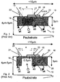
- Fig. 1 shows a common form of CMOS image sensing structure.
- An epitaxial layer 10 is formed on a P substrate 12.
- a photodiode comprising an N-well collection node 14 with surrounding P-wells 16 is formed in the epitaxial layer 10.
- the collection node 14 has a conductor 18 attached which carries a signal to a transistor 20, which is part of readout electronics.
- the photodiode illustrated in Fig. 1 is a relatively small photodiode, having a width of less than ten micrometers. Typically, such a photodiode will have a width of between four and six micrometers. As also illustrated in Fig. 1 , the epitaxial layer 10 has a depth of between four and five ⁇ m, and both the N-well and P-wells have a depth of three ⁇ m, as measured from the upper surface of the epitaxial layer 10.
- a problem with this technique is that well implantation is not a critical parameter for CMOS transistors and hence is not particularly well controlled.
- the width of the collection node 14, shown by X in Fig. 1 varies from part to part and pixel to pixel, by a typical variation dX.
- the value of dX for the photodiode of Fig. 1 is typically ⁇ 300 nm. This variation in the width of the collection node 14 causes variation in the capacitance of the photodiode, leading to the abovementioned problem of mismatch between pixels.
- Fig. 2 shows a modification that can be made to the structure of Fig. 1 .
- an N+ implant is used as the collection node.
- N+ is used to construct a transistor 26, and its implantation is very well controlled.
- the part to part and pixel to pixel variation, represented by dX2, in the photodiode of Fig. 2 typically has a value of ⁇ 100 nm.
- Fig. 3 shows an arrangement, not forming part of the present invention, which provides a deep yet accurate implant
- CMOS technologies use a technique called Shallow Trench Isolation (STI) to control accurately the width of (active) N+ or P+ areas
- STI Shallow Trench Isolation
- Photo-resist is patterned outside the active areas.
- Anisotropic etching is used to etch a deep (typically 2 ⁇ m) trench. This provides a well defined edge for the implants. After implant, polysilicon is deposited inside the trenches.
- the present invention provides STI 30 around the collection node 28 in order to provide better control of the width, X, of the collection node 28.
- the N-well collection node 28 and the surrounding P-wells 16 have a depth of 3 ⁇ m below the upper surface of the epitaxial layer 10, and the STI has a depth of 2 ⁇ m.
- the STI is formed prior to implantation of the N-well, thus providing a definite border for the p-n junction to increase control of collection node 28 width X, with a typical value for dX3 being ⁇ 50 nm.
- This technique combines the advantage of a deep N-well for better quantum efficiency with better control of implantation and hence capacitance. As dX3 ⁇ dX1 we get much better matching than N-Well implant photodiodes.
- the STI would be as deep, or deeper as the N-Well, as the p-n junction below the STI is a diffuse barrier.
- STI is usually formed at a depth of 2 ⁇ m, as this is all that is required for transistors. In this situation, two thirds of the diode's capacitance is controlled accurately, which represents an improvement over prior art.
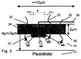
- Fig. 4 illustrates an embodiment of the present invention, which is applicable for relatively large photodiodes, having widths equal to or greater than ten micrometers. Typically, large photodiodes will have widths between forty and sixty ⁇ m.
- An N-well collection node 32 is bounded by STI 34. To increase sensitivity, the P-well 16 that is shown in Figs. 1-3 is replaced by P-Epi. This means that all the electrons e 1-e4 will most likely be collected by the collection node 32.
Landscapes
- Solid State Image Pick-Up Elements (AREA)
- Light Receiving Elements (AREA)
Claims (6)
- Eine Bildabtastkonstruktion, die eine Photodiode mit einer ersten Wanne (32) einer ersten Leitfähigkeitsart, die geeignet ist, um als ein Sammelknoten zu wirken, und die in einer Schicht (10) einer zweiten Leitfähigkeitsart gebildet ist, beinhaltet, wobei mindestens ein oberer Abschnitt der ersten Wanne (32) von einer flachen Grabenisolation (STI) (34) an mindestens einem Teil ihres horizontal begrenzten Umfangs eingegrenzt wird, dadurch gekennzeichnet, dass die Schicht (10) lediglich eine epitaktische Schicht ohne Wannen der zweiten Leitfähigkeitsart beinhaltet.
- Bildabtastkonstruktion gemäß Anspruch 1, wobei mindestens ein oberer Abschnitt der ersten Wanne (32) von STI (34) an der Gesamtheit ihres horizontal begrenzten Umfangs eingegrenzt wird.
- Bildabtastkonstruktion gemäß einem der vorhergehenden Ansprüche, wobei die erste Wanne (32) eine N-Wanne beinhaltet und die Schicht (10) der zweiten Leitfähigkeitsart P-epitaktisch ist.
- Bildabtastkonstruktion gemäß Anspruch 3, wobei an der Schnittstelle zwischen der STI (34) und der ersten Wanne (32) ein NP-Übergang gebildet ist.
- Bildabtastkonstruktion gemäß einem der vorhergehenden Ansprüche, wobei die Photodiode eine Breite von oder größer als zehn Mikrometer(n) aufweist.
- Bildabtastkonstruktion gemäß Anspruch 5, wobei die erste Wanne (32) eine Tiefe von ungefähr 3 µm aufweist und die STI (34) eine Tiefe von ungefähr 2 µm aufweist.
Priority Applications (3)
| Application Number | Priority Date | Filing Date | Title |
|---|---|---|---|
| EP03251149A EP1453100B1 (de) | 2003-02-26 | 2003-02-26 | Bildaufnahmevorrichtungsstruktur |
| DE60324092T DE60324092D1 (de) | 2003-02-26 | 2003-02-26 | Bildaufnahmevorrichtungsstruktur |
| US10/786,878 US7288801B2 (en) | 2003-02-26 | 2004-02-25 | Image sensing structure |
Applications Claiming Priority (1)
| Application Number | Priority Date | Filing Date | Title |
|---|---|---|---|
| EP03251149A EP1453100B1 (de) | 2003-02-26 | 2003-02-26 | Bildaufnahmevorrichtungsstruktur |
Publications (2)
| Publication Number | Publication Date |
|---|---|
| EP1453100A1 EP1453100A1 (de) | 2004-09-01 |
| EP1453100B1 true EP1453100B1 (de) | 2008-10-15 |
Family
ID=32748968
Family Applications (1)
| Application Number | Title | Priority Date | Filing Date |
|---|---|---|---|
| EP03251149A Expired - Lifetime EP1453100B1 (de) | 2003-02-26 | 2003-02-26 | Bildaufnahmevorrichtungsstruktur |
Country Status (3)
| Country | Link |
|---|---|
| US (1) | US7288801B2 (de) |
| EP (1) | EP1453100B1 (de) |
| DE (1) | DE60324092D1 (de) |
Families Citing this family (4)
| Publication number | Priority date | Publication date | Assignee | Title |
|---|---|---|---|---|
| EP1665382B1 (de) * | 2003-09-18 | 2012-12-12 | iC-Haus GmbH | Optoelektronischer sensor und vorrichtung zur 3d-abstandsmessung |
| CN100459141C (zh) * | 2004-07-07 | 2009-02-04 | 松下电器产业株式会社 | 固体摄像装置、其制造方法及使用它的摄像机 |
| EP1865556B1 (de) | 2006-06-05 | 2010-11-17 | STMicroelectronics Srl | DELTA E-E-Strahlungsdetektor mit Isolationsgräben und seine Herstellungsmethode |
| US8008695B2 (en) * | 2008-05-29 | 2011-08-30 | Omnivision Technologies, Inc. | Image sensor with backside passivation and metal layer |
Family Cites Families (7)
| Publication number | Priority date | Publication date | Assignee | Title |
|---|---|---|---|---|
| US6140156A (en) * | 1999-07-13 | 2000-10-31 | United Microelectronics Corp. | Fabrication method of isolation structure photodiode |
| JP3884600B2 (ja) * | 1999-11-29 | 2007-02-21 | 富士通株式会社 | 光電変換装置及びその製造方法 |
| US6407440B1 (en) * | 2000-02-25 | 2002-06-18 | Micron Technology Inc. | Pixel cell with high storage capacitance for a CMOS imager |
| KR20020002499A (ko) * | 2000-03-09 | 2002-01-09 | 롤페스 요하네스 게라투스 알베르투스 | 카메라 시스템, 카메라 시스템 제조 방법, 카메라 시스템동작 방법 및 집적 회로 |
| US6512280B2 (en) * | 2001-05-16 | 2003-01-28 | Texas Instruments Incorporated | Integrated CMOS structure for gate-controlled buried photodiode |
| TW483176B (en) * | 2001-05-31 | 2002-04-11 | United Microelectronics Corp | Method for decreasing leakage current of photodiode |
| US6504196B1 (en) * | 2001-08-30 | 2003-01-07 | Micron Technology, Inc. | CMOS imager and method of formation |
-
2003
- 2003-02-26 EP EP03251149A patent/EP1453100B1/de not_active Expired - Lifetime
- 2003-02-26 DE DE60324092T patent/DE60324092D1/de not_active Expired - Lifetime
-
2004
- 2004-02-25 US US10/786,878 patent/US7288801B2/en not_active Expired - Lifetime
Also Published As
| Publication number | Publication date |
|---|---|
| DE60324092D1 (de) | 2008-11-27 |
| US20040217359A1 (en) | 2004-11-04 |
| US7288801B2 (en) | 2007-10-30 |
| EP1453100A1 (de) | 2004-09-01 |
Similar Documents
| Publication | Publication Date | Title |
|---|---|---|
| EP1032049B1 (de) | Photoelektrisches Umwandlungselement | |
| US6423993B1 (en) | Solid-state image-sensing device and method for producing the same | |
| EP2487714B1 (de) | Halbleiterelement und festkörperbildaufnahmevorrichtung | |
| US8048711B2 (en) | Method for forming deep isolation in imagers | |
| US6545302B2 (en) | Image sensor capable of decreasing leakage current between diodes and method for fabricating the same | |
| JP3584196B2 (ja) | 受光素子及びそれを有する光電変換装置 | |
| US9620545B2 (en) | Solid-state image pickup device and method for producing the same | |
| JP5442100B2 (ja) | 光電変換装置の製造方法 | |
| US20100109060A1 (en) | Image sensor with backside photodiode implant | |
| EP2282345A2 (de) | Bildsensor mit einem Übertragungsgate mit mehreren Kanalunterregionen | |
| KR20000044627A (ko) | 칼라이미지 센서 및 그 제조방법 | |
| US20100140668A1 (en) | Shallow trench isolation regions in image sensors | |
| US20100148230A1 (en) | Trench isolation regions in image sensors | |
| JP2004312039A (ja) | 光電変換素子 | |
| CN114975493A (zh) | 用于先进cmos图像传感器的倾斜转移栅极 | |
| EP1453100A1 (de) | Bildaufnahmevorrichtungsstruktur | |
| JP4387978B2 (ja) | 光電変換装置及び撮像システム | |
| JP2002329856A (ja) | 光電変換装置及びその製造方法 | |
| KR100788483B1 (ko) | 이미지 센서의 픽셀 구조 및 그 제조 방법 | |
| CN101203959A (zh) | 图像传感器像素及其制造方法 | |
| KR20050079436A (ko) | 화소간 신호왜곡을 개선한 이미지 센서 및 그 제조방법 | |
| DE102005051485B4 (de) | Bildsensorbauelement und Herstellungsverfahren | |
| KR19990047734A (ko) | 고체 촬상 소자의 제조 방법 |
Legal Events
| Date | Code | Title | Description |
|---|---|---|---|
| PUAI | Public reference made under article 153(3) epc to a published international application that has entered the european phase |
Free format text: ORIGINAL CODE: 0009012 |
|
| AK | Designated contracting states |
Kind code of ref document: A1 Designated state(s): AT BE BG CH CY CZ DE DK EE ES FI FR GB GR HU IE IT LI LU MC NL PT SE SI SK TR |
|
| AX | Request for extension of the european patent |
Extension state: AL LT LV MK RO |
|
| 17P | Request for examination filed |
Effective date: 20050215 |
|
| AKX | Designation fees paid |
Designated state(s): DE FR GB IT |
|
| 17Q | First examination report despatched |
Effective date: 20071220 |
|
| GRAP | Despatch of communication of intention to grant a patent |
Free format text: ORIGINAL CODE: EPIDOSNIGR1 |
|
| GRAS | Grant fee paid |
Free format text: ORIGINAL CODE: EPIDOSNIGR3 |
|
| GRAA | (expected) grant |
Free format text: ORIGINAL CODE: 0009210 |
|
| AK | Designated contracting states |
Kind code of ref document: B1 Designated state(s): DE FR GB IT |
|
| REG | Reference to a national code |
Ref country code: GB Ref legal event code: FG4D |
|
| RAP2 | Party data changed (patent owner data changed or rights of a patent transferred) |
Owner name: STMICROELECTRONICS (RESEARCH & DEVELOPMENT) LIMITE |
|
| REF | Corresponds to: |
Ref document number: 60324092 Country of ref document: DE Date of ref document: 20081127 Kind code of ref document: P |
|
| PLBE | No opposition filed within time limit |
Free format text: ORIGINAL CODE: 0009261 |
|
| STAA | Information on the status of an ep patent application or granted ep patent |
Free format text: STATUS: NO OPPOSITION FILED WITHIN TIME LIMIT |
|
| PG25 | Lapsed in a contracting state [announced via postgrant information from national office to epo] |
Ref country code: IT Free format text: LAPSE BECAUSE OF FAILURE TO SUBMIT A TRANSLATION OF THE DESCRIPTION OR TO PAY THE FEE WITHIN THE PRESCRIBED TIME-LIMIT Effective date: 20081015 |
|
| 26N | No opposition filed |
Effective date: 20090716 |
|
| PGFP | Annual fee paid to national office [announced via postgrant information from national office to epo] |
Ref country code: FR Payment date: 20110311 Year of fee payment: 9 |
|
| PGFP | Annual fee paid to national office [announced via postgrant information from national office to epo] |
Ref country code: GB Payment date: 20110128 Year of fee payment: 9 |
|
| GBPC | Gb: european patent ceased through non-payment of renewal fee |
Effective date: 20120226 |
|
| REG | Reference to a national code |
Ref country code: FR Ref legal event code: ST Effective date: 20121031 |
|
| PG25 | Lapsed in a contracting state [announced via postgrant information from national office to epo] |
Ref country code: FR Free format text: LAPSE BECAUSE OF NON-PAYMENT OF DUE FEES Effective date: 20120229 Ref country code: GB Free format text: LAPSE BECAUSE OF NON-PAYMENT OF DUE FEES Effective date: 20120226 |
|
| PGFP | Annual fee paid to national office [announced via postgrant information from national office to epo] |
Ref country code: DE Payment date: 20220119 Year of fee payment: 20 |
|
| REG | Reference to a national code |
Ref country code: DE Ref legal event code: R071 Ref document number: 60324092 Country of ref document: DE |