EP1447839B1 - Semiconductor substrate, field-effect transistor and their manufacturing methods - Google Patents
Semiconductor substrate, field-effect transistor and their manufacturing methods Download PDFInfo
- Publication number
- EP1447839B1 EP1447839B1 EP02755785.9A EP02755785A EP1447839B1 EP 1447839 B1 EP1447839 B1 EP 1447839B1 EP 02755785 A EP02755785 A EP 02755785A EP 1447839 B1 EP1447839 B1 EP 1447839B1
- Authority
- EP
- European Patent Office
- Prior art keywords
- layer
- sige layer
- sige
- composition ratio
- composition
- Prior art date
- Legal status (The legal status is an assumption and is not a legal conclusion. Google has not performed a legal analysis and makes no representation as to the accuracy of the status listed.)
- Expired - Lifetime
Links
Images










Classifications
-
- H—ELECTRICITY
- H10—SEMICONDUCTOR DEVICES; ELECTRIC SOLID-STATE DEVICES NOT OTHERWISE PROVIDED FOR
- H10D—INORGANIC ELECTRIC SEMICONDUCTOR DEVICES
- H10D30/00—Field-effect transistors [FET]
- H10D30/80—FETs having rectifying junction gate electrodes
- H10D30/801—FETs having heterojunction gate electrodes
-
- H—ELECTRICITY
- H10—SEMICONDUCTOR DEVICES; ELECTRIC SOLID-STATE DEVICES NOT OTHERWISE PROVIDED FOR
- H10P—GENERIC PROCESSES OR APPARATUS FOR THE MANUFACTURE OR TREATMENT OF DEVICES COVERED BY CLASS H10
- H10P10/00—Bonding of wafers, substrates or parts of devices
-
- H—ELECTRICITY
- H10—SEMICONDUCTOR DEVICES; ELECTRIC SOLID-STATE DEVICES NOT OTHERWISE PROVIDED FOR
- H10D—INORGANIC ELECTRIC SEMICONDUCTOR DEVICES
- H10D30/00—Field-effect transistors [FET]
- H10D30/60—Insulated-gate field-effect transistors [IGFET]
- H10D30/751—Insulated-gate field-effect transistors [IGFET] having composition variations in the channel regions
-
- H—ELECTRICITY
- H10—SEMICONDUCTOR DEVICES; ELECTRIC SOLID-STATE DEVICES NOT OTHERWISE PROVIDED FOR
- H10D—INORGANIC ELECTRIC SEMICONDUCTOR DEVICES
- H10D30/00—Field-effect transistors [FET]
- H10D30/60—Insulated-gate field-effect transistors [IGFET]
- H10D30/791—Arrangements for exerting mechanical stress on the crystal lattice of the channel regions
- H10D30/798—Arrangements for exerting mechanical stress on the crystal lattice of the channel regions being provided in or under the channel regions
-
- H—ELECTRICITY
- H10—SEMICONDUCTOR DEVICES; ELECTRIC SOLID-STATE DEVICES NOT OTHERWISE PROVIDED FOR
- H10P—GENERIC PROCESSES OR APPARATUS FOR THE MANUFACTURE OR TREATMENT OF DEVICES COVERED BY CLASS H10
- H10P14/00—Formation of materials, e.g. in the shape of layers or pillars
- H10P14/20—Formation of materials, e.g. in the shape of layers or pillars of semiconductor materials
- H10P14/29—Formation of materials, e.g. in the shape of layers or pillars of semiconductor materials characterised by the substrates
- H10P14/2901—Materials
- H10P14/2902—Materials being Group IVA materials
- H10P14/2905—Silicon, silicon germanium or germanium
-
- H—ELECTRICITY
- H10—SEMICONDUCTOR DEVICES; ELECTRIC SOLID-STATE DEVICES NOT OTHERWISE PROVIDED FOR
- H10P—GENERIC PROCESSES OR APPARATUS FOR THE MANUFACTURE OR TREATMENT OF DEVICES COVERED BY CLASS H10
- H10P14/00—Formation of materials, e.g. in the shape of layers or pillars
- H10P14/20—Formation of materials, e.g. in the shape of layers or pillars of semiconductor materials
- H10P14/32—Formation of materials, e.g. in the shape of layers or pillars of semiconductor materials characterised by intermediate layers between substrates and deposited layers
- H10P14/3202—Materials thereof
- H10P14/3204—Materials thereof being Group IVA semiconducting materials
- H10P14/3211—Silicon, silicon germanium or germanium
-
- H—ELECTRICITY
- H10—SEMICONDUCTOR DEVICES; ELECTRIC SOLID-STATE DEVICES NOT OTHERWISE PROVIDED FOR
- H10P—GENERIC PROCESSES OR APPARATUS FOR THE MANUFACTURE OR TREATMENT OF DEVICES COVERED BY CLASS H10
- H10P14/00—Formation of materials, e.g. in the shape of layers or pillars
- H10P14/20—Formation of materials, e.g. in the shape of layers or pillars of semiconductor materials
- H10P14/32—Formation of materials, e.g. in the shape of layers or pillars of semiconductor materials characterised by intermediate layers between substrates and deposited layers
- H10P14/3242—Structure
- H10P14/3244—Layer structure
- H10P14/3248—Layer structure consisting of two layers
-
- H—ELECTRICITY
- H10—SEMICONDUCTOR DEVICES; ELECTRIC SOLID-STATE DEVICES NOT OTHERWISE PROVIDED FOR
- H10P—GENERIC PROCESSES OR APPARATUS FOR THE MANUFACTURE OR TREATMENT OF DEVICES COVERED BY CLASS H10
- H10P14/00—Formation of materials, e.g. in the shape of layers or pillars
- H10P14/20—Formation of materials, e.g. in the shape of layers or pillars of semiconductor materials
- H10P14/32—Formation of materials, e.g. in the shape of layers or pillars of semiconductor materials characterised by intermediate layers between substrates and deposited layers
- H10P14/3242—Structure
- H10P14/3244—Layer structure
- H10P14/3251—Layer structure consisting of three or more layers
-
- H—ELECTRICITY
- H10—SEMICONDUCTOR DEVICES; ELECTRIC SOLID-STATE DEVICES NOT OTHERWISE PROVIDED FOR
- H10P—GENERIC PROCESSES OR APPARATUS FOR THE MANUFACTURE OR TREATMENT OF DEVICES COVERED BY CLASS H10
- H10P14/00—Formation of materials, e.g. in the shape of layers or pillars
- H10P14/20—Formation of materials, e.g. in the shape of layers or pillars of semiconductor materials
- H10P14/32—Formation of materials, e.g. in the shape of layers or pillars of semiconductor materials characterised by intermediate layers between substrates and deposited layers
- H10P14/3242—Structure
- H10P14/3244—Layer structure
- H10P14/3251—Layer structure consisting of three or more layers
- H10P14/3252—Alternating layers, e.g. superlattice
-
- H—ELECTRICITY
- H10—SEMICONDUCTOR DEVICES; ELECTRIC SOLID-STATE DEVICES NOT OTHERWISE PROVIDED FOR
- H10P—GENERIC PROCESSES OR APPARATUS FOR THE MANUFACTURE OR TREATMENT OF DEVICES COVERED BY CLASS H10
- H10P14/00—Formation of materials, e.g. in the shape of layers or pillars
- H10P14/20—Formation of materials, e.g. in the shape of layers or pillars of semiconductor materials
- H10P14/32—Formation of materials, e.g. in the shape of layers or pillars of semiconductor materials characterised by intermediate layers between substrates and deposited layers
- H10P14/3242—Structure
- H10P14/3244—Layer structure
- H10P14/3254—Graded layers
-
- H—ELECTRICITY
- H10—SEMICONDUCTOR DEVICES; ELECTRIC SOLID-STATE DEVICES NOT OTHERWISE PROVIDED FOR
- H10P—GENERIC PROCESSES OR APPARATUS FOR THE MANUFACTURE OR TREATMENT OF DEVICES COVERED BY CLASS H10
- H10P14/00—Formation of materials, e.g. in the shape of layers or pillars
- H10P14/20—Formation of materials, e.g. in the shape of layers or pillars of semiconductor materials
- H10P14/34—Deposited materials, e.g. layers
- H10P14/3402—Deposited materials, e.g. layers characterised by the chemical composition
- H10P14/3404—Deposited materials, e.g. layers characterised by the chemical composition being Group IVA materials
- H10P14/3411—Silicon, silicon germanium or germanium
-
- Y—GENERAL TAGGING OF NEW TECHNOLOGICAL DEVELOPMENTS; GENERAL TAGGING OF CROSS-SECTIONAL TECHNOLOGIES SPANNING OVER SEVERAL SECTIONS OF THE IPC; TECHNICAL SUBJECTS COVERED BY FORMER USPC CROSS-REFERENCE ART COLLECTIONS [XRACs] AND DIGESTS
- Y10—TECHNICAL SUBJECTS COVERED BY FORMER USPC
- Y10S—TECHNICAL SUBJECTS COVERED BY FORMER USPC CROSS-REFERENCE ART COLLECTIONS [XRACs] AND DIGESTS
- Y10S438/00—Semiconductor device manufacturing: process
- Y10S438/933—Germanium or silicon or Ge-Si on III-V
Definitions
- the present invention relates to a semiconductor substrate and field effect transistor used in high-speed MOSFETs and other similar devices, and manufacturing methods of the same.
- High-speed MOSFET, MODFET and HEMT have been proposed in recent years in which an epitaxially grown strained Si layer interposed with an SiGe (silicon-germanium) layer on a Si (silicon) substrate is used for the channel region.
- strained Si-FET tensile strain occurs in the Si layer due to the SiGe having a larger lattice constant than the Si, and as a result, the band structure of the Si changes, degeneration is removed and carrier mobility increases.
- speed can be increased to about 1.3 to 8 times faster than ordinary speeds.
- ordinary Si substrates can be used for the substrates and the CZ (Czochralski method) can be used for the process, high-speed CMOS can be realized with a conventional CMOS process.
- Examples of methods that have been proposed include a method that uses a buffer layer in which the composition ratio of Ge in the SiGe is changed at constant, gradual increments, a method that uses a buffer layer in which the composition ratio of Ge (Germanium) is changed in steps, a method that uses a buffer layer in which the Ge composition ratio is changed in the form of a super lattice, and a method that uses a buffer layer in which the Ge composition ratio is changed at a constant increment using an Si off-cut wafer (in, for example, US Patent No. 5,442,205 , US Patent No. 5,221,413 , PCT WO98/00857 and Japanese Unexamined Patent Application, First Publication No. 6-252046 ).
- the SiGe layer deposited using the aforementioned prior art was in a state such that the penetrating dislocation density and surface roughness did not reach the level desirable for use in device and manufacturing processes.
- EP 0 889 502 A2 relates to a semiconductor structure with abrupt doping profile.
- a structure and method of forming an abrupt doping profile are described.
- a preferred embodiment incorporates a substrate, a first epitaxial layer of Ge less than the critical thickness and having a P or As concentration greater than 5x10 19 atoms/cc, and a second epitaxial layer having a chance in concentration in its first 40 ⁇ from the first layer of greater than 1x10 19 P atoms/cc.
- WO 01/54167 A describes a silicon/germanium bipolar transistor with an optimized germanium profile.
- the application relates to a silicon/germanium bipolar transistor, wherein a first n doped emitter region and a second subsequent p doped base region and a third subsequent n doped collector region are formed in a silicon substrate.
- the base region and the edge region of the bordering emitter region is alloyed with germanium.
- the concentration of germanium increases in the emitter region leading towards the base region.
- JP 2000 068283 A ( US6 388 307 B1 ) describes a bipolar transistor.
- a bipolar transistor is described which uses a b-doped Si and Ge alloy for a base in which a Ge content in an emitter-base depletion region and in a base-collector depletion region is greater than a Ge content in a base layer. Diffusion of B from the base layer can be suppressed by making the Ge content in the emitter-base depletion region and in a base-collector depletion region on both sides of the base layer greater than the Ge content in the base layer since the diffusion coefficient of B in the SiGe layer is lowered as the Ge content increases.
- the object of the present invention is to provide a semiconductor substrate, field effect transistor and manufacturing methods thereof that are capable of lowering penetrating dislocation density and surface roughness to practical levels.
- the semiconductor substrate is provided with an Si substrate, a first SiGe layer on the Si substrate, and a second SiGe layer on the first SiGe layer either directly or with an Si layer arranged between the second SiGe layer and the first SiGe layer; wherein, the first SiGe layer has a film thickness that is thinner than twice the critical film thickness, which is the film thickness at which dislocation occurs resulting in lattice relaxation due to increased film thickness, the Ge composition ratio of the second SiGe layer is at least lower than the intralayer maximum value of the Ge composition ratio in the first SiGe layer or in the first SiGe layer at the contact surface with the Si layer, and the second SiGe layer has an incremental composition region in which the Ge composition ratio gradually increases towards the surface at least in a portion thereof.
- a manufacturing method of a semiconductor substrate is a manufacturing method of a semiconductor substrate in which an SiGe layer is epitaxially grown on an Si substrate, and comprises a first layer formation step in which a first SiGe layer is epitaxially grown on the Si substrate, a second layer formation step in which a second SiGe layer is epitaxially grown on the first SiGe layer either directly or with an epitaxially grown Si layer arranged between the first SiGe layer and the second SiGe layer, in the first layer formation step, the film thickness of the first SiGe layer is set to be thinner than twice the critical film thickness, which is the film thickness at which dislocation occurs resulting in lattice relaxation due to increased film thickness, and in the second layer formation step, the Ge composition ratio of the second SiGe layer is at least lower than the intralayer maximum value of the Ge composition ratio in the first SiGe layer or in the first SiGe layer at the contact surface with the Si layer, and an incremental composition region is formed in which the Ge composition ratio is increased gradually towards the surface
- the semiconductor substrate is a semiconductor substrate in which an SiGe layer is formed on an Si substrate, and is fabricated by the aforementioned semiconductor substrate manufacturing method.
- the semiconductor substrate is provided with an Si substrate, a first SiGe layer on the Si substrate, and a second SiGe layer on the first SiGe layer either directly or with an Si layer arranged between the second SiGe layer and the first SiGe layer; wherein, the first SiGe layer has a film thickness that is thinner than twice the critical film thickness, which is the film thickness at which dislocation occurs resulting in lattice relaxation due to increased film thickness, the second SiGe layer is composed by laminating multiple layers of an SiGe incremental composition layer, in which the Ge composition ratio gradually increases towards the surface, and an SiGe constant composition layer, which is arranged on an incremental composition layer at the Ge composition ratio of the upper surface of the incremental composition layer, at an alternating and continuous Ge composition ratio, and the Ge composition ratio of the lower surface of the second SiGe layer is lower than the intralayer maximum value of the Ge composition ratio in the first SiGe layer.
- a manufacturing method of a semiconductor substrate is a manufacturing method of a semiconductor substrate in which an SiGe layer is epitaxially grown on an Si substrate, comprising: a first layer formation step in which a first SiGe layer is epitaxially grown on the Si substrate, and a second layer formation step in which a second SiGe layer is epitaxially grown on the first SiGe layer either directly or with an epitaxially grown Si layer arranged between the first SiGe layer and the second SiGe layer, in the first layer formation step, the film thickness of the first SiGe layer is set to be thinner than twice the critical film thickness, which is the film thickness at which dislocation occurs resulting in lattice relaxation due to increased film thickness, and in the second layer formation step, a step in which an SiGe incremental composition layer, in which the Ge composition ratio is gradually increased towards the surface, is epitaxially grown, and a step in which an SiGe constant composition layer is epitaxially grown on the incremental composition layer at the final Ge composition ratio of the incremental composition layer
- the semiconductor substrate is a semiconductor substrate in which an SiGe layer is formed on an Si substrate, and is fabricated by the aforementioned semiconductor substrate manufacturing method.
- the film thickness of the first SiGe layer is set to be thinner than twice the critical film thickness, which is the film thickness at which dislocation occurs resulting in lattice relaxation due to increased film thickness
- the Ge composition ratio of the second SiGe layer is at least lower than the intralayer maximum value of the Ge composition ratio in the first SiGe layer or in the first SiGe layer at the contact surface with the Si layer
- the second SiGe layer has an incremental composition region in which the Ge composition ratio is gradually increased towards the surface in at least a portion thereof.
- the Ge composition ratio of the lower surface of the second SiGe layer is lower than the intralayer maximum value of the Ge composition ratio in the first SiGe layer.
- dislocation can be efficiently concentrated in the vicinity of the interface between the Si substrate and the first SiGe layer and the interface of the first SiGe layer and the second SiGe layer, thereby making it possible to reduce penetrating dislocation density and surface roughness on the surface of the second SiGe layer.
- the Ge composition ratio of the second SiGe layer is lower than the intralayer maximum value of the Ge composition ratio in the first SiGe layer or in the first SiGe layer at the contact surface with the aforementioned Si layer, dislocation occurs concentrated along the interfaces on both sides of the first SiGe layer, the generation of dislocation at the interfaces on both sides of the first SiGe layer assists in lattice relaxation of the second SiGe layer, and together with the generation of dislocation and growth within the second SiGe layer being inhibited, worsening of surface roughness of the surface of the second SiGe layer is also inhibited.
- the first SiGe layer functions as a layer that removes moisture, oxygen components, carbon components and other impurities on the surface of the Si substrate, and is effective for inhibiting defects in the Si substrate caused by surface contamination.
- the generation of dislocation begins when the film thickness of the incremental composition region becomes equal to or greater than a predetermined film thickness and exceeds the critical film thickness, and after having once gone through an increase in dislocation density, the aforementioned effects are obtained in the case an incremental composition region is additionally formed. Namely, in the structure of the prior art, the aforementioned effects are only obtained in a portion of the region on the upper side of the incremental composition region.
- the first SiGe layer functions as a layer that removes moisture, oxygen components, carbon components and other impurities on the surface of the Si substrate, and is effective for inhibiting defects in the Si substrate caused by surface contamination.
- dislocation begins to be generated during deposition of the first SiGe layer
- dislocation since dislocation begins to grow in multiple directions, it is difficult to inhibit the direction in which dislocation grows, thereby making it difficult to reduce penetrating dislocation and surface roughness. Therefore, it is necessary to set the film thickness of the first SiGe layer to a film thickness that is thinner than film thickness at which remarkable generation of dislocation and lattice relaxation actually begin within a range that does not exceed twice the critical film thickness.
- it is more effective to make the film thickness of the first SiGe layer as close as possible to the film thickness at which remarkable generation of dislocation and lattice relaxation actually begin.
- a film thickness at which remarkable generation of dislocation and lattice relaxation actually begin varies depending on the temperature conditions of deposition and so forth. Therefore, a film thickness at which the effects are effectively obtained should be selected that is near the film thickness at which remarkable generation of dislocation and lattice relaxation actually begin within a range that does not exceed twice the critical film thickness under each of the deposition conditions.
- the Ge composition ratio is in the form of incremental steps throughout the second SiGe layer, dislocation occurs easily in the lateral direction at the interface, and together with it being difficult for penetrating dislocation to occur, since there is little change in the composition at the interface, the occurrence of dislocation at the interface is inhibited, intralayer dislocation of the incremental composition layer occurs uniformly, and worsening of surface roughness can be inhibited.
- dislocation that occurs during deposition has the characteristic of being likely to propagate either in a diagonal direction or lateral direction (direction perpendicular to the direction of deposition: ⁇ 110> direction) relative to the direction of deposition.
- dislocation tends to propagate easily in the lateral direction at the layer interface, in the case of an interface in which the composition changes rapidly, together with being likely to propagate in the aforementioned diagonal direction, numerous dislocation is thought to occur at high density.
- dislocation at an interface propagates easily in the lateral direction making it difficult for penetrating dislocation to occur.
- the occurrence of dislocation at the interface is inhibited, dislocation occurs uniformly within the incremental composition layers, and worsening of surface roughness can be inhibited.
- the generation of dislocation begins when the film thickness of the incremental composition region becomes equal to or greater than a predetermined film thickness and exceeds the critical film thickness, and after having once gone through an increase in dislocation density, the aforementioned effects are obtained in the case an incremental composition region is additionally formed. Namely, in the structure of the prior art, the aforementioned effects are only obtained in a portion of the region on the upper side of the incremental composition region.
- the Ge composition ratio of the first SiGe layer is constant, and is of a thickness that is thinner than the film thickness at which remarkable generation of dislocation and lattice relaxation actually begin.
- the Ge composition ratio of the first SiGe layer is constant, and the first SiGe layer is of a thickness that is thinner than the film thickness at which remarkable generation of dislocation and lattice relaxation actually begin.
- the film thickness of the first SiGe layer can easily be set to within a film thickness at which remarkable generation of dislocation and lattice relaxation actually begin.
- the film thickness at which remarkable generation of dislocation and lattice relaxation actually begins changes according to the deposition temperature, if the film thickness is made to be less than twice the ideal critical film thickness t c theoretically determined from only the Ge composition ratio x and the lattice constant, it becomes thinner than the film thickness at which remarkable generation of dislocation and lattice relaxation actually begin, thereby allowing the effects to be obtained.
- the film thickness at which remarkable generation of dislocation and lattice relaxation actually begin includes not only an equilibrium state, but also deposition in non-equilibrium state such as low-temperature growth, and is determined corresponding to deposition temperature.
- the Ge composition ratio x of the first SiGe layer is preferably from 0.05 to 0.3.
- the Ge composition ratio x of the first SiGe layer is preferably from 0.05 to 0.3.
- a semiconductor substrate is preferably produced in which a strained Si layer is formed on an Si substrate with an SiGe layer in between the strained Si layer and Si substrate, and the strained Si layer is preferably grown on a second SiGe layer of the semiconductor substrate either directly or with another SiGe layer in between.
- the semiconductor substrate is characterized by being a semiconductor substrate in which an SiGe layer is formed on an Si substrate, and is produced according to the aforementioned semiconductor substrate manufacturing method. Namely, since this semiconductor substrate is produced according to the aforementioned semiconductor substrate manufacturing method, there is little penetrating dislocation of the surface and it has satisfactory surface roughness.
- the Ge composition ratio of the first SiGe layer is from 0.05 to 0.3, the film thickness at which remarkable generation of dislocation and lattice relaxation actually begins is neither too thin or too thick, and the effects of the present invention are effectively obtained with a first SiGe layer of a suitable thickness.
- the Ge composition ratio x of the first SiGe layer is less than 0.05, since the film thickness at which remarkable generation of dislocation and lattice relaxation actually begins becomes excessively thick, the time required to deposit the first SiGe layer becomes long, and the surface roughness of the first SiGe layer worsens.
- the Ge composition ratio x of the first SiGe layer is greater than 0.3, since generation of dislocation and lattice relaxation actually end up beginning at an extremely thin film thickness, it is difficult to form the first SiGe layer with satisfactory controllability.
- the film thickness at which remarkable generation of dislocation and lattice relaxation actually begin becomes a suitable thickness, dislocation occurs concentrated along the interfaces on both sides of the first SiGe layer, and the effect in which the generation of dislocation at the interfaces on both sides of the first SiGe layer assists in lattice relaxation of the second SiGe layer is effectively obtained.
- the second SiGe layer is arranged directly on the first SiGe layer, and the entire layer is in the form of an incremental composition layer in which the Ge composition ratio has been gradually increased towards the surface.
- the second SiGe layer is arranged directly on the first SiGe layer, and the entire layer is in the form of an incremental composition layer in which the Ge composition ratio has been gradually increased towards the surface.
- the semiconductor substrate is characterized by being a semiconductor substrate in which an SiGe layer is formed on an Si substrate, and is produced according to the aforementioned semiconductor substrate manufacturing method.
- the semiconductor substrate is characterized by epitaxial growth of a strained Si layer on the second SiGe layer either directly or with another SiGe layer in between.
- the semiconductor substrate manufacturing method is characterized by having a step in which a strained Si layer is epitaxially grown on the second SiGe layer either directly or with another SiGe layer in between.
- the semiconductor substrate is characterized by being a semiconductor substrate in which a strained Si layer is formed on an Si substrate with an SiGe layer in between, and is produced according to the aforementioned semiconductor substrate manufacturing method.
- the second SiGe layer is directly arranged on the first SiGe layer, and the entire layer is in the form of an incremental composition layer in which the Ge composition ratio is gradually increased towards the surface, layers required for obtaining the effects are not provided wastefully and the effects are obtained with the thinnest film thickness, thereby offering the advantage of a short time required for deposition.
- a strained Si layer is epitaxially grown on the second SiGe layer either directly or with another SiGe layer in between, there are few defects, a high-quality strained Si layer is obtained having little surface roughness, and a semiconductor substrate can be obtained that is suitable for use in, for example, an integrated circuit using a MOSFET and so forth in which the strained Si layer is used as a channel region.
- the semiconductor substrate is characterized by epitaxial growth of a strained Si layer on the aforementioned SiGe layer either directly or with another SiGe layer in between.
- the semiconductor substrate manufacturing method is characterized by epitaxially growing a strained Si layer on the aforementioned SiGe layer either directly or with another SiGe layer in between.
- the semiconductor substrate is characterized by being a semiconductor substrate in which a strained Si layer is formed on an Si substrate with an SiGe layer in between, and is produced according to the aforementioned semiconductor substrate manufacturing method in which a strained Si layer is grown.
- a strained Si layer is epitaxially grown on the SiGe layer either directly or with another SiGe layer in between, there are few defects, a high-quality strained Si layer is obtained having little surface roughness, and the semiconductor substrate and its manufacturing method are suitable for use in, for example, an integrated circuit using a MOSFET and so forth in which the strained Si layer is used as a channel region.
- the field effect transistor is characterized by being a field effect transistor having a channel region in a strained Si layer on an SiGe layer, and having the channel region in the strained Si layer of the semiconductor substrate.
- the field effect transistor manufacturing method is characterized by being a field effect transistor manufacturing method in which a channel region is formed in a strained Si layer epitaxially grown on an SiGe layer, and forms the channel region in the strained Si layer of a semiconductor substrate produced according to the aforementioned semiconductor substrate manufacturing method.
- the field effect transistor is characterized by being a field effect transistor in which a channel region is formed in a strained Si layer epitaxially grown on an SiGe layer, and being produced according to the field effect transistor manufacturing method.
- the field effect transistor manufacturing method is characterized by being a field effect transistor manufacturing method in which a channel region is formed in a strained Si layer epitaxially grown on an SiGe layer, and forms the channel region in the strained Si layer of a semiconductor substrate produced according to the semiconductor substrate manufacturing method in which the semiconductor substrate has a strained Si layer.
- the field effect transistor is characterized by being a field effect transistor in which a channel region is formed in a strained Si layer epitaxially grown on an SiGe layer, and is produced according to the field effect transistor manufacturing method.
- Fig. 1 shows the cross-sectional structure of a semiconductor wafer (semiconductor substrate) W.
- first SiGe layer 2 is deposited thinner than the film thickness at which remarkable generation of dislocation and lattice relaxation actually begins, although strain energy increases corresponding to film thickness during deposition of first SiGe layer 2, there is hardly any occurrence of dislocation or lattice relaxation.
- first SiGe layer 2 is a thickness that is thinner than the film thickness at which remarkable generation of dislocation and lattice relaxation actually begin.
- a second SiGe layer 3 is epitaxially grown on first SiGe layer 2.
- the Ge composition ratio y of this second SiGe layer 3 is set to be at least lower than intralayer maximum value of Ge composition ratio x in the first SiGe layer 2 at the contact surface with the first SiGe layer 2.
- the second SiGe layer 3 is an incremental composition layer in which its Ge composition ratio y gradually increases towards the surface (e.g., a layer in which Ge composition ratio y increases from 0 to 0.3) (incremental composition region), and is deposited to a thickness of, for example, 1.1 ⁇ m.
- the Ge composition ratio of the second SiGe layer 3 is lower than the intralayer maximum value of the Ge composition ratio in the first SiGe layer 2 at the contact surface with the first SiGe layer 2, dislocation occurs concentrated along interfaces 2a and 2b on both sides of first SiGe layer 2, and the generation of dislocation in interfaces 2a and 2b on both sides of first SiGe layer 2 assists the lattice relaxation of second SiGe layer 3, which together with inhibiting generation of dislocation and growth within second SiGe layer 3, also inhibits worsening of surface roughness of the surface of second SiGe layer 3.
- a predetermined thickness e.g. 0.75 ⁇ m
- the aforementioned deposition by vacuum CVD uses H 2 for the carrier gas and SiH 4 and GeH 4 for the source gases.
- the film thickness of the first SiGe layer 2 is set to be thinner than the film thickness at which remarkable generation of dislocation and lattice relaxation actually begin, and the Ge composition ratio y of the second SiGe layer 3 is made to at least be lower than the intralayer maximum value of Ge composition ratio x in the first SiGe layer 2 at the contact surface with the first SiGe layer 2, dislocation can be efficiently concentrated in interface 2a between Si substrate 1 and first SiGe layer 2 and interface 2b between first SiGe layer 2 and second SiGe layer 3, thereby making it possible to reduce penetrating dislocation density and surface roughness.
- the Ge composition ratio of the first SiGe layer 2 is constant, the film thickness at which remarkable generation of dislocation and lattice relaxation actually begin becomes the thinnest at the same Ge composition ratio, thereby offering the advantage of a short time required for deposition since the effects are obtained at the thinnest film thickness.
- first SiGe layer 2 have a thickness that is less than twice the critical thickness t c that satisfies the aforementioned relational expression, the film thickness of the first SiGe layer 2 can be easily set to be within the film thickness at which remarkable generation of dislocation and lattice relaxation actually begin based on experimental results to be described later.
- the second SiGe layer 3 being in the form of an incremental composition layer (incremental composition region) in which the Ge composition ratio is gradually increased, dislocation is generated uniformly, interaction between dislocations occurs, and together with reducing dislocation density within the second SiGe layer 3, since the growth of dislocation is induced in the lateral direction, penetrating dislocation density in the surface region decreases, thereby demonstrating the effect of inhibiting worsening of surface roughness.
- first SiGe layer 2 functions as a layer that removes moisture, oxygen components, carbon components and other impurities on the surface of Si substrate 1, and has the effect of inhibiting defects caused by surface contamination of Si substrate 1.
- MOSFET field effect transistor
- Fig. 3 shows the schematic structure of a field effect transistor.
- an SiO 2 gate oxide film 6 and a gate polysilicon film 7 are sequentially deposited on a strained Si layer 5 on the surface of semiconductor wafer W produced with the aforementioned manufacturing process.
- a gate electrode (not shown) is formed by patterning on gate polysilicon film 7 on the portion to serve as a channel region.
- gate oxide film 6 is also patterned to remove the portion other than that beneath the gate electrode. Moreover, an n-type or p-type source region S and a drain region D are formed in a self-matching manner on strained Si layer 5 and relaxation layer 4 by ion injection using the gate electrode as a mask. Subsequently, a source electrode and drain electrode (not shown) are respectively formed on source region S and drain region D to produce an n-type or p-type MOSFET in which strained Si layer 5 serves as the channel region.
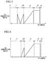
- the difference between the second example and the first example is that, in contrast to the Ge composition ratio being set to be constant in the first SiGe layer 2 in the first example, in the second example, Ge composition ratio x of a first SiGe layer 12 is made to be the intralayer maximum value at the contact surface with Si substrate 1, and Ge composition ratio x is gradually decreased as shown in Fig. 4 .
- Ge composition ratio x is made to be 0.2 at the start of deposition, after which it is gradually decreased until ultimately Ge composition ratio x changes to nearly zero, resulting in an incremental composition layer that is only grown to a predetermined thickness that is thinner than the film thickness at which remarkable generation of dislocation and lattice relaxation actually begins (e.g., 350 nm).
- the Ge composition ratio x of the first SiGe layer 12 by making the Ge composition ratio x of the first SiGe layer 12 the intralayer maximum value at the contact surface with Si substrate 1, strain energy during deposition is concentrated on the side of the interface with Si substrate 1, and during lattice relaxation that occurs at the start of deposition of second SiGe layer 3, greater dislocation is generated at the interface with Si substrate 1 than at the interface with second SiGe layer 3.
- dislocation can be concentrated at a location away from the surface of second SiGe layer 3, thereby making it possible to reduce penetrating dislocation and surface roughness in the same manner as the first example.
- first SiGe layer 22 is made to be in the form of a variable composition layer that is deposited to a predetermined thickness (e.g., 175 nm) by making the Ge composition ratio x at the start of deposition 0.2, and after depositing to a predetermined thickness (e.g., 175 nm) by subsequently gradually decreasing Ge composition ratio x and changing it to nearly zero, the Ge composition ratio x is then again gradually increased, finally reaching a Ge composition ratio x of 0.2.
- a predetermined thickness e.g. 175 nm
- this first SiGe layer 22 is set to be thinner than the film thickness at which remarkable generation of dislocation and lattice relaxation actually begins.
- the difference between the fourth example and the first example is that, in contrast to the Ge composition ratio being set to be constant in the first SiGe layer 2 in the first example, in the fourth example as shown in Fig. 6 , the Ge composition ratio x of a first SiGe layer 32 is gradually increased from nearly zero to ultimately 0.2, and deposited at a predetermined thickness (e.g., 350 nm) that is thinner than the film thickness at which remarkable generation of dislocation and lattice relaxation actually begins.
- a predetermined thickness e.g., 350 nm
- the difference between the fifth example and first example is that, in contrast to the Ge composition ratio being set to be constant in the first SiGe layer 2 in the first example, in the fifth example as shown in Fig. 7 , the Ge composition ratio x of a first SiGe layer 42 is deposited at a predetermined thickness (e.g., 175 nm) while gradually increasing from nearly zero to 0.2, and then subsequently deposited at a predetermined thickness (e.g., 175 nm) while gradually decreasing Ge composition ratio x from 0.2 to nearly zero. Furthermore, the thickness of first SiGe layer 42 is set to be thinner than the film thickness at which remarkable generation of dislocation and lattice relaxation actually begin.
- a predetermined thickness e.g. 175 nm
- both first SiGe layers 32 and 42 are formed at a film thickness that is thinner than the film thickness at which remarkable generation of dislocation and lattice relaxation actually begin, dislocation occurs concentrated at the interfaces on both sides of first SiGe layers 32 and 42 during deposition of second SiGe layer 3, thereby making it possible to reduce penetrating dislocation and surface roughness. Furthermore, in the fourth and fifth examples, since the maximum value of the Ge composition ratio in first SiGe layers 32 and 42 is not on the side of the interface with Si substrate 1, greater improvement effects on penetrating dislocation and surface roughness can be obtained than in the first and second examples.
- the first SiGe layer may be in the form of a multilayer film composed of a plurality of SiGe layers having different Ge composition ratios.
- the aforementioned multilayer film may also contain an Si layer.
- composition was changed at a constant ratio relative to film thickness in the case of having changed the Ge composition ratio in the first SiGe layer in each of the aforementioned examples, a structure may also be employed in which that ratio is not constant.
- the first SiGe layer is only required to be a layer that contains Ge and accumulates strain energy, and other distributions of Ge composition ratios may also be employed.
- an incremental composition layer in which the Ge composition ratio is gradually increased was employed for the entire second SiGe layer in each of the aforementioned examples, it may also be in the form of a layer having a multilayer structure composed of incremental composition layers and uniform composition layers. In addition, it may also be in the form of a multilayer film containing an Si layer.
- composition of an incremental composition region in which the Ge composition ratio is gradually increased towards the surface in the second SiGe layer, was changed at a constant ratio relative to film thickness in each of the aforementioned examples, a structure may also be employed in which that ratio is not constant.
- Ge composition ratio of the that incremental composition region may also be changed in steps.
- the second SiGe layer was arranged directly on the first SiGe layer in each of the aforementioned examples, the second SiGe layer may be arranged on the first SiGe layer with an Si layer in between.
- an additional SiGe layer may be arranged on the strained Si layer of the semiconductor wafer W of each example.
- a semiconductor wafer having an SiGe layer was produced as a MOSFET substrate in each of the aforementioned examples, the substrate may be applied to other applications as well.
- the semiconductor substrate and semiconductor substrate manufacturing method may also be applied to a substrate for a solar cell.
- a solar cell substrate may be produced by depositing an SiGe layer of an incremental composition layer, in which the Ge composition ratio is gradually increased to 100% Ge at the uppermost surface, on an Si substrate of each of the aforementioned examples, followed by depositing GeAs (gallium arsenide) thereon.
- GeAs gallium arsenide
- a semiconductor substrate can be obtained having an SOI (silicon on insulator) structure having strained silicon, high quality and a low level of dislocation.
- a semiconductor substrate employing an SOI structure having strained silicon can be produced by the so-called smart cut method.
- the smart cut method is also referred to as the hydrogen injection delamination method, and is a method for cutting away a thin film by using a phenomenon in which a silicon single crystal lattice is partially severed as a result of injecting hydrogen ions, and particularly protons, into silicon single crystal.
- a semiconductor substrate of the present application having an SOI structure in the form of SiGe/SiO2/Si produced in this manner can be preferably used in the production of an SOI substrate like that described in, for example, US Patent No. 5,906,951 .
- the semiconductor substrates that were produced correspond to the aforementioned first example in that, the Ge composition ratios of first SiGe layer 2 were made to be 0.1, 0.15 or 0.2, and a plurality of substrates were produced while changing film thickness. Furthermore, a substrate of the prior art, namely one not provided with a first SiGe layer, was also produced for the sake of comparison.
- both penetrating dislocation density and surface roughness are decreased when the film thickness of the first SiGe layer is at least less than twice the critical film thickness t c .
- FIG. 24A through 24G show micrographs of the course of deposition by a manufacturing method of the prior art
- Figs. 24D through 24G show the course of deposition by the semiconductor substrate manufacturing method of the present application
- Figs. 24B and 24E are micrographs taken at the same point in time
- Figs. 24C and 24F are micrographs taken at the same point in time later during the course of deposition.
- relaxation has not yet begun.
- Fig. 24C relaxation has not yet begun.
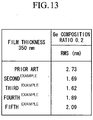
- Fig. 13 results of actually producing semiconductor substrates corresponding to the aforementioned second through fifth examples and measuring surface roughness in the same manner as described above are shown in Fig. 13 .
- the maximum Ge composition ratio of the first SiGe layer is made to be 0.2, and the film thickness is made to be 350 nm in all cases.
- those examples corresponding to the second and third examples demonstrated better results than the other examples.
- the results of measuring penetrating dislocation density and surface roughness versus film thickness of the first SiGe layer for an example corresponding to the second example are shown in Figs. 14 and 15 , respectively.
- penetrating dislocation density and surface roughness are both decreased as compared with the case of the prior art (thickness of first SiGe layer: 0) when the film thickness of the first SiGe layer is at least less than twice the critical film thickness t c .
- Fig. 1 shows the cross-sectional structure of a semiconductor wafer (semiconductor substrate) W useful for the understanding of the present invention.
- first SiGe layer 2 is deposited thinner than the film thickness at which remarkable generation of dislocation and lattice relaxation actually begins, although strain energy increases corresponding to film thickness during deposition of first SiGe layer 2, there is hardly any occurrence of dislocation or lattice relaxation.
- first SiGe layer 2 is a thickness that is thinner than the film thickness at which remarkable generation of dislocation and lattice relaxation actually begins.
- a second SiGe layer 3 is epitaxially grown on first SiGe layer 2.
- the Ge composition ratio y of this second SiGe layer 3 is set to be at least lower than intralayer maximum value of Ge composition ratio x in the first SiGe layer 2 at the contact surface with the first SiGe layer 2.
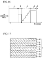
- deposition of the aforementioned second SiGe layer 3 is carried out by repeating a plurality of times at a constant Ge composition ratio a step in which an SiGe incremental composition layer 3a, in which the Ge composition ratio is gradually increased to a predetermined value towards the surface, is epitaxially grown, and a step in which an SiGe constant composition layer 3b is epitaxially grown on incremental composition layer 3a at the final Ge composition ratio of incremental composition layer 3a.
- the Ge composition ratio of the lower surface of the second SiGe layer 3 is set to be equal to or less than the Ge composite layer of the upper second SiGe layer 3 is set to be equal to or less than the Ge composite layer of the upper surface of the first SiGe layer 2.
- the Ge composition ratio of the second SiGe layer 3 is gradually increased from zero.
- a second SiGe layer 3 is formed by repeating the epitaxial growth steps of incremental composition layer 3a and constant composition layer 3b five times. Namely, when one round of epitaxial growth of incremental composition layer 3a and constant composition layer 3b is taken to be one step, the first step consists of growing a first incremental composition layer 3a on Si substrate 1 by gradually increasing the Ge composition ratio from 0 to 0.06, followed by forming a first constant composition layer 3b having a Ge composition ratio is 0.06 thereon.
- the second step consists of growing a second incremental composition layer 3a on the first constant composition layer 3b having a Ge composition ratio of 0.06 by gradually increasing the Ge composition ratio from 0.06 to 0.12, followed by forming a second constant composition layer 3b having a Ge composition ratio of 0.12 thereon.
- the third step consists of growing a third incremental composition layer 3a on the second constant composition layer 3b having a Ge composition ratio of 0.12 by gradually increasing the Ge composition ratio from 0.12 to 0.18, followed by forming a third constant composition layer 3b having a Ge composition ratio of 0.18 thereon.
- the fourth step consists of growing a fourth incremental composition layer 3a on the third constant composition layer 3b having a Ge composition ratio of 0.18 by gradually increasing the Ge composition ratio from 0.18 to 0.24, followed by forming a fourth constant composition layer 3b having a Ge composition ratio of 0.24 thereon.
- the final step consists of growing a fifth incremental composition layer 3a on the fourth constant composition layer 3b having a Ge composition ratio of 0.24 by gradually increasing the Ge composition ratio from 0.24 to 0.3, followed by forming a fifth constant composition layer 3b having a Ge composition ratio of 0.3 thereon.
- the film thicknesses of each incremental composition layer 3a and each constant composition layer 3b are set to be the same.
- the Ge composition ratio of the second SiGe layer 3 is lower than the intralayer maximum value of the Ge composition ratio in the first SiGe layer 2 at the contact surface with the first SiGe layer 2, dislocation occurs concentrated along interfaces 2a and 2b on both sides of first SiGe layer 2, and the generation of dislocation at interfaces 2a and 2b on both sides of first SiGe layer 2 assists in lattice relaxation of second SiGe layer 3, which together with inhibiting generation of dislocation and growth within second SiGe layer 3, inhibits worsening of surface roughness of the surface of second SiGe layer 3.
- a predetermined thickness e.g. 0.75 ⁇ m
- strained Si layer 5 e.g. 20 nm
- the aforementioned deposition by vacuum CVD uses H 2 for the carrier gas and SiH 4 and GeH 4 for the source gases.
- first SiGe layer 2 since the film thickness of first SiGe layer 2 is set to be thinner than the film thickness at which remarkable generation of dislocation and lattice relaxation actually begin, and the composition ratio y of the second SiGe layer 3 is at least made to be lower than the intralayer maximum value of Ge composition ratio x in the first SiGe layer 2 at the contact surface with the first SiGe layer 2, dislocation can be efficiently concentrated in interface 2a between Si substrate 1 and first SiGe layer 2 and interface 2b between first SiGe layer 2 and second SiGe layer 3, thereby making it possible to reduce penetrating dislocation density and surface roughness.
- the film thickness at which generation of dislocation and lattice relaxation actually begin becomes the thinnest at the same Ge composition ratio, thereby offering the advantage of a short time required for deposition since the effects of the present invention are obtained at the thinnest film thickness.
- first SiGe layer 2 by making first SiGe layer 2 to have a thickness that is less than twice the critical film thickness t c that satisfies the aforementioned relational expression, the film thickness of the first SiGe layer 2 can be easily set to be within the film thickness at which remarkable generation of dislocation and lattice relaxation actually begin based on experimental results to be described later.
- the first SiGe layer 2 functions as a layer that removes moisture, oxygen components, carbon components and other impurities on the surface of Si substrate 1, and is effective for inhibiting defects in Si substrate 1 caused by surface contamination.
- MOSFET field effect transistor
- Fig. 3 is a cross-sectional view showing the schematic structure of a field effect transistor useful for the understanding of the present invention.
- an SiO 2 gate oxide film 6 and a gate polysilicon film 7 are sequentially deposited on a strained Si layer 5 on the surface of semiconductor wafer W produced with the aforementioned production process.
- a gate electrode (not shown) is formed by patterning on gate polysilicon film 7 on the portion to serve as a channel region.
- gate oxide film 6 is also patterned to remove the portion other than that beneath the gate electrode. Moreover, an n-type or p-type source region S and a drain region D are formed in a self-matching manner on strained Si layer 5 and relaxation layer 4 by ion injection using the gate electrode as a mask. Subsequently, a source electrode and drain electrode (not shown) are respectively formed on source region S and drain region D to produce an n-type or p-type MOSFET in which strained Si layer 5 serves as the channel region.
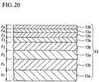
- the difference between the sixth example and the aforementioned embodiment is that, in contrast to the film thicknesses of the incremental composition layer 3a and constant composition layer 3b in the second SiGe layer 3 in the aforementioned embodiment being respectively set to be the same, in the sixth example, as shown in Figs. 19 and 20 , the second SiGe layer 13 is formed by gradually reducing the thicknesses of incremental composition layer 13a and constant composition layer 13b for each repetition of the step in which incremental composition layer 13a and constant composition layer 13b are epitaxially grown.
- the epitaxial growth step of incremental composition layer 3a and constant composition layer 3b is repeated five times in the first example
- the present example differs from this in that the second SiGe layer 13 is formed by repeating the epitaxial growth step of incremental composition layer 13a and constant composition layer 13b four times.
- second incremental composition layer 13a and second constant composition layer 13b are grown to be thinner than first incremental composition layer 13a and first constant composition layer 13b.
- third incremental composition layer 13a and third constant composition layer 13b are similarly grown to be thinner than second incremental composition layer 13a and second constant composition layer 13b, and finally fourth incremental composition layer 13a and fourth constant composition layer 13b are grown to be thinner than third incremental composition layer 13a and third constant composition layer 13b to form second SiGe layer 13.
- first incremental composition layer 13a and first constant composition layer 13b are represented with l 1
- second incremental composition layer 13a and second constant composition layer 13b are represented with l 2
- third incremental composition layer 13a and third constant composition layer 13b are represented with l 3
- fourth incremental composition layer 13a and fourth constant composition layer 13b are represented with l 4
- each of the layers are laminated in the manner of l 1 ⁇ l 2 ⁇ l 3 ⁇ l 4 .
- film thickness is set to be thicker than this critical film thickness, enabling the dislocation required for lattice relaxation to be generated uniformly in each layer.
- each incremental composition layer 13a is set to be the same for each layer.
- dislocation is generated more easily the higher the Ge composition ratio, in the case of repeating deposition at the same thickness as in the aforementioned embodiment, in contrast to more dislocation being generated the higher the layer, by gradually reducing the thickness of incremental composition layer 13a and constant composition layer 13b for each repetition as in the present example, dislocation can be made to be generated uniformly in each layer.
- the seventh example differs from the aforementioned embodiment in that in contrast to the Ge composition ratio being set to be constant in the first SiGe layer 2 in the aforementioned embodiment, in the seventh example, as shown in Figs. 21A through 21D , the Ge composition ratio x of the first SiGe layer is not constant.
- the Ge composition ratio x of the first SiGe layer 12 reaches an intralayer maximum value at the contact surface with Si substrate 1, after which the Ge composition ratio x is gradually decreased.
- the Ge composition ratio x is made to be 0.3 at the start of deposition, after which it is gradually decreased until ultimately Ge composition ratio x changes to nearly zero, resulting in an incremental composition layer that is only grown to a predetermined thickness that is thinner than the film thickness at which remarkable generation of dislocation and lattice relaxation actually begins (e.g., 350 nm).
- the Ge composition ratio x of first SiGe layer 12 by making the Ge composition ratio x of first SiGe layer 12 to be the intralayer maximum value at the contact surface with Si substrate 1, strain energy during deposition is concentrated at the side of the interface with Si substrate 1, there causing greater generation of dislocation at the interface with Si substrate 1 than at the interface with second SiGe layer 3 during lattice relaxation that occurs during deposition of second SiGe layer 3.
- dislocation can be concentrated at a location away from the surface of second SiGe layer 3, thereby making it possible to reduce penetrating dislocation and surface roughness in the same manner as the aforementioned embodiment.
- first SiGe layer 22 is made to be in the form of a variable composition layer that is deposited to a predetermined thickness (e.g., 175 nm) by making the Ge composition ratio x at the start of deposition 0.2, and after depositing to a predetermined thickness (e.g., 175 nm) by subsequently gradually decreasing Ge composition ratio x and changing it to nearly zero, the Ge composition ratio x is then again gradually increased, finally reaching a Ge composition ratio x of 0.2.
- a predetermined thickness e.g. 175 nm
- this first SiGe layer 22 is set to be thinner than the film thickness at which remarkable generation of dislocation and lattice relaxation actually begins.
- the Ge composition ratio x of a first SiGe layer 32 is gradually increased from nearly zero to ultimately 0.2, and deposited at a predetermined thickness (e.g., 175 nm) that is thinner than the film thickness at which remarkable generation of dislocation and lattice relaxation actually begins.
- the Ge composition ratio x of a first SiGe layer 42 is deposited at a predetermined thickness (e.g., 175 nm) while gradually increasing from nearly zero to 0.2, and then subsequently deposited at a predetermined thickness (e.g., 175 nm) while gradually decreasing Ge composition ratio x from 0.2 to nearly zero. Furthermore, the thickness of first SiGe layer 42 is set to be thinner than the film thickness at which remarkable generation of dislocation and lattice relaxation actually begin.
- both first SiGe layers 32 and 42 are formed at a film thickness that is thinner than the film thickness at which remarkable generation of dislocation and lattice relaxation actually begin, dislocation occurs concentrated at the interfaces on both sides of first SiGe layers 32 and 42 during deposition of second SiGe layer 3, thereby making it possible to reduce penetrating dislocation and surface roughness. Furthermore, in this example, since the maximum value of the Ge composition ratio in first SiGe layers 32 and 42 is not on the side of the interface with Si substrate 1, greater improvement effects on penetrating dislocation and surface roughness can be obtained than in the first and second examples.
- the first SiGe layer may be in the form of a multilayer film composed of a plurality of SiGe layers having different Ge composition ratios.
- the aforementioned multilayer film may also contain an Si layer.
- composition was changed at a constant ratio relative to film thickness in the case of having changed the Ge composition ratio in the first SiGe layer in each of the aforementioned examples, a structure may also be employed in which that ratio is not constant.
- the first SiGe layer is only required to be a layer that contains Ge and accumulates strain energy, and other distributions of Ge composition ratios may also be employed.
- composition of an incremental composition layer in which the Ge composition ratio is gradually increased towards the surface in the second SiGe layer was changed at a constant ratio versus film thickness in each of the aforementioned examples, a structure may also be employed in which that ratio is not constant.
- the second SiGe layer was arranged directly on the first SiGe layer in each of the aforementioned examples, the second SiGe layer may be arranged on the first SiGe layer with an Si layer in between.
- an SiGe layer may be additionally deposited on the strained Si layer of a semiconductor wafer of each of the aforementioned examples.
- a solar cell substrate or photo element substrate may be produced by depositing a second SiGe layer and a third SiGe layer so that the uppermost surface is from 65% Ge to 100% Ge or 100% Ge, followed by depositing thereon InGaP (indium-gallium-phosphorous), GaAs (gallium-arsenide) or AlGaAs (aluminum-gallium-arsenide).
- InGaP indium-gallium-phosphorous
- GaAs gallium-arsenide
- AlGaAs aluminum-gallium-arsenide
- the semiconductor substrate that was produced corresponds to the aforementioned embodiment, the Ge composition ratio of the first SiGe layer 2 was made to be 0.2, and an epitaxial growth step for incremental composition layer 3a and constant composition layer 3b of second SiGe layer 3 was repeated five times.
- a plurality of semiconductor substrates were prepared by changing the film thickness of first SiGe layer 2.
- a semiconductor substrate was also prepared for the sake of comparison in which the second SiGe layer was in the form of a single incremental composition layer that did not contain a constant composition layer.
- a semiconductor substrate (STD) was also prepared that did not have a first SiGe layer, and the second SiGe layer was in the form of a single incremental composition layer that did not contain a constant composition layer in order to compare with the prior art.
- the semiconductor substrates provided with even a slight first SiGe layer exhibited lower penetrating dislocation density and surface roughness than the prior art (STD).
- STD penetrating dislocation density and surface roughness
- penetrating dislocation density and surface roughness were poor as compared with the first example, and it can be seen that as a result of employing a layer in the form of incremental steps consisting of an incremental composition layer and constant composition layer for the second SiGe layer, penetrating dislocation density and surface roughness were able to be reduced more effectively.
- the Ge composition ratio of a second SiGe layer is at least made to be lower than the intralayer maximum value of the first SiGe layer at the contact surface with the first SiGe layer or an Si substrate, and the second SiGe layer has an incremental composition layer in which the Ge composition ratio is gradually increased towards the surface at least in a portion thereof, dislocation can be efficiently concentrated at the interface between the Si substrate and first SiGe layer and in the vicinity of the interface between the first SiGe layer and the second SiGe layer, thereby enabling penetrating dislocation density and surface roughness of the surface of the second SiGe layer to be reduced.
- a strained Si layer is epitaxially grown directly on the SiGe layer or with another SiGe layer in between, an Si layer can be deposited on an SiGe layer having satisfactory surface conditions, thereby enabling the formation of a high-quality strained Si layer having few defects and a low level of surface roughness.
- a second SiGe layer is composed in the form of a multilayer laminated layer consisting of an SiGe incremental composition layer, in which the Ge composition ratio is gradually increased towards the surface, and an SiGe constant composition layer, which is arranged on the incremental composition layer at the Ge composition ratio of the upper surface of the incremental composition layer, at an alternating and continuous Ge composition ratio, and the Ge composition ratio of the lower surface of the second SiGe layer is lower than the intralayer maximum value of the Ge composition ratio in the first SiGe layer, together with dislocation being able to be efficiently concentrated at the interface between the Si substrate and first SiGe layer and in the vicinity of the interface between the first SiGe layer and the second SiGe layer, dislocation can be made to propagate in the lateral direction thereby preventing from
Landscapes
- Insulated Gate Type Field-Effect Transistor (AREA)
- Recrystallisation Techniques (AREA)
- Thin Film Transistor (AREA)
Description
- The present invention relates to a semiconductor substrate and field effect transistor used in high-speed MOSFETs and other similar devices, and manufacturing methods of the same.
- High-speed MOSFET, MODFET and HEMT have been proposed in recent years in which an epitaxially grown strained Si layer interposed with an SiGe (silicon-germanium) layer on a Si (silicon) substrate is used for the channel region. In this strained Si-FET, tensile strain occurs in the Si layer due to the SiGe having a larger lattice constant than the Si, and as a result, the band structure of the Si changes, degeneration is removed and carrier mobility increases. Thus, as a result of using this strained Si layer as a channel region, speed can be increased to about 1.3 to 8 times faster than ordinary speeds. In addition, since ordinary Si substrates can be used for the substrates and the CZ (Czochralski method) can be used for the process, high-speed CMOS can be realized with a conventional CMOS process.
- However, although epitaxial growth of a high-quality SiGe layer on an Si substrate is required for epitaxial growth of the aforementioned strained Si layer that is desired to be used as the channel region of an FET, due to the difference in the lattice constants between Si and SiGe, there were problems with crystallinity due to dislocation and so forth. Consequently, the following types of proposals have been made in the prior art.
- Examples of methods that have been proposed include a method that uses a buffer layer in which the composition ratio of Ge in the SiGe is changed at constant, gradual increments, a method that uses a buffer layer in which the composition ratio of Ge (Germanium) is changed in steps, a method that uses a buffer layer in which the Ge composition ratio is changed in the form of a super lattice, and a method that uses a buffer layer in which the Ge composition ratio is changed at a constant increment using an Si off-cut wafer (in, for example,
US Patent No. 5,442,205 ,US Patent No. 5,221,413 ,PCT WO98/00857 6-252046 - However, the aforementioned examples of the prior art still had the problems described below.
- Namely, the SiGe layer deposited using the aforementioned prior art was in a state such that the penetrating dislocation density and surface roughness did not reach the level desirable for use in device and manufacturing processes.
- For example, in the case of using a buffer layer in which the Ge composition ratio is changed incrementally, although penetrating dislocation density can be made to be comparatively low, there is the problem of poor surface roughness. Conversely, in the case of using a buffer layer in which the Ge composition ratio is changed in steps, although surface roughness can be made to be comparatively low, there is the problem of large penetrating dislocation density. In addition, in the case of using an off-cut wafer, although dislocation easily passes through in the lateral direction and not the direction of deposition, it is still not possible to achieve an adequate reduction in dislocation. Surface roughness has also not reached the level required by photolithography processes used for LSI and so forth in recent years.
-
EP 0 889 502 A2WO 01/54167 A -
JP 2000 068283 A US6 388 307 B1 ) describes a bipolar transistor. A bipolar transistor is described which uses a b-doped Si and Ge alloy for a base in which a Ge content in an emitter-base depletion region and in a base-collector depletion region is greater than a Ge content in a base layer. Diffusion of B from the base layer can be suppressed by making the Ge content in the emitter-base depletion region and in a base-collector depletion region on both sides of the base layer greater than the Ge content in the base layer since the diffusion coefficient of B in the SiGe layer is lowered as the Ge content increases. - Document, SEMICONDUCTOR SCIENCE AND TECHNOLOGY, vol. 6, no. 12, pages 1175-1177, December 1991, E Basaran et al, 'Germanium concentration profiling of Si/GexSi1-x heterostructures by anodic dissolution', discloses that an epitaxial layer having a Si/GexSi1-x structure is formed on the Si substrate. A profile of Ge content in the Si/GexSi1-x structure is shown. A Si/GexSi1-x structure A and a Si/GexSi1-x structure B include a Si layer which includes B but does not include Ge in a thickness of 0 to 0.2 µm. A Si layer (including B) and GeSi layer are formed on the Si substrate in this order as the epitaxial layer.
- In consideration of the aforementioned problems, the object of the present invention is to provide a semiconductor substrate, field effect transistor and manufacturing methods thereof that are capable of lowering penetrating dislocation density and surface roughness to practical levels.
- This object is achieved by the features of the independent claims. Advantageous embodiments are described in the dependent claims.
- An example useful for the understanding of the claimed invention employs the following constitution in order to solve the aforementioned problems. Namely, the semiconductor substrate is provided with an Si substrate, a first SiGe layer on the Si substrate, and a second SiGe layer on the first SiGe layer either directly or with an Si layer arranged between the second SiGe layer and the first SiGe layer; wherein, the first SiGe layer has a film thickness that is thinner than twice the critical film thickness, which is the film thickness at which dislocation occurs resulting in lattice relaxation due to increased film thickness, the Ge composition ratio of the second SiGe layer is at least lower than the intralayer maximum value of the Ge composition ratio in the first SiGe layer or in the first SiGe layer at the contact surface with the Si layer, and the second SiGe layer has an incremental composition region in which the Ge composition ratio gradually increases towards the surface at least in a portion thereof.
- In addition, a manufacturing method of a semiconductor substrate is a manufacturing method of a semiconductor substrate in which an SiGe layer is epitaxially grown on an Si substrate, and comprises a first layer formation step in which a first SiGe layer is epitaxially grown on the Si substrate, a second layer formation step in which a second SiGe layer is epitaxially grown on the first SiGe layer either directly or with an epitaxially grown Si layer arranged between the first SiGe layer and the second SiGe layer, in the first layer formation step, the film thickness of the first SiGe layer is set to be thinner than twice the critical film thickness, which is the film thickness at which dislocation occurs resulting in lattice relaxation due to increased film thickness, and in the second layer formation step, the Ge composition ratio of the second SiGe layer is at least lower than the intralayer maximum value of the Ge composition ratio in the first SiGe layer or in the first SiGe layer at the contact surface with the Si layer, and an incremental composition region is formed in which the Ge composition ratio is increased gradually towards the surface in at least a portion thereof.
- In addition, the semiconductor substrate is a semiconductor substrate in which an SiGe layer is formed on an Si substrate, and is fabricated by the aforementioned semiconductor substrate manufacturing method.
- The present example employs the following constitution to solve the aforementioned problems. Namely, the semiconductor substrate is provided with an Si substrate, a first SiGe layer on the Si substrate, and a second SiGe layer on the first SiGe layer either directly or with an Si layer arranged between the second SiGe layer and the first SiGe layer; wherein, the first SiGe layer has a film thickness that is thinner than twice the critical film thickness, which is the film thickness at which dislocation occurs resulting in lattice relaxation due to increased film thickness, the second SiGe layer is composed by laminating multiple layers of an SiGe incremental composition layer, in which the Ge composition ratio gradually increases towards the surface, and an SiGe constant composition layer, which is arranged on an incremental composition layer at the Ge composition ratio of the upper surface of the incremental composition layer, at an alternating and continuous Ge composition ratio, and the Ge composition ratio of the lower surface of the second SiGe layer is lower than the intralayer maximum value of the Ge composition ratio in the first SiGe layer.
- In addition a manufacturing method of a semiconductor substrate is a manufacturing method of a semiconductor substrate in which an SiGe layer is epitaxially grown on an Si substrate, comprising: a first layer formation step in which a first SiGe layer is epitaxially grown on the Si substrate, and a second layer formation step in which a second SiGe layer is epitaxially grown on the first SiGe layer either directly or with an epitaxially grown Si layer arranged between the first SiGe layer and the second SiGe layer, in the first layer formation step, the film thickness of the first SiGe layer is set to be thinner than twice the critical film thickness, which is the film thickness at which dislocation occurs resulting in lattice relaxation due to increased film thickness, and in the second layer formation step, a step in which an SiGe incremental composition layer, in which the Ge composition ratio is gradually increased towards the surface, is epitaxially grown, and a step in which an SiGe constant composition layer is epitaxially grown on the incremental composition layer at the final Ge composition ratio of the incremental composition layer, are repeated a plurality of times at a continuous Ge composition ratio, the second SiGe layer is deposited in which the Ge composition ratio changes in steps at an increment in the direction of deposition, and the Ge composition ratio of the lower surface of the second SiGe layer is lower than the intralayer maximum value of the Ge composition ratio in the first SiGe layer.
- In addition, the semiconductor substrate is a semiconductor substrate in which an SiGe layer is formed on an Si substrate, and is fabricated by the aforementioned semiconductor substrate manufacturing method.
- In this semiconductor substrate and semiconductor substrate manufacturing method, the film thickness of the first SiGe layer is set to be thinner than twice the critical film thickness, which is the film thickness at which dislocation occurs resulting in lattice relaxation due to increased film thickness, the Ge composition ratio of the second SiGe layer is at least lower than the intralayer maximum value of the Ge composition ratio in the first SiGe layer or in the first SiGe layer at the contact surface with the Si layer, and the second SiGe layer has an incremental composition region in which the Ge composition ratio is gradually increased towards the surface in at least a portion thereof. In addition, the Ge composition ratio of the lower surface of the second SiGe layer is lower than the intralayer maximum value of the Ge composition ratio in the first SiGe layer. Consequently, dislocation can be efficiently concentrated in the vicinity of the interface between the Si substrate and the first SiGe layer and the interface of the first SiGe layer and the second SiGe layer, thereby making it possible to reduce penetrating dislocation density and surface roughness on the surface of the second SiGe layer.
- Namely, since a first SiGe layer is deposited to be thinner than twice the critical film thickness, although strain energy corresponding to film thickness during deposition of the first SiGe layer, there is hardly any occurrence of dislocation. Next, when epitaxial growth of the second SiGe layer is begun, since strain energy is already accumulated in the first SiGe layer, the generation of dislocation and growth begin from the interfaces on both sides of the first SiGe layer and from the side of the first SiGe layer within the second SiGe layer at the stage the film thickness of the second SiGe layer is thin, and lattice relaxation of the first SiGe layer and second SiGe layer begins. At this time, since the Ge composition ratio of the second SiGe layer is lower than the intralayer maximum value of the Ge composition ratio in the first SiGe layer or in the first SiGe layer at the contact surface with the aforementioned Si layer, dislocation occurs concentrated along the interfaces on both sides of the first SiGe layer, the generation of dislocation at the interfaces on both sides of the first SiGe layer assists in lattice relaxation of the second SiGe layer, and together with the generation of dislocation and growth within the second SiGe layer being inhibited, worsening of surface roughness of the surface of the second SiGe layer is also inhibited.
- Moreover, the first SiGe layer functions as a layer that removes moisture, oxygen components, carbon components and other impurities on the surface of the Si substrate, and is effective for inhibiting defects in the Si substrate caused by surface contamination.
- Moreover, in the incremental composition region of the second SiGe layer, together with dislocation being generated uniformly, interaction occurs between the dislocation, and the dislocation density within the incremental composition region decreases, and as a result of the growth of dislocation being induced in the lateral direction, penetrating dislocation density in the surface region decreases, thereby also being effective for inhibiting worsening of surface roughness.
- In a conventional incremental composition region in which there is no first SiGe layer, the generation of dislocation begins when the film thickness of the incremental composition region becomes equal to or greater than a predetermined film thickness and exceeds the critical film thickness, and after having once gone through an increase in dislocation density, the aforementioned effects are obtained in the case an incremental composition region is additionally formed. Namely, in the structure of the prior art, the aforementioned effects are only obtained in a portion of the region on the upper side of the incremental composition region.
- On the other hand, in the structure in which there is a first SiGe layer, since strain energy is already accumulated in the first SiGe layer, and the generation of dislocation begins within the second SiGe layer at the stage the film thickness of the second SiGe layer is still thin, the aforementioned effects are obtained throughout the entire incremental composition region within the second SiGe layer, penetrating dislocation density in the surface region of the second SiGe layer decreases, and worsening of surface roughness is inhibited.
- Moreover, the first SiGe layer functions as a layer that removes moisture, oxygen components, carbon components and other impurities on the surface of the Si substrate, and is effective for inhibiting defects in the Si substrate caused by surface contamination.
- Furthermore, when dislocation begins to be generated during deposition of the first SiGe layer, since dislocation begins to grow in multiple directions, it is difficult to inhibit the direction in which dislocation grows, thereby making it difficult to reduce penetrating dislocation and surface roughness. Therefore, it is necessary to set the film thickness of the first SiGe layer to a film thickness that is thinner than film thickness at which remarkable generation of dislocation and lattice relaxation actually begin within a range that does not exceed twice the critical film thickness. At the same time, it is more effective to make the film thickness of the first SiGe layer as close as possible to the film thickness at which remarkable generation of dislocation and lattice relaxation actually begin. The film thickness at which remarkable generation of dislocation and lattice relaxation actually begin varies depending on the temperature conditions of deposition and so forth. Therefore, a film thickness at which the effects are effectively obtained should be selected that is near the film thickness at which remarkable generation of dislocation and lattice relaxation actually begin within a range that does not exceed twice the critical film thickness under each of the deposition conditions.
- In addition, since a second SiGe film is obtained in which a plurality of layers are laminated at an alternating and continuous Ge composition ratio consisting of an SiGe incremental composition layer, in which the Ge composition ratio increases gradually towards the surface, and an SiGe constant composition layer, arranged on an incremental composition layer at the Ge composition ratio of the upper surface of the incremental composition layer, the Ge composition ratio is in the form of incremental steps throughout the second SiGe layer, dislocation occurs easily in the lateral direction at the interface, and together with it being difficult for penetrating dislocation to occur, since there is little change in the composition at the interface, the occurrence of dislocation at the interface is inhibited, intralayer dislocation of the incremental composition layer occurs uniformly, and worsening of surface roughness can be inhibited.
- As a result of conducting research on SiGe deposition technology, it was found that dislocation within crystals exhibits the tendencies described below.
- Namely, when depositing an SiGe layer, dislocation that occurs during deposition has the characteristic of being likely to propagate either in a diagonal direction or lateral direction (direction perpendicular to the direction of deposition: <110> direction) relative to the direction of deposition. In addition, although dislocation tends to propagate easily in the lateral direction at the layer interface, in the case of an interface in which the composition changes rapidly, together with being likely to propagate in the aforementioned diagonal direction, numerous dislocation is thought to occur at high density.
- Thus, when deposition is carried out in which the Ge composition ratio is in the form of simple steps, together with considerable dislocation occurring at high density at the interface sections where there are rapid changes in composition, dislocation easily propagates in a direction diagonal to the direction of deposition, thereby resulting in a high risk of penetrating dislocation. In addition, in the case of deposition in which the Ge composition ratio is simply incremented gradually, there are no sections (such as interfaces) that offer an opportunity for the dislocation propagating in the aforementioned diagonal direction to escape to the lateral direction, and the dislocation is thus thought to end up penetrating to the surface.
- In contrast, in the semiconductor substrate manufacturing method, a step in which an SiGe incremental composition layer, in which the Ge composition ratio is gradually increased towards the surface, is epitaxially grown, and a step in which an SiGe constant composition layer is epitaxially grown on an incremental composition layer at the final Ge composition ratio of the incremental composition layer, are repeated a plurality of times at a continuous Ge composition ratio, and the second SiGe layer is deposited in which the Ge composition ratio changes in steps at increments in the direction of deposition, the incremental composition layers and constant composition layers are formed alternately in a plurality of steps resulting in a layer in which the Ge composition ratio is incremented in steps, thereby enabling the formation of an SiGe layer in which both dislocation density and surface roughness are low.
- Namely, dislocation at an interface propagates easily in the lateral direction making it difficult for penetrating dislocation to occur. In addition, since there is little change in composition at an interface, the occurrence of dislocation at the interface is inhibited, dislocation occurs uniformly within the incremental composition layers, and worsening of surface roughness can be inhibited.
- Moreover, in the incremental composition region of the second SiGe layer, together with dislocation being generated uniformly, interaction occurs between the dislocation, and the dislocation density within the incremental composition region decreases, and as a result of the growth of dislocation being induced in the lateral direction, penetrating dislocation density in the surface region decreases, thereby also being effective for inhibiting worsening of surface roughness.
- In a conventional incremental composition region in which there is no first SiGe layer, the generation of dislocation begins when the film thickness of the incremental composition region becomes equal to or greater than a predetermined film thickness and exceeds the critical film thickness, and after having once gone through an increase in dislocation density, the aforementioned effects are obtained in the case an incremental composition region is additionally formed. Namely, in the structure of the prior art, the aforementioned effects are only obtained in a portion of the region on the upper side of the incremental composition region.
- On the other hand, in the present structure in which there is a first SiGe layer, since strain energy is already accumulated in the first SiGe layer, and the generation of dislocation begins within the second SiGe layer at the stage the film thickness of the second SiGe layer is still thin, the aforementioned effects are obtained throughout the entire incremental composition region within the second SiGe layer, penetrating dislocation density in the surface region of the second SiGe layer decreases, and worsening of surface roughness is inhibited.
- In addition, in the semiconductor substrate, technology is employed in which the Ge composition ratio of the first SiGe layer is constant, and is of a thickness that is thinner than the film thickness at which remarkable generation of dislocation and lattice relaxation actually begin.
- In addition, in the first layer formation step, technology is employed in which the Ge composition ratio of the first SiGe layer is constant, and the first SiGe layer is of a thickness that is thinner than the film thickness at which remarkable generation of dislocation and lattice relaxation actually begin.
- In this semiconductor substrate and semiconductor substrate manufacturing method, since the Ge composition ratio of the first SiGe layer is constant, there are the advantages of the film thickness at which remarkable generation of dislocation and lattice relaxation actually begin at the same Ge composition ratio being the thinnest, the effects being obtained at the thinnest film thickness, and the amount of time required for deposition being short. In addition, in this semiconductor substrate and semiconductor substrate manufacturing method, by making the first SiGe layer of a thickness that is less than twice the critical film thickness tc which satisfies the aforementioned relational expression (referring to the film thickness at which dislocation calculated from the Ge composition ratio and lattice constant only occurs resulting in lattice relaxation regardless of the deposition temperature), the film thickness of the first SiGe layer can easily be set to within a film thickness at which remarkable generation of dislocation and lattice relaxation actually begin.
- Namely, since the film thickness at which remarkable generation of dislocation and lattice relaxation actually begins changes according to the deposition temperature, if the film thickness is made to be less than twice the ideal critical film thickness tc theoretically determined from only the Ge composition ratio x and the lattice constant, it becomes thinner than the film thickness at which remarkable generation of dislocation and lattice relaxation actually begin, thereby allowing the effects to be obtained. Furthermore, since the aforementioned critical film thickness is premised on being deposited in an equilibrium state, although it is determined with only the Ge composition ratio and lattice constant regardless of the deposition temperature, the film thickness at which remarkable generation of dislocation and lattice relaxation actually begin includes not only an equilibrium state, but also deposition in non-equilibrium state such as low-temperature growth, and is determined corresponding to deposition temperature.
- In addition, in the semiconductor substrate of an example not forming part of the claimed invention, the Ge composition ratio x of the first SiGe layer is preferably from 0.05 to 0.3.
- In addition, in the semiconductor substrate manufacturing method of an example not forming part of the claimed invention the Ge composition ratio x of the first SiGe layer is preferably from 0.05 to 0.3.
- In addition, in the semiconductor substrate manufacturing method, a semiconductor substrate is preferably produced in which a strained Si layer is formed on an Si substrate with an SiGe layer in between the strained Si layer and Si substrate, and the strained Si layer is preferably grown on a second SiGe layer of the semiconductor substrate either directly or with another SiGe layer in between.
- The semiconductor substrate is characterized by being a semiconductor substrate in which an SiGe layer is formed on an Si substrate, and is produced according to the aforementioned semiconductor substrate manufacturing method. Namely, since this semiconductor substrate is produced according to the aforementioned semiconductor substrate manufacturing method, there is little penetrating dislocation of the surface and it has satisfactory surface roughness.
- In this semiconductor substrate and semiconductor substrate manufacturing method, which does not form part of the claimed invention, since the Ge composition ratio of the first SiGe layer is from 0.05 to 0.3, the film thickness at which remarkable generation of dislocation and lattice relaxation actually begins is neither too thin or too thick, and the effects of the present invention are effectively obtained with a first SiGe layer of a suitable thickness.
- Namely, in the case the Ge composition ratio x of the first SiGe layer is less than 0.05, since the film thickness at which remarkable generation of dislocation and lattice relaxation actually begins becomes excessively thick, the time required to deposit the first SiGe layer becomes long, and the surface roughness of the first SiGe layer worsens.
- On the other hand, in the case the Ge composition ratio x of the first SiGe layer is greater than 0.3, since generation of dislocation and lattice relaxation actually end up beginning at an extremely thin film thickness, it is difficult to form the first SiGe layer with satisfactory controllability.
- In addition, if the aforementioned Ge composition ratio x of the first SiGe layer is from 0.05 to 0.3, the film thickness at which remarkable generation of dislocation and lattice relaxation actually begin becomes a suitable thickness, dislocation occurs concentrated along the interfaces on both sides of the first SiGe layer, and the effect in which the generation of dislocation at the interfaces on both sides of the first SiGe layer assists in lattice relaxation of the second SiGe layer is effectively obtained.
- In addition, in the semiconductor substrate, a structure is employed in which the second SiGe layer is arranged directly on the first SiGe layer, and the entire layer is in the form of an incremental composition layer in which the Ge composition ratio has been gradually increased towards the surface.
- In addition, in the semiconductor substrate manufacturing method, a method is employed in which the second SiGe layer is arranged directly on the first SiGe layer, and the entire layer is in the form of an incremental composition layer in which the Ge composition ratio has been gradually increased towards the surface.
- In addition, the semiconductor substrate is characterized by being a semiconductor substrate in which an SiGe layer is formed on an Si substrate, and is produced according to the aforementioned semiconductor substrate manufacturing method.
- The semiconductor substrate is characterized by epitaxial growth of a strained Si layer on the second SiGe layer either directly or with another SiGe layer in between.
- The semiconductor substrate manufacturing method is characterized by having a step in which a strained Si layer is epitaxially grown on the second SiGe layer either directly or with another SiGe layer in between.
- In addition, the semiconductor substrate is characterized by being a semiconductor substrate in which a strained Si layer is formed on an Si substrate with an SiGe layer in between, and is produced according to the aforementioned semiconductor substrate manufacturing method.
- In this semiconductor substrate and semiconductor substrate manufacturing method, since the second SiGe layer is directly arranged on the first SiGe layer, and the entire layer is in the form of an incremental composition layer in which the Ge composition ratio is gradually increased towards the surface, layers required for obtaining the effects are not provided wastefully and the effects are obtained with the thinnest film thickness, thereby offering the advantage of a short time required for deposition.
- In this semiconductor substrate and semiconductor substrate manufacturing method, since a strained Si layer is epitaxially grown on the second SiGe layer either directly or with another SiGe layer in between, there are few defects, a high-quality strained Si layer is obtained having little surface roughness, and a semiconductor substrate can be obtained that is suitable for use in, for example, an integrated circuit using a MOSFET and so forth in which the strained Si layer is used as a channel region.
- The semiconductor substrate is characterized by epitaxial growth of a strained Si layer on the aforementioned SiGe layer either directly or with another SiGe layer in between.
- In addition, the semiconductor substrate manufacturing method is characterized by epitaxially growing a strained Si layer on the aforementioned SiGe layer either directly or with another SiGe layer in between.
- In addition, the semiconductor substrate is characterized by being a semiconductor substrate in which a strained Si layer is formed on an Si substrate with an SiGe layer in between, and is produced according to the aforementioned semiconductor substrate manufacturing method in which a strained Si layer is grown.
- In this semiconductor substrate and semiconductor substrate manufacturing method, since a strained Si layer is epitaxially grown on the SiGe layer either directly or with another SiGe layer in between, there are few defects, a high-quality strained Si layer is obtained having little surface roughness, and the semiconductor substrate and its manufacturing method are suitable for use in, for example, an integrated circuit using a MOSFET and so forth in which the strained Si layer is used as a channel region.
- The field effect transistor is characterized by being a field effect transistor having a channel region in a strained Si layer on an SiGe layer, and having the channel region in the strained Si layer of the semiconductor substrate.
- In addition, the field effect transistor manufacturing method is characterized by being a field effect transistor manufacturing method in which a channel region is formed in a strained Si layer epitaxially grown on an SiGe layer, and forms the channel region in the strained Si layer of a semiconductor substrate produced according to the aforementioned semiconductor substrate manufacturing method.
- In addition, the field effect transistor is characterized by being a field effect transistor in which a channel region is formed in a strained Si layer epitaxially grown on an SiGe layer, and being produced according to the field effect transistor manufacturing method.
- In addition, the field effect transistor manufacturing method is characterized by being a field effect transistor manufacturing method in which a channel region is formed in a strained Si layer epitaxially grown on an SiGe layer, and forms the channel region in the strained Si layer of a semiconductor substrate produced according to the semiconductor substrate manufacturing method in which the semiconductor substrate has a strained Si layer.
- In addition, the field effect transistor is characterized by being a field effect transistor in which a channel region is formed in a strained Si layer epitaxially grown on an SiGe layer, and is produced according to the field effect transistor manufacturing method.
- In this field effect transistor and field effect transistor manufacturing method, since the channel region is formed in the strained Si layer of the semiconductor substrate or a semiconductor substrate produced according to the semiconductor substrate manufacturing method, a high-performance field effect transistor can be obtained at high yield due to a high-quality strained Si layer.
-
-
Fig. 1 is a cross-sectional view showing a semiconductor substrate useful for the understanding of the present invention. -
Fig. 2 is a graph showing the Ge composition ratio versus the film thickness of a semiconductor substrate in a first example not forming part of the claimed invention. -
Fig. 3 is a schematic cross-sectional view showing a MOSFET useful for the understanding of the present invention. -
Fig. 4 is a graph showing the Ge composition ratio versus film thickness of a semiconductor substrate in a second example not forming part of the claimed invention. -
Fig. 5 is a graph showing the Ge composition ratio versus film thickness of a semiconductor substrate in a third example not forming part of the claimed invention. -
Fig. 6 is a graph showing the Ge composition ratio versus film thickness of a semiconductor substrate in a fourth example not forming part of the claimed invention. -
Fig. 7 is a graph showing the Ge composition ratio versus film thickness of a semiconductor substrate in a fifth example not forming part of the claimed invention. -
Fig. 8 is a graph showing the results of SIMS analysis of the distribution of Ge composition ratio versus film thickness for semiconductor substrates in an example corresponding to the first example and not forming part of the claimed invention in which the film thickness of a first SiGe layer is made to be 300 nm. -
Fig. 9 is a graph showing the penetrating dislocation density versus film thickness of a first SiGe layer in an example corresponding to the first example and not forming part of the claimed invention. -
Fig. 10 is a graph showing the surface roughness versus film thickness of a first SiGe layer in an example corresponding to the first example and not forming part of the claimed invention. -
Fig. 11 is an electron micrograph of the surface in an example of the prior art relating to the present invention. -
Fig. 12 is an electron micrograph of the surface in a first example not forming part of the claimed invention. -
Fig. 13 is a table showing the respective surface roughness in examples corresponding to the second through fifth examples and not forming part of the claimed invention. -
Fig. 14 is a graph showing the results of measuring penetrating dislocation density versus film thickness of a first SiGe layer in an example corresponding to the second example and being useful for the understanding of the present invention. -
Fig. 15 is a graph showing the results of measuring the surface roughness versus film thickness of first SiGe layer in an example corresponding to the second example and being useful for the understanding of the invention. -
Fig. 16 is a graph showing the Ge composition ratio versus film thickness of a semiconductor substrate in an embodiment as claimed in the present invention. -
Fig. 17 is a cross-sectional view showing a second SiGe layer in an embodiment as claimed in the present invention. -
Fig. 18 is a graph showing the Ge composition ratio versus film thickness of a second SiGe layer in an embodiment as claimed in the present invention. -
Fig. 19 is a graph showing the Ge composition ratio versus film thickness of a second SiGe layer in a second example not forming part of the claimed invention. -
Fig. 20 is a cross-sectional view showing a second SiGe layer in a second example not forming part of the claimed invention. -
Figs. 21A through 21D are graphs showing the Ge composition ratio versus film thickness of a first SiGe layer in respective examples of the third example and not forming part of the claimed invention. -
Fig. 22 is a graph showing the results of measuring penetrating dislocation density in the case of changing the film thickness of a first SiGe layer in an embodiment as claimed in the present invention. -
Fig. 23 is a graph showing the results of measuring surface roughness in the case of changing the film thickness of a first SiGe layer in an embodiment of the present invention. -
Figs. 24A to 24G are photographs of the result of observing a deposition process with a transmission electron microscope (TEM). - The following provides an explanation of a first example not forming part of the claimed invention with reference to
Figs. 1 through 3 . -
Fig. 1 shows the cross-sectional structure of a semiconductor wafer (semiconductor substrate) W. The following provides an explanation of the structure of this semiconductor wafer along with its manufacturing process. First, as shown inFigs. 1 and 2 , afirst SiGe layer 2, in which the Ge composition ratio x is constant (e.g., x = 0.15) and which has a thickness that is thinner than the film thickness at which remarkable generation of dislocation and lattice generation actually begins (e.g., 300 nm), is epitaxially grown by, for example, a vacuum CVD method on a p-type or n-type Si substrate 1 produced by drawing and growing using the CZ method and so forth. - At this time, since the
first SiGe layer 2 is deposited thinner than the film thickness at which remarkable generation of dislocation and lattice relaxation actually begins, although strain energy increases corresponding to film thickness during deposition offirst SiGe layer 2, there is hardly any occurrence of dislocation or lattice relaxation. - Furthermore, the thickness of
first SiGe layer 2 is a thickness that is thinner than the film thickness at which remarkable generation of dislocation and lattice relaxation actually begin. - Next, a
second SiGe layer 3 is epitaxially grown onfirst SiGe layer 2. The Ge composition ratio y of thissecond SiGe layer 3 is set to be at least lower than intralayer maximum value of Ge composition ratio x in thefirst SiGe layer 2 at the contact surface with thefirst SiGe layer 2. In addition, thesecond SiGe layer 3 is an incremental composition layer in which its Ge composition ratio y gradually increases towards the surface (e.g., a layer in which Ge composition ratio y increases from 0 to 0.3) (incremental composition region), and is deposited to a thickness of, for example, 1.1 µm. - When epitaxial growth of
second SiGe layer 3 is started, since strain energy is already accumulated infirst SiGe layer 2, generation of dislocation and growth begin from the interfaces on both sides offirst SiGe layer 2 and from the side offirst SiGe layer 2 insecond SiGe layer 3, and lattice relaxation offirst SiGe layer 2 andsecond SiGe layer 3 begins at the stage the film thickness ofsecond SiGe layer 3 is thin. At this time, since the Ge composition ratio of thesecond SiGe layer 3 is lower than the intralayer maximum value of the Ge composition ratio in thefirst SiGe layer 2 at the contact surface with thefirst SiGe layer 2, dislocation occurs concentrated alonginterfaces 2a and 2b on both sides offirst SiGe layer 2, and the generation of dislocation ininterfaces 2a and 2b on both sides offirst SiGe layer 2 assists the lattice relaxation ofsecond SiGe layer 3, which together with inhibiting generation of dislocation and growth withinsecond SiGe layer 3, also inhibits worsening of surface roughness of the surface ofsecond SiGe layer 3. - Moreover, the semiconductor wafer W is produced by epitaxially growing an
SiGe relaxation layer 4 having a constant composition ratio, in which Ge composition ratio z is the same as the final Ge composition ratio of the second SiGe layer 3 (e.g., z = 0.3), to a predetermined thickness (e.g., 0.75 µm), epitaxially growing single crystal Si on theSiGe relaxation layer 4, and then formingstrained Si layer 5 to a predetermined thickness (e.g., 20 nm). - Furthermore, the aforementioned deposition by vacuum CVD uses H2 for the carrier gas and SiH4 and GeH4 for the source gases.
- In this type of semiconductor wafer W, since the film thickness of the
first SiGe layer 2 is set to be thinner than the film thickness at which remarkable generation of dislocation and lattice relaxation actually begin, and the Ge composition ratio y of thesecond SiGe layer 3 is made to at least be lower than the intralayer maximum value of Ge composition ratio x in thefirst SiGe layer 2 at the contact surface with thefirst SiGe layer 2, dislocation can be efficiently concentrated in interface 2a betweenSi substrate 1 andfirst SiGe layer 2 andinterface 2b betweenfirst SiGe layer 2 andsecond SiGe layer 3, thereby making it possible to reduce penetrating dislocation density and surface roughness. - In addition, since the Ge composition ratio of the
first SiGe layer 2 is constant, the film thickness at which remarkable generation of dislocation and lattice relaxation actually begin becomes the thinnest at the same Ge composition ratio, thereby offering the advantage of a short time required for deposition since the effects are obtained at the thinnest film thickness. - In addition, as a result of making
first SiGe layer 2 have a thickness that is less than twice the critical thickness tc that satisfies the aforementioned relational expression, the film thickness of thefirst SiGe layer 2 can be easily set to be within the film thickness at which remarkable generation of dislocation and lattice relaxation actually begin based on experimental results to be described later. - In addition, as a result of the
second SiGe layer 3 being in the form of an incremental composition layer (incremental composition region) in which the Ge composition ratio is gradually increased, dislocation is generated uniformly, interaction between dislocations occurs, and together with reducing dislocation density within thesecond SiGe layer 3, since the growth of dislocation is induced in the lateral direction, penetrating dislocation density in the surface region decreases, thereby demonstrating the effect of inhibiting worsening of surface roughness. - In addition, in the present example, since strain energy is already accumulated in the
first SiGe layer 2 prior to deposition of thesecond SiGe layer 3, the aforementioned effects are obtained throughout the entire incremental composition region withinsecond SiGe layer 3 since generation of dislocation begins within thesecond SiGe layer 3, penetrating dislocation density in the surface region ofsecond SiGe layer 3 decreases and worsening of surface roughness is inhibited. - Moreover,
first SiGe layer 2 functions as a layer that removes moisture, oxygen components, carbon components and other impurities on the surface ofSi substrate 1, and has the effect of inhibiting defects caused by surface contamination ofSi substrate 1. - Next, an explanation is provided of a field effect transistor (MOSFET) that uses the aforementioned semiconductor wafer W along with its manufacturing process with reference to
Fig. 3 . -
Fig. 3 shows the schematic structure of a field effect transistor. In producing this field effect transistor, an SiO2gate oxide film 6 and a gate polysilicon film 7 are sequentially deposited on astrained Si layer 5 on the surface of semiconductor wafer W produced with the aforementioned manufacturing process. A gate electrode (not shown) is formed by patterning on gate polysilicon film 7 on the portion to serve as a channel region. - Next,
gate oxide film 6 is also patterned to remove the portion other than that beneath the gate electrode. Moreover, an n-type or p-type source region S and a drain region D are formed in a self-matching manner onstrained Si layer 5 andrelaxation layer 4 by ion injection using the gate electrode as a mask. Subsequently, a source electrode and drain electrode (not shown) are respectively formed on source region S and drain region D to produce an n-type or p-type MOSFET in which strainedSi layer 5 serves as the channel region. - In a MOSFET produced in this manner, since a channel region is formed on
strained Si layer 5 on a semiconductor wafer W produced with the aforementioned manufacturing method, a MOSFET offering even better characteristics can be obtained at high yield on a high-qualitystrained Si layer 5. - Next, an explanation is provided of a second example not forming part of the claimed invention with reference to
Fig. 4 . - The difference between the second example and the first example is that, in contrast to the Ge composition ratio being set to be constant in the
first SiGe layer 2 in the first example, in the second example, Ge composition ratio x of afirst SiGe layer 12 is made to be the intralayer maximum value at the contact surface withSi substrate 1, and Ge composition ratio x is gradually decreased as shown inFig. 4 . - Namely, in the present example, in the formation step of
first SiGe layer 12, Ge composition ratio x is made to be 0.2 at the start of deposition, after which it is gradually decreased until ultimately Ge composition ratio x changes to nearly zero, resulting in an incremental composition layer that is only grown to a predetermined thickness that is thinner than the film thickness at which remarkable generation of dislocation and lattice relaxation actually begins (e.g., 350 nm). - In the present example, by making the Ge composition ratio x of the
first SiGe layer 12 the intralayer maximum value at the contact surface withSi substrate 1, strain energy during deposition is concentrated on the side of the interface withSi substrate 1, and during lattice relaxation that occurs at the start of deposition ofsecond SiGe layer 3, greater dislocation is generated at the interface withSi substrate 1 than at the interface withsecond SiGe layer 3. As a result, dislocation can be concentrated at a location away from the surface ofsecond SiGe layer 3, thereby making it possible to reduce penetrating dislocation and surface roughness in the same manner as the first example. - Next, an explanation is provided of a third example not forming part of the claimed invention with reference to
Fig. 5 . - The difference between the third example and second example is that, in contrast to the
second SiGe layer 12 of the second example being an incremental composition layer in which the Ge composition ratio is gradually increased, in the third example, in the formation step offirst SiGe layer 22 as shown inFig. 5 ,first SiGe layer 22 is made to be in the form of a variable composition layer that is deposited to a predetermined thickness (e.g., 175 nm) by making the Ge composition ratio x at the start of deposition 0.2, and after depositing to a predetermined thickness (e.g., 175 nm) by subsequently gradually decreasing Ge composition ratio x and changing it to nearly zero, the Ge composition ratio x is then again gradually increased, finally reaching a Ge composition ratio x of 0.2. - Furthermore, the thickness of this
first SiGe layer 22 is set to be thinner than the film thickness at which remarkable generation of dislocation and lattice relaxation actually begins. - In this third example as well, since the Ge composition ratio x of the
first SiGe layer 22 becomes the intralayer maximum value at the contact surface withSi substrate 1 andsecond SiGe layer 3, similar to the first example, a large amount of dislocation occurs at the interface withSi substrate 1 andsecond SiGe layer 3. - Next, an explanation is provided of fourth and fifth examples not forming part of the claimed invention with reference to
Figs. 6 and7 . - The difference between the fourth example and the first example is that, in contrast to the Ge composition ratio being set to be constant in the
first SiGe layer 2 in the first example, in the fourth example as shown inFig. 6 , the Ge composition ratio x of afirst SiGe layer 32 is gradually increased from nearly zero to ultimately 0.2, and deposited at a predetermined thickness (e.g., 350 nm) that is thinner than the film thickness at which remarkable generation of dislocation and lattice relaxation actually begins. - In addition, the difference between the fifth example and first example is that, in contrast to the Ge composition ratio being set to be constant in the
first SiGe layer 2 in the first example, in the fifth example as shown inFig. 7 , the Ge composition ratio x of afirst SiGe layer 42 is deposited at a predetermined thickness (e.g., 175 nm) while gradually increasing from nearly zero to 0.2, and then subsequently deposited at a predetermined thickness (e.g., 175 nm) while gradually decreasing Ge composition ratio x from 0.2 to nearly zero. Furthermore, the thickness offirst SiGe layer 42 is set to be thinner than the film thickness at which remarkable generation of dislocation and lattice relaxation actually begin. - In these fourth and fifth examples, since both first SiGe layers 32 and 42 are formed at a film thickness that is thinner than the film thickness at which remarkable generation of dislocation and lattice relaxation actually begin, dislocation occurs concentrated at the interfaces on both sides of first SiGe layers 32 and 42 during deposition of
second SiGe layer 3, thereby making it possible to reduce penetrating dislocation and surface roughness. Furthermore, in the fourth and fifth examples, since the maximum value of the Ge composition ratio in first SiGe layers 32 and 42 is not on the side of the interface withSi substrate 1, greater improvement effects on penetrating dislocation and surface roughness can be obtained than in the first and second examples. - For example, although five types of distributions were used in each of the aforementioned examples for the distribution of the Ge composition ratio versus film thickness in the first SiGe layer, other types of distribution may also be employed. For example, the first SiGe layer may be in the form of a multilayer film composed of a plurality of SiGe layers having different Ge composition ratios. In addition, the aforementioned multilayer film may also contain an Si layer.
- In addition, although the composition was changed at a constant ratio relative to film thickness in the case of having changed the Ge composition ratio in the first SiGe layer in each of the aforementioned examples, a structure may also be employed in which that ratio is not constant.
- Moreover, the first SiGe layer is only required to be a layer that contains Ge and accumulates strain energy, and other distributions of Ge composition ratios may also be employed.
- In addition, although an incremental composition layer in which the Ge composition ratio is gradually increased was employed for the entire second SiGe layer in each of the aforementioned examples, it may also be in the form of a layer having a multilayer structure composed of incremental composition layers and uniform composition layers. In addition, it may also be in the form of a multilayer film containing an Si layer.
- In addition, although the composition of an incremental composition region, in which the Ge composition ratio is gradually increased towards the surface in the second SiGe layer, was changed at a constant ratio relative to film thickness in each of the aforementioned examples, a structure may also be employed in which that ratio is not constant. In addition, the Ge composition ratio of the that incremental composition region may also be changed in steps.
- In addition, although the second SiGe layer was arranged directly on the first SiGe layer in each of the aforementioned examples, the second SiGe layer may be arranged on the first SiGe layer with an Si layer in between.
- In addition, an additional SiGe layer may be arranged on the strained Si layer of the semiconductor wafer W of each example.
- In addition, although a semiconductor wafer having an SiGe layer was produced as a MOSFET substrate in each of the aforementioned examples, the substrate may be applied to other applications as well. For example, the semiconductor substrate and semiconductor substrate manufacturing method may also be applied to a substrate for a solar cell. Namely, a solar cell substrate may be produced by depositing an SiGe layer of an incremental composition layer, in which the Ge composition ratio is gradually increased to 100% Ge at the uppermost surface, on an Si substrate of each of the aforementioned examples, followed by depositing GeAs (gallium arsenide) thereon. In this case, a solar cell substrate is obtained having superior characteristics and low dislocation density.
- In addition, according to the semiconductor substrate manufacturing method, a semiconductor substrate can be obtained having an SOI (silicon on insulator) structure having strained silicon, high quality and a low level of dislocation. A semiconductor substrate employing an SOI structure having strained silicon can be produced by the so-called smart cut method. The smart cut method is also referred to as the hydrogen injection delamination method, and is a method for cutting away a thin film by using a phenomenon in which a silicon single crystal lattice is partially severed as a result of injecting hydrogen ions, and particularly protons, into silicon single crystal. A semiconductor substrate of the present application having an SOI structure in the form of SiGe/SiO2/Si produced in this manner can be preferably used in the production of an SOI substrate like that described in, for example,
US Patent No. 5,906,951 . - Next, an explanation is provided of the analysis results of a semiconductor substrate as determined by SIMS (Secondary Ion Mass Spectrometry) at the time of actual production, and the results of observing penetrating dislocation density, surface roughness and surface electron micrographs.
- The semiconductor substrates that were produced correspond to the aforementioned first example in that, the Ge composition ratios of
first SiGe layer 2 were made to be 0.1, 0.15 or 0.2, and a plurality of substrates were produced while changing film thickness. Furthermore, a substrate of the prior art, namely one not provided with a first SiGe layer, was also produced for the sake of comparison. - Among these semiconductor substrates, the results of analyzing the distribution of Ge composition ratio versus film thickness by SIMS for substrates in which the film thickness of the
first SiGe layer 2 is made to be 300 nm are shown inFig. 8 . - The results of measuring the penetrating dislocation density and surface roughness of these semiconductor substrates are shown in
Figs. 9 and10 , respectively. Furthermore, penetrating dislocation density is represented with etch pit density, while surface roughness is represented with RMS (root mean square). - As can be understood from these graphs, in comparison with the case of the prior art (thickness of first SiGe layer: 0), both penetrating dislocation density and surface roughness are decreased when the film thickness of the first SiGe layer is at least less than twice the critical film thickness tc.
- In addition, surface electron micrographs in the case of the prior art (thickness of first SiGe layer: 0) and the case of the aforementioned examples in which the Ge composition ratio of the first SiGe layer is 0.2 and the thickness of the first SiGe layer is 180 nm are shown in
Figs. 11 and12 , respectively. - As can be understood from these micrographs, there are very few dark points corresponding to etching pits in the case of the present example as compared with the case of the prior art.
- Furthermore, electron micrographs of the results of observing the course of deposition with a transmission electron microscope (TEM) are shown for the present examples in
Figs. 24A through 24G. Figs. 24A through 24C show micrographs of the course of deposition by a manufacturing method of the prior art, whileFigs. 24D through 24G show the course of deposition by the semiconductor substrate manufacturing method of the present application.Figs. 24B and 24E are micrographs taken at the same point in time, whileFigs. 24C and 24F are micrographs taken at the same point in time later during the course of deposition. InFig. 24C , relaxation has not yet begun. In contrast, according toFig. 24F , considerable dislocation has occurred at the interface between the first SiGe layer and the Si substrate and at the interface between the first SiGe layer and the second SiGe layer, and there can be confirmed to be very little dislocation on the surface side of the second SiGe layer, and relaxation can be confirmed to already be proceeding at both interfaces of the first SiGe layer. - In addition, the results of actually producing semiconductor substrates corresponding to the aforementioned second through fifth examples and measuring surface roughness in the same manner as described above are shown in
Fig. 13 . Furthermore, the maximum Ge composition ratio of the first SiGe layer is made to be 0.2, and the film thickness is made to be 350 nm in all cases. As can be understood fromFig. 13 , in these embodiments, those examples corresponding to the second and third examples demonstrated better results than the other examples. The results of measuring penetrating dislocation density and surface roughness versus film thickness of the first SiGe layer for an example corresponding to the second example are shown inFigs. 14 and15 , respectively. Similar to the case of the first example, penetrating dislocation density and surface roughness are both decreased as compared with the case of the prior art (thickness of first SiGe layer: 0) when the film thickness of the first SiGe layer is at least less than twice the critical film thickness tc. - The following provides an explanation of an embodiment as claimed in the present invention with reference to
Figs. 1 ,3 ,16, 17 and18 . -
Fig. 1 shows the cross-sectional structure of a semiconductor wafer (semiconductor substrate) W useful for the understanding of the present invention. The following provides an explanation of the structure of this semiconductor wafer along with its production process. First, as shown inFig. 16 , afirst SiGe layer 2, in which the Ge composition ratio x is constant (e.g., x = 0.15) and which has a thickness that is thinner than the film thickness at which remarkable generation of dislocation and lattice generation actually begins (e.g., 300 nm), is epitaxially grown by, for example, a vacuum CVD method on a p-type or n-type Si substrate 1 produced by drawing and growing using the CZ method and so forth. - At this time, since the
first SiGe layer 2 is deposited thinner than the film thickness at which remarkable generation of dislocation and lattice relaxation actually begins, although strain energy increases corresponding to film thickness during deposition offirst SiGe layer 2, there is hardly any occurrence of dislocation or lattice relaxation. - Furthermore, the thickness of
first SiGe layer 2 is a thickness that is thinner than the film thickness at which remarkable generation of dislocation and lattice relaxation actually begins. - Next, a
second SiGe layer 3 is epitaxially grown onfirst SiGe layer 2. The Ge composition ratio y of thissecond SiGe layer 3 is set to be at least lower than intralayer maximum value of Ge composition ratio x in thefirst SiGe layer 2 at the contact surface with thefirst SiGe layer 2. In addition, thesecond SiGe layer 3 is a stepwise increment layer of Si1-xGex in which the Ge composition ratio x changes in steps from 0 to y (where y = 0.3, for example) at an increment moving towards the direction of deposition. - Next, a
relaxation layer 4 of Si1-yGey, in which the Ge composition ratio is constant, is epitaxially grown onsecond SiGe layer 3. Moreover, by forming astrained Si layer 5 by epitaxially growing Si on Si1-yGey relaxation layer 4 at Ge composition ratio z (z = y in the present embodiment), a semiconductor wafer W is produced that is provided with a strained Si layer of the present embodiment. Furthermore, in the present embodiment, the thickness of thesecond SiGe layer 3 is, for example, 1.5 µm, that of the relaxation layer is 0.7-0.8 µm, and that ofstrained Si layer 5 is 15-22 nm. - As shown in
Figs. 16 through 18 , deposition of the aforementionedsecond SiGe layer 3 is carried out by repeating a plurality of times at a constant Ge composition ratio a step in which an SiGeincremental composition layer 3a, in which the Ge composition ratio is gradually increased to a predetermined value towards the surface, is epitaxially grown, and a step in which an SiGeconstant composition layer 3b is epitaxially grown onincremental composition layer 3a at the final Ge composition ratio ofincremental composition layer 3a. In addition, the Ge composition ratio of the lower surface of thesecond SiGe layer 3 is set to be equal to or less than the Ge composite layer of the uppersecond SiGe layer 3 is set to be equal to or less than the Ge composite layer of the upper surface of thefirst SiGe layer 2. Furthermore, in the present embodiment, the Ge composition ratio of thesecond SiGe layer 3 is gradually increased from zero. - For example, in the present embodiment, a
second SiGe layer 3 is formed by repeating the epitaxial growth steps ofincremental composition layer 3a andconstant composition layer 3b five times. Namely, when one round of epitaxial growth ofincremental composition layer 3a andconstant composition layer 3b is taken to be one step, the first step consists of growing a firstincremental composition layer 3a onSi substrate 1 by gradually increasing the Ge composition ratio from 0 to 0.06, followed by forming a firstconstant composition layer 3b having a Ge composition ratio is 0.06 thereon. Next, the second step consists of growing a secondincremental composition layer 3a on the firstconstant composition layer 3b having a Ge composition ratio of 0.06 by gradually increasing the Ge composition ratio from 0.06 to 0.12, followed by forming a secondconstant composition layer 3b having a Ge composition ratio of 0.12 thereon. - The third step consists of growing a third
incremental composition layer 3a on the secondconstant composition layer 3b having a Ge composition ratio of 0.12 by gradually increasing the Ge composition ratio from 0.12 to 0.18, followed by forming a thirdconstant composition layer 3b having a Ge composition ratio of 0.18 thereon. Next, the fourth step consists of growing a fourthincremental composition layer 3a on the thirdconstant composition layer 3b having a Ge composition ratio of 0.18 by gradually increasing the Ge composition ratio from 0.18 to 0.24, followed by forming a fourthconstant composition layer 3b having a Ge composition ratio of 0.24 thereon. Moreover, the final step consists of growing a fifthincremental composition layer 3a on the fourthconstant composition layer 3b having a Ge composition ratio of 0.24 by gradually increasing the Ge composition ratio from 0.24 to 0.3, followed by forming a fifthconstant composition layer 3b having a Ge composition ratio of 0.3 thereon. Furthermore, in the present embodiment, the film thicknesses of eachincremental composition layer 3a and eachconstant composition layer 3b are set to be the same. - Once epitaxial growth of the aforementioned second SiGe layer is begun, since strain energy is already accumulated in
first SiGe layer 2, generation of dislocation and growth begin at the interfaces on both sides offirst SiGe layer 2 and fromfirst SiGe layer 2 side withinsecond SiGe layer 3, and lattice relaxation offirst SiGe layer 2 andsecond SiGe layer 3 begins at the stage when the film thickness ofsecond SiGe layer 3 is still thin. At this time, since the Ge composition ratio of thesecond SiGe layer 3 is lower than the intralayer maximum value of the Ge composition ratio in thefirst SiGe layer 2 at the contact surface with thefirst SiGe layer 2, dislocation occurs concentrated alonginterfaces 2a and 2b on both sides offirst SiGe layer 2, and the generation of dislocation atinterfaces 2a and 2b on both sides offirst SiGe layer 2 assists in lattice relaxation ofsecond SiGe layer 3, which together with inhibiting generation of dislocation and growth withinsecond SiGe layer 3, inhibits worsening of surface roughness of the surface ofsecond SiGe layer 3. - Moreover, semiconductor wafer W of the present embodiment is produced by making Ge composition ratio z to be the same as the final Ge composition ratio of second SiGe layer 3 (for example, z = 0.3), epitaxially growing
SiGe relaxation layer 4 having a constant composition ratio to a predetermined thickness (e.g., 0.75 µm), epitaxially growing single crystal Si on theSiGe relaxation layer 4, and formingstrained Si layer 5 to a predetermined thickness (e.g., 20 nm). - Furthermore, the aforementioned deposition by vacuum CVD uses H2 for the carrier gas and SiH4 and GeH4 for the source gases.
- In this type of semiconductor wafer W of the present embodiment, since the film thickness of
first SiGe layer 2 is set to be thinner than the film thickness at which remarkable generation of dislocation and lattice relaxation actually begin, and the composition ratio y of thesecond SiGe layer 3 is at least made to be lower than the intralayer maximum value of Ge composition ratio x in thefirst SiGe layer 2 at the contact surface with thefirst SiGe layer 2, dislocation can be efficiently concentrated in interface 2a betweenSi substrate 1 andfirst SiGe layer 2 andinterface 2b betweenfirst SiGe layer 2 andsecond SiGe layer 3, thereby making it possible to reduce penetrating dislocation density and surface roughness. - In addition, since the Ge composition ratio of the first SiGe layer is constant, the film thickness at which generation of dislocation and lattice relaxation actually begin becomes the thinnest at the same Ge composition ratio, thereby offering the advantage of a short time required for deposition since the effects of the present invention are obtained at the thinnest film thickness.
- In addition, by making
first SiGe layer 2 to have a thickness that is less than twice the critical film thickness tc that satisfies the aforementioned relational expression, the film thickness of thefirst SiGe layer 2 can be easily set to be within the film thickness at which remarkable generation of dislocation and lattice relaxation actually begin based on experimental results to be described later. - In addition, in the present embodiment, since strain energy is already accumulated in the
first SiGe layer 2 prior to deposition of thesecond SiGe layer 3, and the generation of dislocation begins within thesecond SiGe layer 3 at the stage the film thickness of thesecond SiGe layer 3 is still thin, penetrating dislocation density in the surface region of thesecond SiGe layer 3 decreases and worsening of surface roughness is inhibited. - Moreover, the
first SiGe layer 2 functions as a layer that removes moisture, oxygen components, carbon components and other impurities on the surface ofSi substrate 1, and is effective for inhibiting defects inSi substrate 1 caused by surface contamination. - In addition, in the present embodiment, since a step in which SiGe
incremental composition layer 3a is epitaxially grown by gradually increasing the Ge composition ratio towards the surface, and a step in which an SiGeconstant composition layer 3b is epitaxially grown onincremental composition layer 3a at the final Ge composition ratio ofincremental composition layer 3a, are repeated a plurality of times at a continuous Ge composition ratio in the formation ofsecond SiGe layer 3, a plurality ofincremental composition layers 3a andconstant composition layers 3b are alternately formed resulting in a layer in which the Ge composition ratio is incremented in steps, thereby allowing the formation of an SiGe layer in which there is low dislocation density and low surface roughness as previously described. - Namely, in the present embodiment, since an SiGe layer can be deposited, which together with causing dislocation required for lattice relaxation to be generated uniformly, causes dislocation to propagate in the lateral direction as much as possible to prevent penetration to the surface, a satisfactory surface state can be obtained.
- Next, an explanation is provided of a field effect transistor (MOSFET) that uses the aforementioned semiconductor wafer W of the present invention along with its production process with reference to
Fig. 3 . -
Fig. 3 is a cross-sectional view showing the schematic structure of a field effect transistor useful for the understanding of the present invention. In producing this field effect transistor, an SiO2gate oxide film 6 and a gate polysilicon film 7 are sequentially deposited on astrained Si layer 5 on the surface of semiconductor wafer W produced with the aforementioned production process. A gate electrode (not shown) is formed by patterning on gate polysilicon film 7 on the portion to serve as a channel region. - Next,
gate oxide film 6 is also patterned to remove the portion other than that beneath the gate electrode. Moreover, an n-type or p-type source region S and a drain region D are formed in a self-matching manner onstrained Si layer 5 andrelaxation layer 4 by ion injection using the gate electrode as a mask. Subsequently, a source electrode and drain electrode (not shown) are respectively formed on source region S and drain region D to produce an n-type or p-type MOSFET in which strainedSi layer 5 serves as the channel region. - In a MOSFET produced in this manner, since a channel region is formed on
strained Si layer 5 on a semiconductor wafer W produced with the aforementioned manufacturing method, a MOSFET offering even better characteristics can be obtained at high yield on a high-qualitystrained Si layer 5. - Next, an explanation is provided of a sixth example not forming part of the claimed invention with reference to
Figs. 19 and20 . - The difference between the sixth example and the aforementioned embodiment is that, in contrast to the film thicknesses of the
incremental composition layer 3a andconstant composition layer 3b in thesecond SiGe layer 3 in the aforementioned embodiment being respectively set to be the same, in the sixth example, as shown inFigs. 19 and20 , thesecond SiGe layer 13 is formed by gradually reducing the thicknesses ofincremental composition layer 13a andconstant composition layer 13b for each repetition of the step in whichincremental composition layer 13a andconstant composition layer 13b are epitaxially grown. Furthermore, although the epitaxial growth step ofincremental composition layer 3a andconstant composition layer 3b is repeated five times in the first example, the present example differs from this in that thesecond SiGe layer 13 is formed by repeating the epitaxial growth step ofincremental composition layer 13a andconstant composition layer 13b four times. - Namely, in the present example, in the epitaxial growth step of
incremental composition layer 13a andconstant composition layer 13b, after growing firstincremental composition layer 13a and firstconstant composition layer 13b, secondincremental composition layer 13a and secondconstant composition layer 13b are grown to be thinner than firstincremental composition layer 13a and firstconstant composition layer 13b. Moreover, thirdincremental composition layer 13a and thirdconstant composition layer 13b are similarly grown to be thinner than secondincremental composition layer 13a and secondconstant composition layer 13b, and finally fourthincremental composition layer 13a and fourthconstant composition layer 13b are grown to be thinner than thirdincremental composition layer 13a and thirdconstant composition layer 13b to formsecond SiGe layer 13. - Namely, when first
incremental composition layer 13a and firstconstant composition layer 13b are represented with l1, secondincremental composition layer 13a and secondconstant composition layer 13b are represented with l2, thirdincremental composition layer 13a and thirdconstant composition layer 13b are represented with l3, and fourthincremental composition layer 13a and fourthconstant composition layer 13b are represented with l4, then each of the layers are laminated in the manner of l1 ≥ l2 ≥ l3 ≥ l4. - Furthermore, although the critical film thickness at which dislocation occurs varies according to the Ge composition ratio, in each of the aforementioned layers, film thickness is set to be thicker than this critical film thickness, enabling the dislocation required for lattice relaxation to be generated uniformly in each layer.
- In addition, the increment of the Ge composition ratio in each
incremental composition layer 13a is set to be the same for each layer. - As was previously mentioned, since dislocation is generated more easily the higher the Ge composition ratio, in the case of repeating deposition at the same thickness as in the aforementioned embodiment, in contrast to more dislocation being generated the higher the layer, by gradually reducing the thickness of
incremental composition layer 13a andconstant composition layer 13b for each repetition as in the present example, dislocation can be made to be generated uniformly in each layer. - Next, an explanation is provided of a seventh example not forming part of the claimed invention with reference to
Figs. 21A through 21D . - The seventh example differs from the aforementioned embodiment in that in contrast to the Ge composition ratio being set to be constant in the
first SiGe layer 2 in the aforementioned embodiment, in the seventh example, as shown inFigs. 21A through 21D , the Ge composition ratio x of the first SiGe layer is not constant. For example, in a first example of the present example as shown inFig. 21A , the Ge composition ratio x of thefirst SiGe layer 12 reaches an intralayer maximum value at the contact surface withSi substrate 1, after which the Ge composition ratio x is gradually decreased. - Namely, in the formation step of
first SiGe layer 12 in a first example of the present example, the Ge composition ratio x is made to be 0.3 at the start of deposition, after which it is gradually decreased until ultimately Ge composition ratio x changes to nearly zero, resulting in an incremental composition layer that is only grown to a predetermined thickness that is thinner than the film thickness at which remarkable generation of dislocation and lattice relaxation actually begins (e.g., 350 nm). - In the present example, by making the Ge composition ratio x of
first SiGe layer 12 to be the intralayer maximum value at the contact surface withSi substrate 1, strain energy during deposition is concentrated at the side of the interface withSi substrate 1, there causing greater generation of dislocation at the interface withSi substrate 1 than at the interface withsecond SiGe layer 3 during lattice relaxation that occurs during deposition ofsecond SiGe layer 3. As a result, dislocation can be concentrated at a location away from the surface ofsecond SiGe layer 3, thereby making it possible to reduce penetrating dislocation and surface roughness in the same manner as the aforementioned embodiment. - In addition, in the formation step of
first SiGe layer 22 in a second example of the present example as shown inFig. 21B ,first SiGe layer 22 is made to be in the form of a variable composition layer that is deposited to a predetermined thickness (e.g., 175 nm) by making the Ge composition ratio x at the start of deposition 0.2, and after depositing to a predetermined thickness (e.g., 175 nm) by subsequently gradually decreasing Ge composition ratio x and changing it to nearly zero, the Ge composition ratio x is then again gradually increased, finally reaching a Ge composition ratio x of 0.2. - Furthermore, the thickness of this
first SiGe layer 22 is set to be thinner than the film thickness at which remarkable generation of dislocation and lattice relaxation actually begins. - In this second example as well, since the Ge composition ratio x of the
first SiGe layer 22 becomes the intralayer maximum value at the contact surface withSi substrate 1 andsecond SiGe layer 3, similar to the aforementioned embodiment, a large amount of dislocation occurs at the interface withSi substrate 1 andsecond SiGe layer 3. - In addition, in a third example of the present example as shown in
Fig. 21C , the Ge composition ratio x of afirst SiGe layer 32 is gradually increased from nearly zero to ultimately 0.2, and deposited at a predetermined thickness (e.g., 175 nm) that is thinner than the film thickness at which remarkable generation of dislocation and lattice relaxation actually begins. - In addition, in a fourth example of the present example as shown in
Fig. 21D , the Ge composition ratio x of afirst SiGe layer 42 is deposited at a predetermined thickness (e.g., 175 nm) while gradually increasing from nearly zero to 0.2, and then subsequently deposited at a predetermined thickness (e.g., 175 nm) while gradually decreasing Ge composition ratio x from 0.2 to nearly zero. Furthermore, the thickness offirst SiGe layer 42 is set to be thinner than the film thickness at which remarkable generation of dislocation and lattice relaxation actually begin. - In this example, since both first SiGe layers 32 and 42 are formed at a film thickness that is thinner than the film thickness at which remarkable generation of dislocation and lattice relaxation actually begin, dislocation occurs concentrated at the interfaces on both sides of first SiGe layers 32 and 42 during deposition of
second SiGe layer 3, thereby making it possible to reduce penetrating dislocation and surface roughness. Furthermore, in this example, since the maximum value of the Ge composition ratio in first SiGe layers 32 and 42 is not on the side of the interface withSi substrate 1, greater improvement effects on penetrating dislocation and surface roughness can be obtained than in the first and second examples. - For example, although five types of distributions were used in each of the aforementioned examples for the distribution of the Ge composition ratio versus film thickness in the first SiGe layer, other types of distribution may also be employed. For example, the first SiGe layer may be in the form of a multilayer film composed of a plurality of SiGe layers having different Ge composition ratios. In addition, the aforementioned multilayer film may also contain an Si layer.
- In addition, although the composition was changed at a constant ratio relative to film thickness in the case of having changed the Ge composition ratio in the first SiGe layer in each of the aforementioned examples, a structure may also be employed in which that ratio is not constant.
- Moreover, the first SiGe layer is only required to be a layer that contains Ge and accumulates strain energy, and other distributions of Ge composition ratios may also be employed.
- In addition, although the composition of an incremental composition layer in which the Ge composition ratio is gradually increased towards the surface in the second SiGe layer was changed at a constant ratio versus film thickness in each of the aforementioned examples, a structure may also be employed in which that ratio is not constant.
- In addition, although the second SiGe layer was arranged directly on the first SiGe layer in each of the aforementioned examples, the second SiGe layer may be arranged on the first SiGe layer with an Si layer in between.
- In addition, an SiGe layer may be additionally deposited on the strained Si layer of a semiconductor wafer of each of the aforementioned examples.
- In addition, although a semiconductor wafer having an SiGe layer was produced as a MOSFET substrate in each of the aforementioned examples, the substrate may be applied to other applications as well. For example, the semiconductor substrate and semiconductor substrate manufacturing method may also be applied to a substrate for a solar cell or photo element. Namely, a solar cell substrate or photo element substrate may be produced by depositing a second SiGe layer and a third SiGe layer so that the uppermost surface is from 65% Ge to 100% Ge or 100% Ge, followed by depositing thereon InGaP (indium-gallium-phosphorous), GaAs (gallium-arsenide) or AlGaAs (aluminum-gallium-arsenide). In this case, a solar cell substrate is obtained having superior characteristics and low dislocation density.
- Next, the following indicates measurement results for penetrating dislocation density and surface roughness during actual production of a semiconductor substrate as claimed in the present invention.
- The semiconductor substrate that was produced corresponds to the aforementioned embodiment, the Ge composition ratio of the
first SiGe layer 2 was made to be 0.2, and an epitaxial growth step forincremental composition layer 3a andconstant composition layer 3b ofsecond SiGe layer 3 was repeated five times. A plurality of semiconductor substrates were prepared by changing the film thickness offirst SiGe layer 2. Furthermore, a semiconductor substrate was also prepared for the sake of comparison in which the second SiGe layer was in the form of a single incremental composition layer that did not contain a constant composition layer. In addition, a semiconductor substrate (STD) was also prepared that did not have a first SiGe layer, and the second SiGe layer was in the form of a single incremental composition layer that did not contain a constant composition layer in order to compare with the prior art. - As a result, as shown in
Figs. 22 and 23 , the semiconductor substrates provided with even a slight first SiGe layer exhibited lower penetrating dislocation density and surface roughness than the prior art (STD). In particular, low penetrating dislocation density and surface roughness were obtained over the range in which the first SiGe layer was 400 nm or less. - In the case of semiconductor substrates in which the second SiGe layer was in the form of a single incremental composition layer not containing a constant composition layer, those provided with even a slight first SiGe layer again exhibited lower penetrating dislocation density and surface roughness than the prior art (STD). In this case as well, low penetrating dislocation density and surface roughness were obtained over a range in which the first SiGe layer was 400 nm or less. However, penetrating dislocation density and surface roughness were poor as compared with the first example, and it can be seen that as a result of employing a layer in the form of incremental steps consisting of an incremental composition layer and constant composition layer for the second SiGe layer, penetrating dislocation density and surface roughness were able to be reduced more effectively.
- The present invention and examples not forming part of the claimed invention demonstrate the effects indicated below.
- According to the semiconductor substrate and semiconductor substrate manufacturing method of the present invention and examples not forming part of the claimed invention, since the film thickness of a first SiGe layer is set to be thinner than twice the critical film thickness at which dislocation is generated and lattice relaxation occurs due to increased film thickness, the Ge composition ratio of a second SiGe layer is at least made to be lower than the intralayer maximum value of the first SiGe layer at the contact surface with the first SiGe layer or an Si substrate, and the second SiGe layer has an incremental composition layer in which the Ge composition ratio is gradually increased towards the surface at least in a portion thereof, dislocation can be efficiently concentrated at the interface between the Si substrate and first SiGe layer and in the vicinity of the interface between the first SiGe layer and the second SiGe layer, thereby enabling penetrating dislocation density and surface roughness of the surface of the second SiGe layer to be reduced.
- In addition, according to the semiconductor substrate equipped with a strained Si layer and its semiconductor substrate manufacturing method of the present invention and examples not forming part of the claimed invention, since a strained Si layer is epitaxially grown directly on the SiGe layer or with another SiGe layer in between, an Si layer can be deposited on an SiGe layer having satisfactory surface conditions, thereby enabling the formation of a high-quality strained Si layer having few defects and a low level of surface roughness.
- In addition, according to the field effect transistor and field effect transistor manufacturing method of the present invention and examples not forming part of the claimed invention, since a channel region is formed on a strained Si layer of the aforementioned semiconductor substrate or semiconductor substrate produced according to the aforementioned semiconductor substrate manufacturing method, a MOSFET offering even better characteristics can be obtained at high yield on a high-quality strained Si layer.
- According to the semiconductor substrate and semiconductor substrate manufacturing method of the present invention and examples not forming part of the claimed invention, since the film thickness of a first SiGe layer is set to be thinner than twice the critical film thickness at which dislocation is generated and lattice relaxation occurs due to increased film thickness, a second SiGe layer is composed in the form of a multilayer laminated layer consisting of an SiGe incremental composition layer, in which the Ge composition ratio is gradually increased towards the surface, and an SiGe constant composition layer, which is arranged on the incremental composition layer at the Ge composition ratio of the upper surface of the incremental composition layer, at an alternating and continuous Ge composition ratio, and the Ge composition ratio of the lower surface of the second SiGe layer is lower than the intralayer maximum value of the Ge composition ratio in the first SiGe layer, together with dislocation being able to be efficiently concentrated at the interface between the Si substrate and first SiGe layer and in the vicinity of the interface between the first SiGe layer and the second SiGe layer, dislocation can be made to propagate in the lateral direction thereby preventing from penetrating and appearing on the surface. Thus, as a result of these synergistic effects, a high-quality crystalline substrate can be obtained having low levels of penetrating dislocation density and surface roughness.
- In addition, according to the field effect transistor and field effect transistor manufacturing method of the present invention and examples not forming part of the claimed invention, since a channel region is formed on a strained Si layer of the aforementioned semiconductor substrate or semiconductor substrate produced according to the aforementioned semiconductor substrate manufacturing method, a MOSFET offering even better characteristics can be obtained at high yield on a high-quality strained Si layer.
Claims (6)
- A semiconductor substrate (W) comprising:an Si substrate (1);a first SiGe layer (2) on the Si substrate (1); anda second SiGe layer (3) on the first SiGe layer (2) either directly or with an Si layer arranged between the second SiGe layer (3) and the first SiGe layer (2);wherein the first SiGe layer (2) has a Ge composition ratio to accumulate strain energy,the first SiGe layer (2) has a predetermined thickness that is thinner than the film thickness at which remarkable generation of dislocation and lattice relaxation actually begin,the predetermined thickness of the first SiGe layer (2) is 400 nm or less,a Ge composition ratio of the second SiGe layer (3) at an interface contact surface with the first SiGe layer (2) or with the Si layer is at least lower than an intralayer maximum value of the Ge composition ratio in the first SiGe layer (2),the second SiGe layer (3) has an incremental composition region in which the Ge composition ratio gradually increases in a direction moving away from the first SiGe layer of the semiconductor substrate (W) at least in a portion thereof,the second SiGe layer (3) is composed in the form of a multilayer laminated layer, characterized in that the multilayer laminated layer consists of a plurality of alternating sub-layers of an SiGe incremental composition layer (3a), in which the Ge composition ratio is gradually increased in a direction moving away from the first SiGe layer of the semiconductor substrate (W), and an SiGe constant composition layer (3b), which is arranged on the SiGe incremental composition layer (3a) at the Ge composition ratio of an upper interface surface of the SiGe incremental composition layer(3a), and the Ge composition ratio is in the form of incremental steps throughout the second SiGe layer (3), andthe SiGe incremental composition layer (3a) is the incremental composition region, andthe Ge composition ratio of the first SiGe layer (2) is 0.2.
- A semiconductor substrate (W) provided with a strained Si layer (5) on the second SiGe layer (3) of the semiconductor substrate (W) according to claim 1 with a relaxation layer (4) of SiGe between the second SiGe layer and the strained Si layer, which the Ge composition ratio is constant and is the same as the final Ge composition ratio of the second SiGe layer.
- A field effect transistor comprising the semiconductor substrate provided with the strained Si layer according to claim 2, wherein a channel region is formed in the strained Si layer (5) of the semiconductor substrate (W).
- A manufacturing method of a semiconductor substrate (W) in which an SiGe layer including a first SiGe layer (2) and a second SiGe layer (3) is epitaxially grown on an Si substrate (1), the method comprising:a first layer formation step in which a first SiGe layer (2) is epitaxially grown on the Si substrate (1), anda second layer formation step in which a second SiGe layer (3) is epitaxially grown on the first SiGe layer (2) either directly or with an epitaxially grown Si layer arranged between the first SiGe layer (2) and the second SiGe layer (3);wherein, in the first layer formation step, the film thickness of the first SiGe layer (2) is set to be a predetermined thickness that is thinner than the film thickness at which remarkable generation of dislocation and lattice relaxation actually begin, the predetermined thickness of the first SiGe layer is 400 nm or less, and a Ge composition ratio is set to accumulate strain energy,in the second layer formation step, a Ge composition ratio of the second SiGe layer (3) at an interface contact surface with the first SiGe layer (2) or with the Si layer is at least lower than an intralayer maximum value of the Ge composition ratio in the first SiGe layer (2),in the second SiGe layer (3), an incremental composition region is formed in which the Ge composition ratio is increased gradually in a direction moving away from the first SiGe layer of the semiconductor substrate (W) in at least a portion thereof characterized in that:the Ge composition ratio of the first SiGe layer (2) is 0.2,in the second layer formation step, a step in which an SiGe incremental composition layer (3a), in which the Ge composition ratio is gradually increased in a direction moving away from the first SiGe layer of the semiconductor substrate (W), is epitaxially grown, and a step in which an SiGe constant composition layer (3b) is epitaxially grown on the incremental composition layer at the final Ge composition ratio of the incremental composition layer, are repeated a plurality of times at a continuous Ge composition ratio, the second SiGe layer (3) is deposited in which the Ge composition ratio changes in steps at an increment in the direction of deposition, andthe SiGe incremental composition layer is the incremental composition region.
- A manufacturing method of the semiconductor substrate (W) in which a strained Si layer (5) is formed on the Si substrate (1) with the SiGe layer in between comprising:
epitaxially growing the strained Si layer (5) on the second SiGe layer (3) of a semiconductor substrate (W) produced by a semiconductor substrate (W) manufacturing method according to claim 4 with a relaxation layer (4) of SiGe between the second SiGe layer and the strained Si layer, in which the Ge composition ratio is constant and is the same as the final Ge composition ratio of the second SiGe layer. - A field effect transistor manufacturing method using a semiconductor substrate (W) provided with a strained silicon layer produced by the manufacturing method according to claim 5, in which a channel region is formed in the strained Si layer (5).
Applications Claiming Priority (5)
| Application Number | Priority Date | Filing Date | Title |
|---|---|---|---|
| JP2001238172A JP4345249B2 (en) | 2001-08-06 | 2001-08-06 | Semiconductor substrate, field effect transistor, and manufacturing method thereof |
| JP2001238172 | 2001-08-06 | ||
| JP2001296966 | 2001-12-27 | ||
| JP2001396966A JP3985519B2 (en) | 2001-12-27 | 2001-12-27 | Semiconductor substrate, field effect transistor, and manufacturing method thereof |
| PCT/JP2002/007903 WO2003015140A1 (en) | 2001-08-06 | 2002-08-02 | Semiconductor substrate, field-effct transistor, and their manufacturing methods |
Publications (3)
| Publication Number | Publication Date |
|---|---|
| EP1447839A1 EP1447839A1 (en) | 2004-08-18 |
| EP1447839A4 EP1447839A4 (en) | 2009-11-04 |
| EP1447839B1 true EP1447839B1 (en) | 2019-05-22 |
Family
ID=26620031
Family Applications (1)
| Application Number | Title | Priority Date | Filing Date |
|---|---|---|---|
| EP02755785.9A Expired - Lifetime EP1447839B1 (en) | 2001-08-06 | 2002-08-02 | Semiconductor substrate, field-effect transistor and their manufacturing methods |
Country Status (5)
| Country | Link |
|---|---|
| US (1) | US7138650B2 (en) |
| EP (1) | EP1447839B1 (en) |
| KR (1) | KR100710513B1 (en) |
| TW (1) | TW580727B (en) |
| WO (1) | WO2003015140A1 (en) |
Families Citing this family (16)
| Publication number | Priority date | Publication date | Assignee | Title |
|---|---|---|---|---|
| US6518644B2 (en) | 2000-01-20 | 2003-02-11 | Amberwave Systems Corporation | Low threading dislocation density relaxed mismatched epilayers without high temperature growth |
| JP5144002B2 (en) | 2002-08-23 | 2013-02-13 | 台湾積體電路製造股▲ふん▼有限公司 | Semiconductor heterostructures with reduced dislocation pileup and related methods |
| US7594967B2 (en) | 2002-08-30 | 2009-09-29 | Amberwave Systems Corporation | Reduction of dislocation pile-up formation during relaxed lattice-mismatched epitaxy |
| US6946373B2 (en) * | 2002-11-20 | 2005-09-20 | International Business Machines Corporation | Relaxed, low-defect SGOI for strained Si CMOS applications |
| US7332417B2 (en) | 2003-01-27 | 2008-02-19 | Amberwave Systems Corporation | Semiconductor structures with structural homogeneity |
| JP4306266B2 (en) | 2003-02-04 | 2009-07-29 | 株式会社Sumco | Manufacturing method of semiconductor substrate |
| US20080050883A1 (en) * | 2006-08-25 | 2008-02-28 | Atmel Corporation | Hetrojunction bipolar transistor (hbt) with periodic multilayer base |
| EP1763069B1 (en) | 2005-09-07 | 2016-04-13 | Soitec | Method for forming a semiconductor heterostructure |
| US8530934B2 (en) | 2005-11-07 | 2013-09-10 | Atmel Corporation | Integrated circuit structures containing a strain-compensated compound semiconductor layer and methods and systems related thereto |
| JP4271210B2 (en) | 2006-06-30 | 2009-06-03 | 株式会社東芝 | Field effect transistor, integrated circuit device, and manufacturing method thereof |
| US7550758B2 (en) | 2006-10-31 | 2009-06-23 | Atmel Corporation | Method for providing a nanoscale, high electron mobility transistor (HEMT) on insulator |
| EP1928020B1 (en) | 2006-11-30 | 2020-04-22 | Soitec | Method of manufacturing a semiconductor heterostructure |
| KR101013495B1 (en) * | 2008-08-19 | 2011-02-10 | 한양대학교 산학협력단 | Rubber gloves dryer |
| EP2461352B1 (en) * | 2010-12-06 | 2013-07-10 | Imec | Method of manufacturing low resistivity contacts on n-type germanium |
| WO2014103428A1 (en) * | 2012-12-28 | 2014-07-03 | 株式会社村田製作所 | Vertical cavity surface emitting laser |
| CN105702826B (en) * | 2014-11-25 | 2018-10-19 | 东莞市中镓半导体科技有限公司 | A method of preparing flawless GaN film on a si substrate |
Family Cites Families (15)
| Publication number | Priority date | Publication date | Assignee | Title |
|---|---|---|---|---|
| US5221413A (en) * | 1991-04-24 | 1993-06-22 | At&T Bell Laboratories | Method for making low defect density semiconductor heterostructure and devices made thereby |
| US5442205A (en) * | 1991-04-24 | 1995-08-15 | At&T Corp. | Semiconductor heterostructure devices with strained semiconductor layers |
| US5534713A (en) | 1994-05-20 | 1996-07-09 | International Business Machines Corporation | Complementary metal-oxide semiconductor transistor logic using strained SI/SIGE heterostructure layers |
| JP3116731B2 (en) | 1994-07-25 | 2000-12-11 | 株式会社日立製作所 | Lattice-mismatched stacked crystal structure and semiconductor device using the same |
| JPH08339193A (en) * | 1995-06-13 | 1996-12-24 | Yamaha Corp | Karaoke equipment |
| JP3441277B2 (en) * | 1995-12-26 | 2003-08-25 | 株式会社東芝 | Semiconductor device and manufacturing method thereof |
| US6039803A (en) | 1996-06-28 | 2000-03-21 | Massachusetts Institute Of Technology | Utilization of miscut substrates to improve relaxed graded silicon-germanium and germanium layers on silicon |
| US5906951A (en) | 1997-04-30 | 1999-05-25 | International Business Machines Corporation | Strained Si/SiGe layers on insulator |
| US6723621B1 (en) * | 1997-06-30 | 2004-04-20 | International Business Machines Corporation | Abrupt delta-like doping in Si and SiGe films by UHV-CVD |
| JP3658745B2 (en) * | 1998-08-19 | 2005-06-08 | 株式会社ルネサステクノロジ | Bipolar transistor |
| US6369438B1 (en) * | 1998-12-24 | 2002-04-09 | Kabushiki Kaisha Toshiba | Semiconductor device and method for manufacturing the same |
| US6350993B1 (en) * | 1999-03-12 | 2002-02-26 | International Business Machines Corporation | High speed composite p-channel Si/SiGe heterostructure for field effect devices |
| US6339232B1 (en) * | 1999-09-20 | 2002-01-15 | Kabushika Kaisha Toshiba | Semiconductor device |
| DE10002364A1 (en) * | 2000-01-20 | 2001-08-02 | Infineon Technologies Ag | Silicon germanium bipolar transistor with optimized germanium profile |
| US6555839B2 (en) * | 2000-05-26 | 2003-04-29 | Amberwave Systems Corporation | Buried channel strained silicon FET using a supply layer created through ion implantation |
-
2002
- 2002-08-02 KR KR1020047001728A patent/KR100710513B1/en not_active Expired - Fee Related
- 2002-08-02 EP EP02755785.9A patent/EP1447839B1/en not_active Expired - Lifetime
- 2002-08-02 WO PCT/JP2002/007903 patent/WO2003015140A1/en not_active Ceased
- 2002-08-02 US US10/485,727 patent/US7138650B2/en not_active Expired - Lifetime
- 2002-08-06 TW TW091117690A patent/TW580727B/en not_active IP Right Cessation
Non-Patent Citations (3)
| Title |
|---|
| BASARAN E ET AL: "Germanium concentration profiling of Si/GexSi1-x heterostructures by anodic dissolution", SEMICONDUCTOR SCIENCE AND TECHNOLOGY, IOP PUBLISHING LTD, GB, vol. 6, no. 12, 1 December 1991 (1991-12-01), pages 1175 - 1177, XP020031047, ISSN: 0268-1242, DOI: 10.1088/0268-1242/6/12/014 * |
| D. LOCKWOOD ET AL: "Strain-shift coefficients for phonons in Si1-xGex epilayers on silicon", PHYSICAL REVIEW B, vol. 45, no. 15, 1 April 1992 (1992-04-01), pages 8565 - 8571, XP055044501, ISSN: 0163-1829, DOI: 10.1103/PhysRevB.45.8565 * |
| PEOPLE R ET AL: "Calculation of critical layer thickness versus lattice mismatch for GexSi1-x/Si strained-layer heterostructures", APPLIED PHYSICS LETTERS, AIP, AMERICAN INSTITUTE OF PHYSICS, MELVILLE, NY, US, vol. 47, no. 3, 1 August 1985 (1985-08-01), pages 322 - 324, XP001289210, ISSN: 0003-6951 * |
Also Published As
| Publication number | Publication date |
|---|---|
| EP1447839A1 (en) | 2004-08-18 |
| TW580727B (en) | 2004-03-21 |
| KR100710513B1 (en) | 2007-04-23 |
| KR20040037060A (en) | 2004-05-04 |
| US20040251458A1 (en) | 2004-12-16 |
| US7138650B2 (en) | 2006-11-21 |
| WO2003015140A1 (en) | 2003-02-20 |
| EP1447839A4 (en) | 2009-11-04 |
Similar Documents
| Publication | Publication Date | Title |
|---|---|---|
| JP4269541B2 (en) | Semiconductor substrate, field effect transistor, method of forming SiGe layer, method of forming strained Si layer using the same, and method of manufacturing field effect transistor | |
| EP2631933B1 (en) | Manufacturing method for a semiconductor substrate | |
| US6930026B2 (en) | Method of forming a semiconductor wafer having a crystalline layer thereon containing silicon, germanium and carbon | |
| US7138650B2 (en) | Semiconductor substrate, field-effect transistor, and their manufacturing method of the same | |
| US8043929B2 (en) | Semiconductor substrate and method for production thereof | |
| EP1437765B1 (en) | Production method for semiconductor substrate and production method for field effect transistor | |
| KR100738766B1 (en) | Method for producing semiconductor substrate and method for fabricating field effect transistor | |
| JP2006080278A (en) | Strained silicon wafer and manufacturing method thereof | |
| JP3985519B2 (en) | Semiconductor substrate, field effect transistor, and manufacturing method thereof | |
| JP4039013B2 (en) | Semiconductor substrate, field effect transistor, method of forming SiGe layer, method of forming strained Si layer using the same, and method of manufacturing field effect transistor | |
| JP4296727B2 (en) | Semiconductor substrate, field effect transistor, method of forming SiGe layer, method of forming strained Si layer using the same, and method of manufacturing field effect transistor | |
| JP2002359189A (en) | Semiconductor substrate, field effect transistor, method of forming SiGe layer, method of forming strained Si layer using the same, and method of manufacturing field effect transistor | |
| JP4345249B2 (en) | Semiconductor substrate, field effect transistor, and manufacturing method thereof | |
| JP4506035B2 (en) | Semiconductor substrate, field effect transistor, method of forming SiGe layer, method of forming strained Si layer using the same, and method of manufacturing field effect transistor | |
| KR100776965B1 (en) | Semiconductor Substrate and Field Effect Transistor and Manufacturing Method Thereof | |
| JP4221928B2 (en) | Semiconductor substrate, field effect transistor, and manufacturing method thereof | |
| JP4254102B2 (en) | Semiconductor substrate, field effect transistor, and manufacturing method thereof | |
| JP2003133548A (en) | Semiconductor substrate, field-effect transistor, and manufacturing method thereof |
Legal Events
| Date | Code | Title | Description |
|---|---|---|---|
| PUAI | Public reference made under article 153(3) epc to a published international application that has entered the european phase |
Free format text: ORIGINAL CODE: 0009012 |
|
| 17P | Request for examination filed |
Effective date: 20040204 |
|
| AK | Designated contracting states |
Kind code of ref document: A1 Designated state(s): AT BE BG CH CY CZ DE DK EE ES FI FR GB GR IE IT LI LU MC NL PT SE TR |
|
| AX | Request for extension of the european patent |
Extension state: AL LT LV MK RO SI |
|
| RAP1 | Party data changed (applicant data changed or rights of an application transferred) |
Owner name: SUMCO CORPORATION |
|
| A4 | Supplementary search report drawn up and despatched |
Effective date: 20091005 |
|
| 17Q | First examination report despatched |
Effective date: 20091211 |
|
| GRAP | Despatch of communication of intention to grant a patent |
Free format text: ORIGINAL CODE: EPIDOSNIGR1 |
|
| INTG | Intention to grant announced |
Effective date: 20190111 |
|
| RBV | Designated contracting states (corrected) |
Designated state(s): DE FR GB |
|
| RIN1 | Information on inventor provided before grant (corrected) |
Inventor name: YAMAGUCHI, KENJI, C/O MITSUBISHI SILICON CORP. Inventor name: MIZUSHIMA, KAZUKI, C/O MITSUBISHI SILICON CORP. Inventor name: SHIONO, ICHIRO, C/O MITSUBISHI SILICON CORP. |
|
| RIC1 | Information provided on ipc code assigned before grant |
Ipc: H01L 29/161 20060101ALI20030226BHEP Ipc: H01L 21/20 20060101AFI20030226BHEP Ipc: H01L 21/205 20060101ALI20030226BHEP Ipc: H01L 29/786 20060101ALI20030226BHEP Ipc: H01L 21/336 20060101ALI20030226BHEP Ipc: H01L 29/78 20060101ALI20030226BHEP |
|
| GRAS | Grant fee paid |
Free format text: ORIGINAL CODE: EPIDOSNIGR3 |
|
| GRAA | (expected) grant |
Free format text: ORIGINAL CODE: 0009210 |
|
| AK | Designated contracting states |
Kind code of ref document: B1 Designated state(s): DE FR GB |
|
| REG | Reference to a national code |
Ref country code: GB Ref legal event code: FG4D |
|
| REG | Reference to a national code |
Ref country code: DE Ref legal event code: R096 Ref document number: 60249912 Country of ref document: DE |
|
| REG | Reference to a national code |
Ref country code: DE Ref legal event code: R097 Ref document number: 60249912 Country of ref document: DE |
|
| PLBE | No opposition filed within time limit |
Free format text: ORIGINAL CODE: 0009261 |
|
| STAA | Information on the status of an ep patent application or granted ep patent |
Free format text: STATUS: NO OPPOSITION FILED WITHIN TIME LIMIT |
|
| 26N | No opposition filed |
Effective date: 20200225 |
|
| PGFP | Annual fee paid to national office [announced via postgrant information from national office to epo] |
Ref country code: FR Payment date: 20210819 Year of fee payment: 20 |
|
| PGFP | Annual fee paid to national office [announced via postgrant information from national office to epo] |
Ref country code: GB Payment date: 20210820 Year of fee payment: 20 Ref country code: DE Payment date: 20210819 Year of fee payment: 20 |
|
| REG | Reference to a national code |
Ref country code: DE Ref legal event code: R071 Ref document number: 60249912 Country of ref document: DE |
|
| REG | Reference to a national code |
Ref country code: GB Ref legal event code: PE20 Expiry date: 20220801 |
|
| PG25 | Lapsed in a contracting state [announced via postgrant information from national office to epo] |
Ref country code: GB Free format text: LAPSE BECAUSE OF EXPIRATION OF PROTECTION Effective date: 20220801 |