EP0889502A2 - Semiconductor structure with abrupt doping profile - Google Patents
Semiconductor structure with abrupt doping profile Download PDFInfo
- Publication number
- EP0889502A2 EP0889502A2 EP98305045A EP98305045A EP0889502A2 EP 0889502 A2 EP0889502 A2 EP 0889502A2 EP 98305045 A EP98305045 A EP 98305045A EP 98305045 A EP98305045 A EP 98305045A EP 0889502 A2 EP0889502 A2 EP 0889502A2
- Authority
- EP
- European Patent Office
- Prior art keywords
- layer
- epitaxial layer
- substrate
- forming
- dopant
- Prior art date
- Legal status (The legal status is an assumption and is not a legal conclusion. Google has not performed a legal analysis and makes no representation as to the accuracy of the status listed.)
- Granted
Links
Images




Classifications
-
- H—ELECTRICITY
- H10—SEMICONDUCTOR DEVICES; ELECTRIC SOLID-STATE DEVICES NOT OTHERWISE PROVIDED FOR
- H10P—GENERIC PROCESSES OR APPARATUS FOR THE MANUFACTURE OR TREATMENT OF DEVICES COVERED BY CLASS H10
- H10P10/00—Bonding of wafers, substrates or parts of devices
-
- H—ELECTRICITY
- H10—SEMICONDUCTOR DEVICES; ELECTRIC SOLID-STATE DEVICES NOT OTHERWISE PROVIDED FOR
- H10P—GENERIC PROCESSES OR APPARATUS FOR THE MANUFACTURE OR TREATMENT OF DEVICES COVERED BY CLASS H10
- H10P30/00—Ion implantation into wafers, substrates or parts of devices
- H10P30/20—Ion implantation into wafers, substrates or parts of devices into semiconductor materials, e.g. for doping
- H10P30/202—Ion implantation into wafers, substrates or parts of devices into semiconductor materials, e.g. for doping characterised by the semiconductor materials
- H10P30/204—Ion implantation into wafers, substrates or parts of devices into semiconductor materials, e.g. for doping characterised by the semiconductor materials into Group IV semiconductors
-
- H—ELECTRICITY
- H10—SEMICONDUCTOR DEVICES; ELECTRIC SOLID-STATE DEVICES NOT OTHERWISE PROVIDED FOR
- H10D—INORGANIC ELECTRIC SEMICONDUCTOR DEVICES
- H10D30/00—Field-effect transistors [FET]
- H10D30/01—Manufacture or treatment
- H10D30/015—Manufacture or treatment of FETs having heterojunction interface channels or heterojunction gate electrodes, e.g. HEMT
-
- H—ELECTRICITY
- H10—SEMICONDUCTOR DEVICES; ELECTRIC SOLID-STATE DEVICES NOT OTHERWISE PROVIDED FOR
- H10D—INORGANIC ELECTRIC SEMICONDUCTOR DEVICES
- H10D30/00—Field-effect transistors [FET]
- H10D30/01—Manufacture or treatment
- H10D30/021—Manufacture or treatment of FETs having insulated gates [IGFET]
-
- H—ELECTRICITY
- H10—SEMICONDUCTOR DEVICES; ELECTRIC SOLID-STATE DEVICES NOT OTHERWISE PROVIDED FOR
- H10D—INORGANIC ELECTRIC SEMICONDUCTOR DEVICES
- H10D30/00—Field-effect transistors [FET]
- H10D30/01—Manufacture or treatment
- H10D30/021—Manufacture or treatment of FETs having insulated gates [IGFET]
- H10D30/0223—Manufacture or treatment of FETs having insulated gates [IGFET] having source and drain regions or source and drain extensions self-aligned to sides of the gate
-
- H—ELECTRICITY
- H10—SEMICONDUCTOR DEVICES; ELECTRIC SOLID-STATE DEVICES NOT OTHERWISE PROVIDED FOR
- H10D—INORGANIC ELECTRIC SEMICONDUCTOR DEVICES
- H10D30/00—Field-effect transistors [FET]
- H10D30/01—Manufacture or treatment
- H10D30/021—Manufacture or treatment of FETs having insulated gates [IGFET]
- H10D30/0223—Manufacture or treatment of FETs having insulated gates [IGFET] having source and drain regions or source and drain extensions self-aligned to sides of the gate
- H10D30/0227—Manufacture or treatment of FETs having insulated gates [IGFET] having source and drain regions or source and drain extensions self-aligned to sides of the gate having both lightly-doped source and drain extensions and source and drain regions self-aligned to the sides of the gate, e.g. lightly-doped drain [LDD] MOSFET or double-diffused drain [DDD] MOSFET
-
- H—ELECTRICITY
- H10—SEMICONDUCTOR DEVICES; ELECTRIC SOLID-STATE DEVICES NOT OTHERWISE PROVIDED FOR
- H10D—INORGANIC ELECTRIC SEMICONDUCTOR DEVICES
- H10D30/00—Field-effect transistors [FET]
- H10D30/01—Manufacture or treatment
- H10D30/021—Manufacture or treatment of FETs having insulated gates [IGFET]
- H10D30/027—Manufacture or treatment of FETs having insulated gates [IGFET] of lateral single-gate IGFETs
- H10D30/0275—Manufacture or treatment of FETs having insulated gates [IGFET] of lateral single-gate IGFETs forming single crystalline semiconductor source or drain regions resulting in recessed gates, e.g. forming raised source or drain regions
-
- H—ELECTRICITY
- H10—SEMICONDUCTOR DEVICES; ELECTRIC SOLID-STATE DEVICES NOT OTHERWISE PROVIDED FOR
- H10D—INORGANIC ELECTRIC SEMICONDUCTOR DEVICES
- H10D30/00—Field-effect transistors [FET]
- H10D30/60—Insulated-gate field-effect transistors [IGFET]
- H10D30/601—Insulated-gate field-effect transistors [IGFET] having lightly-doped drain or source extensions, e.g. LDD IGFETs or DDD IGFETs
-
- H—ELECTRICITY
- H10—SEMICONDUCTOR DEVICES; ELECTRIC SOLID-STATE DEVICES NOT OTHERWISE PROVIDED FOR
- H10D—INORGANIC ELECTRIC SEMICONDUCTOR DEVICES
- H10D30/00—Field-effect transistors [FET]
- H10D30/60—Insulated-gate field-effect transistors [IGFET]
- H10D30/751—Insulated-gate field-effect transistors [IGFET] having composition variations in the channel regions
-
- H—ELECTRICITY
- H10—SEMICONDUCTOR DEVICES; ELECTRIC SOLID-STATE DEVICES NOT OTHERWISE PROVIDED FOR
- H10D—INORGANIC ELECTRIC SEMICONDUCTOR DEVICES
- H10D30/00—Field-effect transistors [FET]
- H10D30/60—Insulated-gate field-effect transistors [IGFET]
- H10D30/791—Arrangements for exerting mechanical stress on the crystal lattice of the channel regions
- H10D30/798—Arrangements for exerting mechanical stress on the crystal lattice of the channel regions being provided in or under the channel regions
-
- H—ELECTRICITY
- H10—SEMICONDUCTOR DEVICES; ELECTRIC SOLID-STATE DEVICES NOT OTHERWISE PROVIDED FOR
- H10D—INORGANIC ELECTRIC SEMICONDUCTOR DEVICES
- H10D62/00—Semiconductor bodies, or regions thereof, of devices having potential barriers
- H10D62/60—Impurity distributions or concentrations
-
- H—ELECTRICITY
- H10—SEMICONDUCTOR DEVICES; ELECTRIC SOLID-STATE DEVICES NOT OTHERWISE PROVIDED FOR
- H10D—INORGANIC ELECTRIC SEMICONDUCTOR DEVICES
- H10D64/00—Electrodes of devices having potential barriers
- H10D64/20—Electrodes characterised by their shapes, relative sizes or dispositions
- H10D64/23—Electrodes carrying the current to be rectified, amplified, oscillated or switched, e.g. sources, drains, anodes or cathodes
- H10D64/251—Source or drain electrodes for field-effect devices
- H10D64/258—Source or drain electrodes for field-effect devices characterised by the relative positions of the source or drain electrodes with respect to the gate electrode
- H10D64/259—Source or drain electrodes being self-aligned with the gate electrode and having bottom surfaces higher than the interface between the channel and the gate dielectric
-
- H—ELECTRICITY
- H10—SEMICONDUCTOR DEVICES; ELECTRIC SOLID-STATE DEVICES NOT OTHERWISE PROVIDED FOR
- H10P—GENERIC PROCESSES OR APPARATUS FOR THE MANUFACTURE OR TREATMENT OF DEVICES COVERED BY CLASS H10
- H10P14/00—Formation of materials, e.g. in the shape of layers or pillars
- H10P14/20—Formation of materials, e.g. in the shape of layers or pillars of semiconductor materials
- H10P14/24—Formation of materials, e.g. in the shape of layers or pillars of semiconductor materials using chemical vapour deposition [CVD]
-
- H—ELECTRICITY
- H10—SEMICONDUCTOR DEVICES; ELECTRIC SOLID-STATE DEVICES NOT OTHERWISE PROVIDED FOR
- H10P—GENERIC PROCESSES OR APPARATUS FOR THE MANUFACTURE OR TREATMENT OF DEVICES COVERED BY CLASS H10
- H10P14/00—Formation of materials, e.g. in the shape of layers or pillars
- H10P14/20—Formation of materials, e.g. in the shape of layers or pillars of semiconductor materials
- H10P14/29—Formation of materials, e.g. in the shape of layers or pillars of semiconductor materials characterised by the substrates
- H10P14/2901—Materials
- H10P14/2902—Materials being Group IVA materials
- H10P14/2905—Silicon, silicon germanium or germanium
-
- H—ELECTRICITY
- H10—SEMICONDUCTOR DEVICES; ELECTRIC SOLID-STATE DEVICES NOT OTHERWISE PROVIDED FOR
- H10P—GENERIC PROCESSES OR APPARATUS FOR THE MANUFACTURE OR TREATMENT OF DEVICES COVERED BY CLASS H10
- H10P14/00—Formation of materials, e.g. in the shape of layers or pillars
- H10P14/20—Formation of materials, e.g. in the shape of layers or pillars of semiconductor materials
- H10P14/32—Formation of materials, e.g. in the shape of layers or pillars of semiconductor materials characterised by intermediate layers between substrates and deposited layers
- H10P14/3202—Materials thereof
- H10P14/3204—Materials thereof being Group IVA semiconducting materials
- H10P14/3211—Silicon, silicon germanium or germanium
-
- H—ELECTRICITY
- H10—SEMICONDUCTOR DEVICES; ELECTRIC SOLID-STATE DEVICES NOT OTHERWISE PROVIDED FOR
- H10P—GENERIC PROCESSES OR APPARATUS FOR THE MANUFACTURE OR TREATMENT OF DEVICES COVERED BY CLASS H10
- H10P14/00—Formation of materials, e.g. in the shape of layers or pillars
- H10P14/20—Formation of materials, e.g. in the shape of layers or pillars of semiconductor materials
- H10P14/34—Deposited materials, e.g. layers
- H10P14/3402—Deposited materials, e.g. layers characterised by the chemical composition
- H10P14/3404—Deposited materials, e.g. layers characterised by the chemical composition being Group IVA materials
- H10P14/3411—Silicon, silicon germanium or germanium
-
- H—ELECTRICITY
- H10—SEMICONDUCTOR DEVICES; ELECTRIC SOLID-STATE DEVICES NOT OTHERWISE PROVIDED FOR
- H10P—GENERIC PROCESSES OR APPARATUS FOR THE MANUFACTURE OR TREATMENT OF DEVICES COVERED BY CLASS H10
- H10P14/00—Formation of materials, e.g. in the shape of layers or pillars
- H10P14/20—Formation of materials, e.g. in the shape of layers or pillars of semiconductor materials
- H10P14/34—Deposited materials, e.g. layers
- H10P14/3438—Doping during depositing
- H10P14/3441—Conductivity type
- H10P14/3442—N-type
-
- H—ELECTRICITY
- H10—SEMICONDUCTOR DEVICES; ELECTRIC SOLID-STATE DEVICES NOT OTHERWISE PROVIDED FOR
- H10P—GENERIC PROCESSES OR APPARATUS FOR THE MANUFACTURE OR TREATMENT OF DEVICES COVERED BY CLASS H10
- H10P30/00—Ion implantation into wafers, substrates or parts of devices
- H10P30/20—Ion implantation into wafers, substrates or parts of devices into semiconductor materials, e.g. for doping
- H10P30/208—Ion implantation into wafers, substrates or parts of devices into semiconductor materials, e.g. for doping of electrically inactive species
-
- H—ELECTRICITY
- H10—SEMICONDUCTOR DEVICES; ELECTRIC SOLID-STATE DEVICES NOT OTHERWISE PROVIDED FOR
- H10D—INORGANIC ELECTRIC SEMICONDUCTOR DEVICES
- H10D30/00—Field-effect transistors [FET]
- H10D30/01—Manufacture or treatment
- H10D30/021—Manufacture or treatment of FETs having insulated gates [IGFET]
- H10D30/0212—Manufacture or treatment of FETs having insulated gates [IGFET] using self-aligned silicidation
-
- H—ELECTRICITY
- H10—SEMICONDUCTOR DEVICES; ELECTRIC SOLID-STATE DEVICES NOT OTHERWISE PROVIDED FOR
- H10D—INORGANIC ELECTRIC SEMICONDUCTOR DEVICES
- H10D62/00—Semiconductor bodies, or regions thereof, of devices having potential barriers
- H10D62/80—Semiconductor bodies, or regions thereof, of devices having potential barriers characterised by the materials
- H10D62/82—Heterojunctions
- H10D62/822—Heterojunctions comprising only Group IV materials heterojunctions, e.g. Si/Ge heterojunctions
Definitions
- This invention relates to semiconductor films with steep doping profiles.
- In-situ phosphorus doping in epitaxial Si and SiGe films or layers using PH 3 has been known to demonstrate a very slow incorporation rate of P due to the "poisoning effect" of phosphine on the Si(100) surface.
- An example of such a doping behavior is shown in Figure 1 by curve 11.
- Curve portion 13-14 of curve 11 shows the slow "transient" trailing edge observed in the SIMS profile and corresponds to the slow incorporation rate of P into the silicon film.
- the ordinate represents P concentration in atoms/cc and the abscissa represents depth in angstroms.
- Fig. 2 shows curve 11 which is the same as shown Fig. 1 and which illustrates the doping profile of the prior art using PH 3 .
- Curve 20 shows a desired or targeted profile having a width of 100 ⁇ (10nm).
- the ordinate represents P concentration in atoms/cc and the abscissa represents depth in Angstroms.
- Curve 11 has a dopant profile of at least 5 times wider or thicker than the targeted profile of 100 ⁇ (10nm) in width or in depth as shown by curve 20.
- CMOS complementary metal oxide semiconductor
- MODFET's and HBT's incorporating SiGe layers
- very thin layer structures having a width or thickness of 5-20nm of high doping P concentrations will be needed which are impossible to obtain with present technology at this point using present ultra high vacuum-chemical vapor deposition (UHV-CVD) or standard silicon CVD processing.
- UHV-CVD ultra high vacuum-chemical vapor deposition
- the present invention provides a structure having an abrupt doping profile comprising:
- said second layer comprises a material selected from the group consisting of Si and SiGe, has a concentration change from said first layer into 40 ⁇ (4nm) of said second layer of greater than 1 X 10 19 atoms/cc, a thickness of at least 300 ⁇ (30nm), and a doping of phosporus less than 5 X 10 16 atoms/cc for a predetermined thickness after its initial 300 ⁇ (30nm) thickness. It is also preferred that said first layer has a thickness in the range from 0.5 to 2 nm, and that the structure further includes a third epitaxial layer of semiconductor material having a doping profile with a dopant concentration less than 5 X 10 18 atoms/cc.
- the invention further provides a method for forming an abrupt doping profile comprising the steps of:
- said step of providing comprises providing a plurality of substrates, each substrate having a major upper surface, and wherein said steps of forming said first and second epitaxial layers are performed with respect to said plurality of substrates.
- said step of forming said first epitaxial layer further includes the steps of placing said substrate in a CVD reactor and flowing a germanium containing gas and a dopant containing gas, wherein said step of forming said first epitaxial layer further includes the step of adjusting the growth rate of said first epitaxial layer as a function of time by changing the flow rate of said germanium containing gas, with said step of forming said first epitaxial layer being terminated prior to reaching the critical thickness of said first epitaxial layer.
- said step of forming said second epitaxial layer further includes the steps of placing said substrate in a CVD reactor and flowing a silicon containing gas and a dopant containing gas, said dopant being selected from the group consisting of phosphorus and arsenic, wherein said step of forming said second epitaxial layer further includes the step of adjusting the flow rate of said dopant containing gas as a function of time.
- said step of forming said second epitaxial layer includes after the step of forming said first epitaxial layer, the steps of removing said substrate from said first CVD reactor to a load lock having a controlled atmosphere to prevent oxidation of the surface of said layer, and transferring said substrate to a second CVD reactor having internally exposed surfaces initially free of phosphorus.
- said step of forming said second epitaxial layer includes the steps of:
- the invention further provides a method for forming abrupt doping within a semiconductor layered structure comprising the steps of:
- the step of selectively amorphizing includes the step of ion implantation, and further includes forming second and third layers above said first layer, said second and third layers having a Ge content less than 0.5.
- said channel is in a second epitaxial layer selected from the group consisting of Si and SiGe formed over said first layer.
- the invention further provides a field effect transistor comprising:
- the invention further provides a field effect transistor comprising:
- said layer of Ge is in the range from 0.5 to 2 nm thick.
- a preferred embodiment of the invention provides a structure having an increasing or decreasing abrupt doping profile comprising a substrate such as Si or SiGe having an upper surface, a first epitaxial layer of substantially Ge formed over the upper surface, the first layer having a thickness in the range from 0.5 to 2 nm and doped e.g. with phosphorus or arsenic to a level of about 5x10 19 atoms/cc, and a second epitaxial layer of a semiconductor material having any desired concentration of dopants.
- the second layer may be Si or Si 1-X Ge X .
- the concentration profile from the edge or upper surface of the first layer to 40 ⁇ (4nm) into the second layer may change by greater than 1x10 19 dopant atoms/cc.
- a preferred method in accordance with the present invention comprises the steps of selecting a substrate having an upper surface, growing a first epitaxial layer of substantially Ge thereover less than its critical thickness and doped with phosphorus to a level of about 5 X 10 19 atoms/cc, and growing a second epitaxial layer selected from the group consisting of Si and SiGe, the second epitaxial layer having any desired doping profile.
- the presence of the epitaxial Ge layer accelerates the incorporation rate of the P or As doping into the Ge layer, thereby eliminating the slow transient behavior.
- the initial, in-situ doping level is determined by the dopant flow in SCCM of the PH 3 /He mixture.
- the final overall doping profile may be controlled as a function of 1/GR where GR is the growth rate of the first and second layer.
- the dopant may be supplied or carried by phosphine (PH 3 ) or Tertiary Butyl Phosphine (TBP) gas in the case of P and AsH 3 or Tertiary Butyl Arsine (TBA) in the case of As in a UHV-CVD reactor.
- a structure with phosphorus doping is preferably transferred to a load chamber or load lock, while the growth chamber is purged of the background phosphorus.
- This growth/interrupt/growth process involves hydrogen flushing of the UHV-CVD reactor during interrupt. Then, a coating of Si or SiGe is grown on the sidewalls and/or heated surfaces of the UHV-CVD reactor at high temperature to isolate, eliminate or cover the residual phosphorus atoms prior to reintroducing the structure for further deposition.
- a second growth chamber i.e. UHV-CVD reactor coupled to the load chamber may be used where further undoped layers may be deposited with very low levels of phosphorus.
- a second epitaxial layer and/or a third epitaxial layer of Si or SiGe may now be grown with a background doping profile that drops or decreases to less than 5x10 16 atoms/cc after a 300 ⁇ (30nm) film is grown over the first epitaxial layer of the structure 30.
- the approach described above is particularly useful for forming abrupt "delta-like" doping in thin layers from 5-20nm thick suitable for Si or SiGe CMOS, modulation-doped field-effect transistors (MODFET's) devices, and heterojunction bipolar transistors (HBT's) using in-situ doping in a ultra high vacuum-chemical vapor deposition (UHV-CVD) reactor.
- MODFET's modulation-doped field-effect transistors
- HBT's heterojunction bipolar transistors
- a substrate 32 having an upper surface 33 may be for example single crystal Si or SiGe.
- a first layer 36 of 100% or substantially Ge is epitaxially formed on upper surface 33 having a thickness less than the critical thickness and may be, for example, 0.5 to 2 nm and is doped with P or As.
- the effect of the thickness of first layer 36 is not to increase the doping concentration of P or As, but the effect is to increase the sheet dose, which is the doping concentration multiplied by the doped layer thickness.
- the doping concentration is controlled by the flow rate of the dopant source gas and by the growth rate of first layer 36, which in turn, is controlled by the flow rate of the Ge source gas which may be, for example, GeH 4 .
- the critical thickness of a layer is the thickness after which the layer relaxes to relieve strain due to lattice mismatch which for a Ge layer is about 1.04 the lattice spacing of a Si layer.
- the mechanism for relieving strain is the generation of crystal lattice defects e.g. misfit dislocations which may propagate to the surface in the form of threading dislocations.
- a relaxed layer is no longer lattice matched to the layer below.
- First layer 36 is substantially Ge and may be 100% Ge.
- a second layer 40 comprising Si or SiGe doped to any desired level is formed over first layer 36.
- Second layer 40 may be formed in a UHV-CVD reactor with a dopant source gas such as PH 3 .
- a Si source gas such as SiH 4 or Si 2 H 6 and a Ge source gas such as GeH 4 may be used.
- a third layer 44 comprising doped or undoped Si or SiGe may be formed in a UHV-CVD reactor over second layer 40.
- a UHV-CVD reactor suitable for use in depositing first layer 36, second layer 40 and third layer 44 is available from Leybold-Heraeus Co., Germany and is described in US Patent 5,181,964 which issued Jan. 26, 1993 to B.S. Meyerson and in US Patent 5,607,511 which issued Mar. 4, 1997 to B.S. Meyerson which are incorporated herein by reference.
- the operation of the reactor and suitable methods for depositing Si and SiGe films is described in US patent 5,298,452 which issued Mar. 29, 1994 to B.S. Meyerson and which is incorporated herein by reference.
- SIMS secondary ion mass spectroscopy
- the amount X of Ge is 0.05 at from 1.12 to 1.08 ⁇ m, 0.10 at from 1.03 to 0.99 ⁇ m, at 0.15 from 0.93 to 0.59 ⁇ m, 0.20 from 0.52 to 0.2 ⁇ m, 0.25 from 0.2 to 0.17 ⁇ m, 1.0 from 0.17 to 0.13 ⁇ m, and 0.25 from 0.13 to 0.3 ⁇ m, respectively.
- the layers were epitaxially grown over a single crystal substrate by varying the flow rate of GeH 4 .
- Curve 60 shows the in-situ phosphorus doping in the multilayers as a function of depth using PH 3 as the dopant source gas. In Fig.
- the ordinate on the left side represents P concentration (atoms/cc) with respect to curve 60 and the abscissa represents depth.
- the 100% seed layer of 0.5-2nm at the depth of 0.17 ⁇ m allows for a very abrupt phoshorus doping profile to occur as shown by curve 60 and particularly at curve portion 62-63, in Fig. 4 and at the same time allows for high doping P concentrations to be achieve controllably as shown by curve 70 in Fig. 5.
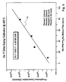
- Fig. 5 is a graph of the phosphorus concentration (atoms/cc) versus 100 PPM PH 3 /He mixture flow (SCCM).
- the ordinate represents phosphorus concentration (atoms/cc) and the abscissa represents flow (SCCM).
- the SIMS result shown in Fig. 4 gives a dopant profile width of about 150-200 ⁇ (15-20nm) at full width half maximum (FWHM).
- Hall measurements were used to measure and profile the active carriers throughout the doped sample by stepwise etching through the entire doped structure coupled with direct Hall measurement after each etching step.
- Fig. 6 is a graph showing the conductance versus depth and showing the phosphorus concentration versus depth in a multilayered structure using direct Hall measurements.
- the ordinate on the left side represents conductance (mS) and the abscissa represents depth below the surface of a multilayered Si 1-X Ge X structure having a layer of 1-2 nm Ge at a depth of 115 nm.
- Curve 80 shows the conductance as measured versus depth. The conductance increases from 0 at 120 nm to 0.21 at 110 nm. The dopant profile as measured by the electrical measurement is shown by curve 88. Curve 80 and/or its data points were used to generate curve 88 shown in Fig. 6 which shows the actual phosphorus doping profile.
- Curve 88 was generated by dividing the carrier density as determined from the conductance shown by curve 80 at the respective etched depth by the etch layer thickness.
- the ordinate on the right side represents P concentration (atoms/cc).
- Curve 86 shows the projected concentration based on curve 88 which shows the peak concentration rising abruptly from less than 1 X 10 15 at 121 nm to 5 X 10 19 at 115 nm corresponding to a 13 ⁇ (1.3nm) per decade rise in P concentration.
- the FWHM based on curve 86 which itself is projected from curve 88 is 8 nm at a peak concentration of 2 X 10 19 atoms/cc.
- the doping concentration as shown by curve 86 decreases from 5 X 10 19 atoms/cc at 115 nm to about 8 X 10 17 atoms/cc at 109 nm and 1 X 10 17 atoms/cc at 64.9 nm.
- the decrease in P concentration from 115 nm to 64.9 nm corresponds to a 20 nm per decade fall or decrease in P concentration.
- PH 3 has a sticking coefficient S of 1.0 while SiH 4 has a sticking coefficient S of 1 X 10 -3 to 1 X 10 -4 .
- the doping profile of P is a function of 1/GR where GR is the growth rate of the film.
- a growth interrupt method is provided.
- the substrates or wafers are removed from the growth chamber or UHV-CVD to another vacuum chamber such as a load lock or transfer chamber or another UHV-CVD reactor or furnace where no PH 3 has been flown prior to loading.
- SiH 4 and GeH 4 gases are flown in the growth chamber to coat the walls or heated surfaces of the growth chamber to bury or to isolate the P on the sidewalls.
- the substrates or wafers are introduced or moved back into the main or growth chamber and the growth of Si or Si 1-X Ge X is continued.
- another UHV-CVD reactor or furnace coupled to the transfer chamber may be used to continue the growth of Si or SiGe with reduced or no P or As doping.
- first epitaxial layer 80 is grown in the range from 1 to 10 nm thick of Si 1-X Ge X on a substrate 82 as shown in Fig. 7.
- First epitaxial layer 80 may be unstrained or a strained layer due to lattice mismatch with respect to substrate 82.
- a second epitaxial layer 84 may be grown over first epitaxial layer 80.
- Layer 84 may be Si or SiGe and may be unstrained or strained. Then using ion implantation shown in Fig.
- the first epitaxial layer 80 may be selectively amorphized to form layer 80' shown in Fig. 8 by ions 83 with respect to layer 84 and substrate 82 at a dose in the range from about 10 13 to about 10 14 atoms/cm 2 or higher; layer 84 and any other Si or SiGe layers will not be amorphized.
- the Ge content of layer 84 and the other layers should be less than the content X in layer 80.
- the critical dose for amorphization depends on the implanted species as well as on the host lattice. For example, boron does not amorphize Si at any dose, but amorphizes Ge at a dose higher than 1 X 10 14 atoms/cm 2 . Arsenic amorphizes Si at a dose of about 5 X 10 14 atoms/cm 2 , while arsenic amorphizes Ge at a dose of 1 X 10 13 atoms/cm 2 . Thus if an implant dose below the amorphization threshold in Si but above that in SiGe or Ge is used, then only the SiGe or Ge will be amorphized. The dossage peak should be adjusted to occur at the depth of the layer to be amorphized, layer 80.
- Substrate 82 and first epitaxial layer 80 is then heated to a temperature in the range from 400°C to 500° for a period of time such as from 1 to 5 hours which results in solid phase recrystallization of the amorphized layer to form Si 1-X Ge X layer 80" shown in Fig. 9.
- Recrystallization of amorphous layer 80' is dependent upon the material of the layer.
- Amorphous Ge recrystallizes at a temperature T greater than 350°C, while Si recrystallizes at a temperature T greater than 500°C.
- the combination of amorphization threshold dose and recrystallization temperature difference between Si and Ge is key to provide recrystallized layers.
- the alloy SiGe recrystallization temperature will be somewhere in between Si and Ge, depending on the Ge content. If thicker doped layers are sought, which are above the critical thickness of Ge on Si, then SiGe with the highest possible Ge content (that will stay strained) should be used. To maximize the sharpness of the doping profile, the layers surrounding the doped layer should have the lowest possible Ge content (depending on the design).
- Dopant activation occurs only in layer 80".
- the doped layer thickness 80" is determined by the original epitaxial layer thickness 80. Diffusion of P dopants at the recrystallization temperature is negligible.
- An n or p channel field effect transistor 91 is shown in Fig. 9 utilizing layer 80".
- a dielectric layer 85 may be formed on the upper surface of layer 84 to form a gate dielectric such as silicon dioxide.
- a gate 86 may be blanket deposited and patterned above dielectric 85 which may be polysilicon.
- Self aligned shallow souce and drain regions 87 and 88 may be formed in layer 84 by ion implantation using gate 86 as a mask.
- Sidewall spacers 89 and 90 may be formed on the sidewalls of gate 86.
- Source and drain regions 87' and 88' may be formed in layers 80 and 84 and substrate 82 using sidewall spacers 89 and 90 as a mask.
- Source 87 and 87' and drain 88 and 88' may be of one type material (n or p) and layer 80" may be of the opposite type material.
- Layer 80" functions to adjust the threshold voltage of the field effect transistor 91, prevent short channnel effects and prevent punch through between source and drain.
- a substrate 95 may be relaxed undoped SiGe.
- a phosphorous-doped Ge layer 96 is formed thereover as described with reference to Figs. 3 and 9.
- An undoped SiGe layer 97 is formed over layer 96.
- a strained undoped Si layer 98 may be formed over layer 97.
- Layer 98 is suitable for an electron or hole gas 99 to be present under proper voltage biasing conditions.
- field effect transistor 102 is shown.
- Source and drain regions 103 and 104 are formed spaced apart through layers 96-98 and into substrate 95.
- a gate dielectric 105 may be formed over layer 98 in the region between source 103 and drain 104.
- a gate electrode 106 of polysilicon or metal may be blanket deposited and patterned. Alternately, gate dielectric 105 may be deleted and a gate electrode of metal may form a Schottky barrier with layer 98.
- a cross section view of field effect transistor 110 is shown with raised source 40' and drain 40".
- Substrate 82' has a layer of field oxide 112 thereover with an opening 113 formed therein.
- a gate dielectric 85 is formed on substrate 82'.
- a gate electrode 86 is formed such as from polysilicon and a shallow source 87 and drain 88 are formed by, for example, ion implantation self aligned with respect to gate electrode 86.
- sidewalls 89 and 90 are formed on either side of gate electrode 86.
- a layer 36' is selectively formed epitaxially on shallow source 87 and drain 88 on substrate 82'which is phosphorous or arsenic doped.
- Layer 36' is Ge or substantially Ge and corresponds to layer 36 in Fig. 3.
- layer 40' of Si or SiGe is selectively formed epitaxially which is phosphorous or arsenic doped during fabrication.
- Layer 40' forms source 117 above shallow source 87 and forms drain 118 above shallow drain 88.
- Metal silicide contacts (not shown) may be made to source 117 and drain 118.
Landscapes
- Insulated Gate Type Field-Effect Transistor (AREA)
- Recrystallisation Techniques (AREA)
- Junction Field-Effect Transistors (AREA)
Abstract
Description
Claims (25)
- A structure having an abrupt doping profile comprising:a single crystal semiconductor substrate (32) having an upper surface,a first epitaxial layer (36) of Ge over said upper surface, said first epitaxial layer having a thickness less than the critical thickness, and having a concentration of dopant greater than 5 X 10¹⁹ atoms/cc, said dopant being selected from the group consisting of phosphorus and arsenic, anda second epitaxial layer (40) of a semiconductor material over said first epitaxial layer.
- The structure of claim 1 wherein said second layer comprises a material selected from the group consisting of Si and SiGe.
- The structure of claim 1 or 2 wherein said first layer has a thickness in the range from 0.5 to 2 nm.
- The structure of any preceding claim wherein said second layer has a concentration change from said first layer into 40Å (4nm) of said second layer of greater than 1 X 10¹⁹ atoms/cc.
- The structure of any preceding claim further including a third epitaxial layer of semiconductor material having a doping profile with a dopant concentration less than 5 X 10¹⁸ atoms/cc.
- The structure of any preceding claim wherein said second epitaxial layer has a thickness of at least 300Å (30nm) and has a doping of phosporus less than 5 X 10¹⁶ atoms/cc for a predetermined thickness after its initial 300Å (30nm) thickness.
- A method for forming an abrupt doping profile comprising the steps of:providing a single crystal semiconductor substrate having a major upper surface,forming a first epitaxial layer of Ge over said upper surface, said first epitaxial layer having a thickness less than the critical thickness,said step of forming the first epitaxial layer including the step of incorporating a concentration of dopant greater than 5 X 10¹⁹ atoms/cc, said dopant being selected from the group consisting of phosphorus and arsenic, andforming a second epitaxial layer of a semiconductor material over said first epitaxial layer.
- The method of claim 7 wherein said step of providing comprises providing a plurality of substrates, each substrate having a major upper surface, and wherein said steps of forming said first and second epitaxial layers are performed with respect to said plurality of substrates.
- The method of claim 7 or 8 wherein said step of forming said first epitaxial layer further includes the steps of placing said substrate in a CVD reactor and flowing a germanium containing gas and a dopant containing gas.
- The method of any of claims 7-9 wherein said step of forming said first epitaxial layer further includes the step of adjusting the growth rate of said first epitaxial layer as a function of time.
- The method of claim 10 as dependent on claim 9, wherein said step of adjusting the growth rate further includes the step of changing the flow rate of said germanium containing gas.
- The method of any of claims 7-11, wherein said step of forming said first epitaxial layer is terminated prior to reaching the critical thickness of said first epitaxial layer.
- The method of any of claims 7-12 wherein said step of forming said second epitaxial layer further includes the steps of placing said substrate in a CVD reactor and flowing a silicon containing gas and a dopant containing gas, said dopant being selected from the group consisting of phosphorus and arsenic.
- The method of claim 13 wherein said step of forming said second epitaxial layer further includes the step of adjusting the flow rate of said dopant containing gas as a function of time.
- The method of claim 13 or 14, wherein said step of forming said second epitaxial layer includes after the step of forming said first epitaxial layer, the steps of removing said substrate from said first CVD reactor to a load lock having a controlled atmosphere to prevent oxidation of the surface of said layer, and transferring said substrate to a second CVD reactor having internally exposed surfaces initially free of phosphorus.
- The method of claim 13 or 14, wherein said step of forming said second epitaxial layer includes the steps of:removing said substrate from said the CVD reactor to a load lock having a controlled atmosphere to prevent oxidation of the surface of said layer;flowing a silicon containing gas into the CVD having heated surfaces to coat said heated surfaces with a third silicon containing layer to cover said heated surfaces that may contain phosphorus containing layers that may have formed during the formation of said first epitaxial layer;transferring said substrate back into the CVD reactor, andforming a fourth layer on the upper surface of said second epitaxial layer.
- The method of claim 16 wherein said step of flowing a silicon containing gas includes the step of flowing the combination of H2/SiH4/GeH4.
- A method for forming abrupt doping within a semiconductor layered structure comprising the steps of:selectively amorphizing a first layer having a high Ge content greater than 0.5, andcrystallizing said amorphized first layer by solid phase regrowth.
- The method of claim 18 wherein said step of selectively amorphizing includes the step of ion implantation.
- The method of claim 18 or 19 wherein said step of selectively amorphizing includes forming second and third layers above said first layer, said second and third layers having a Ge content less than 0.5.
- A field effect transistor (91) comprising:a single crystal substrate (82) having a source region (87) and a drain region (88) with a channel therebetween and a gate electrode (86) above said channel to control charge in said channel, anda first layer of Ge (80") less than the critical thickness doped with a dopant selected from the group consisting of phosphorus and arsenic positioned below said channel and extending through said source and drain regions.
- The field effect transistor of claim 21 wherein said channel is in a second epitaxial layer selected from the group consisting of Si and SiGe formed over said first layer.
- A field effect transistor (102) comprising:a single crystal substrate (95),a first layer (96) of Ge less than the critical thickness doped with a dopant selected from the group consisting of phosphorus and arsenic formed on said substrate,a second layer (97) of undoped SiGe epitaxially formed on said first layer,a third layer (98) of strained undoped semiconductor material selected from the group consisting of Si and SiGe, anda source region (103) and a drain region (104) with a channel therebetween, and a gate electrode (106) above said channel to control charge in said channel.
- A field effect transistor (110) comprising:a single crystal substrate (82),an oxide layer (112) formed on said substrate having an opening (113),a gate dielectric (85) and gate electrode (86) formed in said opening over said substrate,a source and drain region (117, 118) formed in said substrate aligned with respect to said gate electrode,a dielectric sidewall spacer (89, 90) formed on either side of said gate electrode and above a portion of said source and drain regions,a first layer (36') of Ge less than the critical thickness doped with a dopant selected from the group consisting of phosphorus and arsenic selectively positioned over exposed portions of said source and drain regions,a second layer (40') of semiconductor material selected from the group consisting of Si and SiGe doped with a dopant selected from the group consisting of phosphorus and arsenic epitaxially formed over said first layer to form raised source and drain regions.
- The field effect transistor of any of claims 21 to 24 wherein said layer of Ge is in the range from 0.5 to 2 nm thick.
Applications Claiming Priority (2)
| Application Number | Priority Date | Filing Date | Title |
|---|---|---|---|
| US08/885,611 US6723621B1 (en) | 1997-06-30 | 1997-06-30 | Abrupt delta-like doping in Si and SiGe films by UHV-CVD |
| US885611 | 1997-06-30 |
Publications (3)
| Publication Number | Publication Date |
|---|---|
| EP0889502A2 true EP0889502A2 (en) | 1999-01-07 |
| EP0889502A3 EP0889502A3 (en) | 2000-06-28 |
| EP0889502B1 EP0889502B1 (en) | 2006-12-20 |
Family
ID=25387309
Family Applications (1)
| Application Number | Title | Priority Date | Filing Date |
|---|---|---|---|
| EP98305045A Expired - Lifetime EP0889502B1 (en) | 1997-06-30 | 1998-06-26 | Semiconductor structure with abrupt doping profile |
Country Status (6)
| Country | Link |
|---|---|
| US (3) | US6723621B1 (en) |
| EP (1) | EP0889502B1 (en) |
| JP (1) | JP3083802B2 (en) |
| KR (1) | KR100275397B1 (en) |
| DE (1) | DE69836654T2 (en) |
| TW (1) | TW376570B (en) |
Cited By (34)
| Publication number | Priority date | Publication date | Assignee | Title |
|---|---|---|---|---|
| GB2355583A (en) * | 1999-06-29 | 2001-04-25 | Hyundai Electronics Ind | Method of forming a transistor having elevated source and drain regions |
| DE10034942A1 (en) * | 2000-07-12 | 2002-01-31 | Infineon Technologies Ag | Method for producing a doped semiconductor substrate |
| WO2003034480A1 (en) * | 2001-10-18 | 2003-04-24 | Applied Materials, Inc. | Low energy ion implantation into sige |
| WO2003025984A3 (en) * | 2001-09-21 | 2003-09-25 | Amberwave Systems Corp | Semiconductor structures employing strained material layers with defined impurity gradients and methods for fabricating same |
| EP1231643A3 (en) * | 2001-02-09 | 2004-10-06 | President of Tohoku University | MOS field-effect transistor comprising Si and SiGe layers or Si and SiGeC layers as channel regions |
| WO2007027473A3 (en) * | 2005-08-31 | 2007-04-19 | Advanced Micro Devices Inc | Technique for forming recessed strained drain/source in nmos and pmos transistors |
| EP1447839A4 (en) * | 2001-08-06 | 2009-11-04 | Sumco Corp | SEMICONDUCTOR SUBSTRATE, FIELD EFFECT TRANSISTOR, AND METHODS OF MAKING THE SAME |
| EP1592048A4 (en) * | 2003-02-04 | 2011-03-02 | Sumco Corp | SEMICONDUCTOR SUBSTRATE, FIELD EFFECT TRANSISTOR AND METHODS OF PRODUCING THE SAME |
| US7923339B2 (en) | 2004-12-06 | 2011-04-12 | Nxp B.V. | Method of producing an epitaxial layer on semiconductor substrate and device produced with such a method |
| US8599623B1 (en) | 2011-12-23 | 2013-12-03 | Suvolta, Inc. | Circuits and methods for measuring circuit elements in an integrated circuit device |
| US8748986B1 (en) | 2011-08-05 | 2014-06-10 | Suvolta, Inc. | Electronic device with controlled threshold voltage |
| US8811068B1 (en) | 2011-05-13 | 2014-08-19 | Suvolta, Inc. | Integrated circuit devices and methods |
| US8816754B1 (en) | 2012-11-02 | 2014-08-26 | Suvolta, Inc. | Body bias circuits and methods |
| US8819603B1 (en) | 2011-12-15 | 2014-08-26 | Suvolta, Inc. | Memory circuits and methods of making and designing the same |
| US8895327B1 (en) | 2011-12-09 | 2014-11-25 | Suvolta, Inc. | Tipless transistors, short-tip transistors, and methods and circuits therefor |
| US8970289B1 (en) | 2012-01-23 | 2015-03-03 | Suvolta, Inc. | Circuits and devices for generating bi-directional body bias voltages, and methods therefor |
| US8995204B2 (en) | 2011-06-23 | 2015-03-31 | Suvolta, Inc. | Circuit devices and methods having adjustable transistor body bias |
| US9070477B1 (en) | 2012-12-12 | 2015-06-30 | Mie Fujitsu Semiconductor Limited | Bit interleaved low voltage static random access memory (SRAM) and related methods |
| US9093997B1 (en) | 2012-11-15 | 2015-07-28 | Mie Fujitsu Semiconductor Limited | Slew based process and bias monitors and related methods |
| US9112484B1 (en) | 2012-12-20 | 2015-08-18 | Mie Fujitsu Semiconductor Limited | Integrated circuit process and bias monitors and related methods |
| US9236466B1 (en) | 2011-10-07 | 2016-01-12 | Mie Fujitsu Semiconductor Limited | Analog circuits having improved insulated gate transistors, and methods therefor |
| US9268885B1 (en) | 2013-02-28 | 2016-02-23 | Mie Fujitsu Semiconductor Limited | Integrated circuit device methods and models with predicted device metric variations |
| US9319013B2 (en) | 2014-08-19 | 2016-04-19 | Mie Fujitsu Semiconductor Limited | Operational amplifier input offset correction with transistor threshold voltage adjustment |
| US9431068B2 (en) | 2012-10-31 | 2016-08-30 | Mie Fujitsu Semiconductor Limited | Dynamic random access memory (DRAM) with low variation transistor peripheral circuits |
| US9680470B2 (en) | 2011-02-18 | 2017-06-13 | Mie Fujitsu Semiconductor Limited | Digital circuits having improved transistors, and methods therefor |
| US9710006B2 (en) | 2014-07-25 | 2017-07-18 | Mie Fujitsu Semiconductor Limited | Power up body bias circuits and methods |
| US9786703B2 (en) | 2013-05-24 | 2017-10-10 | Mie Fujitsu Semiconductor Limited | Buried channel deeply depleted channel transistor |
| US9793172B2 (en) | 2011-05-16 | 2017-10-17 | Mie Fujitsu Semiconductor Limited | Reducing or eliminating pre-amorphization in transistor manufacture |
| US9812550B2 (en) | 2012-06-27 | 2017-11-07 | Mie Fujitsu Semiconductor Limited | Semiconductor structure with multiple transistors having various threshold voltages |
| US9865596B2 (en) | 2010-04-12 | 2018-01-09 | Mie Fujitsu Semiconductor Limited | Low power semiconductor transistor structure and method of fabrication thereof |
| US9893148B2 (en) | 2013-03-14 | 2018-02-13 | Mie Fujitsu Semiconductor Limited | Method for fabricating a transistor device with a tuned dopant profile |
| US9922977B2 (en) | 2010-06-22 | 2018-03-20 | Mie Fujitsu Semiconductor Limited | Transistor with threshold voltage set notch and method of fabrication thereof |
| US10074568B2 (en) | 2009-09-30 | 2018-09-11 | Mie Fujitsu Semiconductor Limited | Electronic devices and systems, and methods for making and using same |
| US10325986B2 (en) | 2009-09-30 | 2019-06-18 | Mie Fujitsu Semiconductor Limited | Advanced transistors with punch through suppression |
Families Citing this family (74)
| Publication number | Priority date | Publication date | Assignee | Title |
|---|---|---|---|---|
| US7145167B1 (en) * | 2000-03-11 | 2006-12-05 | International Business Machines Corporation | High speed Ge channel heterostructures for field effect devices |
| DE60125338T2 (en) * | 2000-03-07 | 2007-07-05 | Asm International N.V. | GRADED THIN LAYERS |
| DE10025264A1 (en) * | 2000-05-22 | 2001-11-29 | Max Planck Gesellschaft | Field effect transistor based on embedded cluster structures and method for its production |
| US6555839B2 (en) * | 2000-05-26 | 2003-04-29 | Amberwave Systems Corporation | Buried channel strained silicon FET using a supply layer created through ion implantation |
| US6495402B1 (en) * | 2001-02-06 | 2002-12-17 | Advanced Micro Devices, Inc. | Semiconductor-on-insulator (SOI) device having source/drain silicon-germanium regions and method of manufacture |
| US6830976B2 (en) | 2001-03-02 | 2004-12-14 | Amberwave Systems Corproation | Relaxed silicon germanium platform for high speed CMOS electronics and high speed analog circuits |
| US6703688B1 (en) * | 2001-03-02 | 2004-03-09 | Amberwave Systems Corporation | Relaxed silicon germanium platform for high speed CMOS electronics and high speed analog circuits |
| AU2002341803A1 (en) | 2001-09-24 | 2003-04-07 | Amberwave Systems Corporation | Rf circuits including transistors having strained material layers |
| JP3873012B2 (en) * | 2002-07-29 | 2007-01-24 | 株式会社東芝 | Manufacturing method of semiconductor device |
| DE60334723D1 (en) * | 2002-11-19 | 2010-12-09 | Univ Rice William M | Field effect transistor with functionalized carbon nanotube and its manufacturing process |
| US6809016B1 (en) * | 2003-03-06 | 2004-10-26 | Advanced Micro Devices, Inc. | Diffusion stop implants to suppress as punch-through in SiGe |
| US7598513B2 (en) * | 2003-06-13 | 2009-10-06 | Arizona Board Of Regents, Acting For And On Behalf Of Arizona State University, A Corporate Body Organized Under Arizona Law | SixSnyGe1-x-y and related alloy heterostructures based on Si, Ge and Sn |
| WO2005001902A2 (en) * | 2003-06-13 | 2005-01-06 | Arizona Board Of Regents, Acting For And On Behalf Of Arizona State University | Gesn alloys and ordered phases with direct tunable bandgaps grown directly on silicon |
| US7589003B2 (en) * | 2003-06-13 | 2009-09-15 | Arizona Board Of Regents, Acting For And On Behalf Of Arizona State University, A Corporate Body Organized Under Arizona Law | GeSn alloys and ordered phases with direct tunable bandgaps grown directly on silicon |
| US20050054164A1 (en) * | 2003-09-09 | 2005-03-10 | Advanced Micro Devices, Inc. | Strained silicon MOSFETs having reduced diffusion of n-type dopants |
| US7202145B2 (en) * | 2004-06-03 | 2007-04-10 | Taiwan Semiconductor Manufacturing Company | Strained Si formed by anneal |
| US7320931B2 (en) * | 2004-07-30 | 2008-01-22 | Freescale Semiconductor Inc. | Interfacial layer for use with high k dielectric materials |
| KR101131418B1 (en) * | 2004-12-07 | 2012-04-03 | 주성엔지니어링(주) | Semiconductor device and manufacturing method thereof |
| KR100613355B1 (en) * | 2004-12-30 | 2006-08-21 | 동부일렉트로닉스 주식회사 | MOS field effect transistor and its manufacturing method |
| US7892915B1 (en) * | 2006-03-02 | 2011-02-22 | National Semiconductor Corporation | High performance SiGe:C HBT with phosphorous atomic layer doping |
| US7485538B1 (en) * | 2006-03-27 | 2009-02-03 | National Semiconductor Corporation | High performance SiGe HBT with arsenic atomic layer doping |
| KR100793607B1 (en) | 2006-06-27 | 2008-01-10 | 매그나칩 반도체 유한회사 | Epitaxial Silicon Wafers and Manufacturing Method Thereof |
| US7504301B2 (en) * | 2006-09-28 | 2009-03-17 | Advanced Micro Devices, Inc. | Stressed field effect transistor and methods for its fabrication |
| US20080086069A1 (en) * | 2006-10-10 | 2008-04-10 | Robert Busuttil | Wrist support brace |
| US20090062707A1 (en) * | 2007-09-04 | 2009-03-05 | Robert Busuttil | Wrist support brace |
| EP2267782A3 (en) | 2009-06-24 | 2013-03-13 | Imec | Control of tunneling junction in a hetero tunnel field effect transistor |
| CN101673673B (en) * | 2009-09-22 | 2013-02-27 | 上海宏力半导体制造有限公司 | Method for forming epitaxial wafer and epitaxial wafer formed by using same |
| US20110079861A1 (en) * | 2009-09-30 | 2011-04-07 | Lucian Shifren | Advanced Transistors with Threshold Voltage Set Dopant Structures |
| US8283653B2 (en) | 2009-12-23 | 2012-10-09 | Intel Corporation | Non-planar germanium quantum well devices |
| CN101777498A (en) * | 2010-01-12 | 2010-07-14 | 上海宏力半导体制造有限公司 | Method for forming epitaxial wafer with superficial epitaxial layer and epitaxial wafer thereof |
| US8569128B2 (en) | 2010-06-21 | 2013-10-29 | Suvolta, Inc. | Semiconductor structure and method of fabrication thereof with mixed metal types |
| JP5269010B2 (en) * | 2010-08-17 | 2013-08-21 | 株式会社東芝 | Nonvolatile semiconductor memory device |
| US8377783B2 (en) | 2010-09-30 | 2013-02-19 | Suvolta, Inc. | Method for reducing punch-through in a transistor device |
| CN102468303B (en) * | 2010-11-10 | 2015-05-13 | 中国科学院微电子研究所 | Semiconductor memory cell, device and preparation method thereof |
| US8404551B2 (en) | 2010-12-03 | 2013-03-26 | Suvolta, Inc. | Source/drain extension control for advanced transistors |
| US8525271B2 (en) | 2011-03-03 | 2013-09-03 | Suvolta, Inc. | Semiconductor structure with improved channel stack and method for fabrication thereof |
| US8400219B2 (en) | 2011-03-24 | 2013-03-19 | Suvolta, Inc. | Analog circuits having improved transistors, and methods therefor |
| US8748270B1 (en) | 2011-03-30 | 2014-06-10 | Suvolta, Inc. | Process for manufacturing an improved analog transistor |
| US8338279B2 (en) | 2011-03-30 | 2012-12-25 | International Business Machines Corporation | Reduced pattern loading for doped epitaxial process and semiconductor structure |
| US8796048B1 (en) | 2011-05-11 | 2014-08-05 | Suvolta, Inc. | Monitoring and measurement of thin film layers |
| US8999861B1 (en) | 2011-05-11 | 2015-04-07 | Suvolta, Inc. | Semiconductor structure with substitutional boron and method for fabrication thereof |
| US8735987B1 (en) | 2011-06-06 | 2014-05-27 | Suvolta, Inc. | CMOS gate stack structures and processes |
| US9692209B2 (en) | 2011-06-10 | 2017-06-27 | Massachusetts Institute Of Technology | High-concentration active doping in semiconductors and semiconductor devices produced by such doping |
| US8629016B1 (en) | 2011-07-26 | 2014-01-14 | Suvolta, Inc. | Multiple transistor types formed in a common epitaxial layer by differential out-diffusion from a doped underlayer |
| KR101891373B1 (en) | 2011-08-05 | 2018-08-24 | 엠아이이 후지쯔 세미컨덕터 리미티드 | Semiconductor devices having fin structures and fabrication methods thereof |
| US8994123B2 (en) | 2011-08-22 | 2015-03-31 | Gold Standard Simulations Ltd. | Variation resistant metal-oxide-semiconductor field effect transistor (MOSFET) |
| US8614128B1 (en) | 2011-08-23 | 2013-12-24 | Suvolta, Inc. | CMOS structures and processes based on selective thinning |
| US8645878B1 (en) | 2011-08-23 | 2014-02-04 | Suvolta, Inc. | Porting a circuit design from a first semiconductor process to a second semiconductor process |
| US8713511B1 (en) | 2011-09-16 | 2014-04-29 | Suvolta, Inc. | Tools and methods for yield-aware semiconductor manufacturing process target generation |
| US8883600B1 (en) | 2011-12-22 | 2014-11-11 | Suvolta, Inc. | Transistor having reduced junction leakage and methods of forming thereof |
| CN104737268A (en) * | 2012-01-12 | 2015-06-24 | 第一太阳能有限公司 | Method and system for providing dopant concentration control in different layers of a semiconductor device |
| US8877619B1 (en) | 2012-01-23 | 2014-11-04 | Suvolta, Inc. | Process for manufacture of integrated circuits with different channel doping transistor architectures and devices therefrom |
| US9093550B1 (en) | 2012-01-31 | 2015-07-28 | Mie Fujitsu Semiconductor Limited | Integrated circuits having a plurality of high-K metal gate FETs with various combinations of channel foundation structure and gate stack structure and methods of making same |
| US9406567B1 (en) | 2012-02-28 | 2016-08-02 | Mie Fujitsu Semiconductor Limited | Method for fabricating multiple transistor devices on a substrate with varying threshold voltages |
| US9373684B2 (en) | 2012-03-20 | 2016-06-21 | Semiwise Limited | Method of manufacturing variation resistant metal-oxide-semiconductor field effect transistor (MOSFET) |
| US8863064B1 (en) | 2012-03-23 | 2014-10-14 | Suvolta, Inc. | SRAM cell layout structure and devices therefrom |
| US9269804B2 (en) | 2012-07-28 | 2016-02-23 | Semiwise Limited | Gate recessed FDSOI transistor with sandwich of active and etch control layers |
| US9190485B2 (en) | 2012-07-28 | 2015-11-17 | Gold Standard Simulations Ltd. | Fluctuation resistant FDSOI transistor with implanted subchannel |
| US9263568B2 (en) | 2012-07-28 | 2016-02-16 | Semiwise Limited | Fluctuation resistant low access resistance fully depleted SOI transistor with improved channel thickness control and reduced access resistance |
| US8637955B1 (en) | 2012-08-31 | 2014-01-28 | Suvolta, Inc. | Semiconductor structure with reduced junction leakage and method of fabrication thereof |
| US9112057B1 (en) | 2012-09-18 | 2015-08-18 | Mie Fujitsu Semiconductor Limited | Semiconductor devices with dopant migration suppression and method of fabrication thereof |
| US9041126B2 (en) | 2012-09-21 | 2015-05-26 | Mie Fujitsu Semiconductor Limited | Deeply depleted MOS transistors having a screening layer and methods thereof |
| US8994415B1 (en) | 2013-03-01 | 2015-03-31 | Suvolta, Inc. | Multiple VDD clock buffer |
| US8988153B1 (en) | 2013-03-09 | 2015-03-24 | Suvolta, Inc. | Ring oscillator with NMOS or PMOS variation insensitivity |
| US9449967B1 (en) | 2013-03-15 | 2016-09-20 | Fujitsu Semiconductor Limited | Transistor array structure |
| US9112495B1 (en) | 2013-03-15 | 2015-08-18 | Mie Fujitsu Semiconductor Limited | Integrated circuit device body bias circuits and methods |
| US9012276B2 (en) | 2013-07-05 | 2015-04-21 | Gold Standard Simulations Ltd. | Variation resistant MOSFETs with superior epitaxial properties |
| US8976575B1 (en) | 2013-08-29 | 2015-03-10 | Suvolta, Inc. | SRAM performance monitor |
| US9716160B2 (en) * | 2014-08-01 | 2017-07-25 | International Business Machines Corporation | Extended contact area using undercut silicide extensions |
| US11049939B2 (en) | 2015-08-03 | 2021-06-29 | Semiwise Limited | Reduced local threshold voltage variation MOSFET using multiple layers of epi for improved device operation |
| JP2017139312A (en) * | 2016-02-03 | 2017-08-10 | 株式会社Screenホールディングス | Junction formation method |
| US10276663B2 (en) * | 2016-07-18 | 2019-04-30 | United Microelectronics Corp. | Tunneling transistor and method of fabricating the same |
| US11373696B1 (en) | 2021-02-19 | 2022-06-28 | Nif/T, Llc | FFT-dram |
| KR20260116023A (en) * | 2023-12-01 | 2026-07-27 | 유미코아 | Ultra-highly doped N-type germanium single crystal and wafer derived therefrom |
Family Cites Families (20)
| Publication number | Priority date | Publication date | Assignee | Title |
|---|---|---|---|---|
| US5607511A (en) * | 1992-02-21 | 1997-03-04 | International Business Machines Corporation | Method and apparatus for low temperature, low pressure chemical vapor deposition of epitaxial silicon layers |
| US5298452A (en) * | 1986-09-12 | 1994-03-29 | International Business Machines Corporation | Method and apparatus for low temperature, low pressure chemical vapor deposition of epitaxial silicon layers |
| JPS63168021A (en) | 1986-12-29 | 1988-07-12 | Nec Corp | Polycrystalline sige thin film |
| US4863877A (en) * | 1987-11-13 | 1989-09-05 | Kopin Corporation | Ion implantation and annealing of compound semiconductor layers |
| JP2764966B2 (en) * | 1988-03-25 | 1998-06-11 | 日本電気株式会社 | Heterostructure bipolar transistor and molecular beam epitaxy. |
| US5241197A (en) * | 1989-01-25 | 1993-08-31 | Hitachi, Ltd. | Transistor provided with strained germanium layer |
| JP2695466B2 (en) | 1989-04-28 | 1997-12-24 | キヤノン株式会社 | Crystal growth method |
| US5227644A (en) | 1989-07-06 | 1993-07-13 | Nec Corporation | Heterojunction field effect transistor with improve carrier density and mobility |
| US5089428A (en) * | 1989-12-27 | 1992-02-18 | Texas Instruments Incorporated | Method for forming a germanium layer and a heterojunction bipolar transistor |
| US5628834A (en) * | 1990-03-23 | 1997-05-13 | International Business Machines Corporation | Surfactant-enhanced epitaxy |
| US5316958A (en) | 1990-05-31 | 1994-05-31 | International Business Machines Corporation | Method of dopant enhancement in an epitaxial silicon layer by using germanium |
| US5181964A (en) * | 1990-06-13 | 1993-01-26 | International Business Machines Corporation | Single ended ultra-high vacuum chemical vapor deposition (uhv/cvd) reactor |
| JPH0691249B2 (en) | 1991-01-10 | 1994-11-14 | インターナショナル・ビジネス・マシーンズ・コーポレイション | Modulation-doped MISFET and manufacturing method thereof |
| CA2062134C (en) * | 1991-05-31 | 1997-03-25 | Ibm | Heteroepitaxial layers with low defect density and arbitrary network parameter |
| KR100274555B1 (en) * | 1991-06-26 | 2000-12-15 | 윌리엄 비. 켐플러 | Insulated gate field effect transistor and manufacturing the same |
| JPH0661489A (en) | 1992-08-10 | 1994-03-04 | Sharp Corp | Method of manufacturing thin film transistor |
| JP2551364B2 (en) * | 1993-11-26 | 1996-11-06 | 日本電気株式会社 | Semiconductor device |
| US5466949A (en) * | 1994-08-04 | 1995-11-14 | Texas Instruments Incorporated | Silicon oxide germanium resonant tunneling |
| US6383899B1 (en) * | 1996-04-05 | 2002-05-07 | Sharp Laboratories Of America, Inc. | Method of forming polycrystalline semiconductor film from amorphous deposit by modulating crystallization with a combination of pre-annealing and ion implantation |
| JPH10288328A (en) | 1997-04-15 | 1998-10-27 | Nippon Steel Corp | Exhaust gas combustion tower |
-
1997
- 1997-06-30 US US08/885,611 patent/US6723621B1/en not_active Expired - Lifetime
-
1998
- 1998-04-21 TW TW087106046A patent/TW376570B/en not_active IP Right Cessation
- 1998-05-14 KR KR1019980017440A patent/KR100275397B1/en not_active Expired - Fee Related
- 1998-06-16 JP JP10168309A patent/JP3083802B2/en not_active Expired - Lifetime
- 1998-06-26 EP EP98305045A patent/EP0889502B1/en not_active Expired - Lifetime
- 1998-06-26 DE DE69836654T patent/DE69836654T2/en not_active Expired - Lifetime
-
2003
- 2003-12-12 US US10/735,167 patent/US7067855B2/en not_active Expired - Fee Related
-
2006
- 2006-04-28 US US11/414,091 patent/US7906413B2/en not_active Expired - Fee Related
Cited By (58)
| Publication number | Priority date | Publication date | Assignee | Title |
|---|---|---|---|---|
| GB2355583A (en) * | 1999-06-29 | 2001-04-25 | Hyundai Electronics Ind | Method of forming a transistor having elevated source and drain regions |
| GB2355583B (en) * | 1999-06-29 | 2004-04-14 | Hyundai Electronics Ind | Method of manufacturing a transistor having elevated source and drain regions |
| US7078325B2 (en) | 2000-07-12 | 2006-07-18 | Infineon Technologies Ag | Process for producing a doped semiconductor substrate |
| DE10034942A1 (en) * | 2000-07-12 | 2002-01-31 | Infineon Technologies Ag | Method for producing a doped semiconductor substrate |
| DE10034942B4 (en) * | 2000-07-12 | 2004-08-05 | Infineon Technologies Ag | Method for producing a semiconductor substrate with buried doping |
| EP1231643A3 (en) * | 2001-02-09 | 2004-10-06 | President of Tohoku University | MOS field-effect transistor comprising Si and SiGe layers or Si and SiGeC layers as channel regions |
| EP1447839A4 (en) * | 2001-08-06 | 2009-11-04 | Sumco Corp | SEMICONDUCTOR SUBSTRATE, FIELD EFFECT TRANSISTOR, AND METHODS OF MAKING THE SAME |
| WO2003025984A3 (en) * | 2001-09-21 | 2003-09-25 | Amberwave Systems Corp | Semiconductor structures employing strained material layers with defined impurity gradients and methods for fabricating same |
| US6831292B2 (en) | 2001-09-21 | 2004-12-14 | Amberwave Systems Corporation | Semiconductor structures employing strained material layers with defined impurity gradients and methods for fabricating same |
| US7884353B2 (en) | 2001-09-21 | 2011-02-08 | Taiwan Semiconductor Manufacturing Company, Ltd. | Semiconductor structures employing strained material layers with defined impurity gradients and methods for fabricating same |
| WO2003034480A1 (en) * | 2001-10-18 | 2003-04-24 | Applied Materials, Inc. | Low energy ion implantation into sige |
| EP1592048A4 (en) * | 2003-02-04 | 2011-03-02 | Sumco Corp | SEMICONDUCTOR SUBSTRATE, FIELD EFFECT TRANSISTOR AND METHODS OF PRODUCING THE SAME |
| US7923339B2 (en) | 2004-12-06 | 2011-04-12 | Nxp B.V. | Method of producing an epitaxial layer on semiconductor substrate and device produced with such a method |
| US7586153B2 (en) | 2005-08-31 | 2009-09-08 | Advanced Micro Devices, Inc. | Technique for forming recessed strained drain/source regions in NMOS and PMOS transistors |
| GB2444198B (en) * | 2005-08-31 | 2009-04-01 | Advanced Micro Devices Inc | Technique for forming recessed strained drain/source in NMOS and PMOS transistors |
| GB2444198A (en) * | 2005-08-31 | 2008-05-28 | Advanced Micro Devices Inc | Technique for forming recessed strained drain/source in NMOS and PMOS transistors |
| WO2007027473A3 (en) * | 2005-08-31 | 2007-04-19 | Advanced Micro Devices Inc | Technique for forming recessed strained drain/source in nmos and pmos transistors |
| US11887895B2 (en) | 2009-09-30 | 2024-01-30 | United Semiconductor Japan Co., Ltd. | Electronic devices and systems, and methods for making and using the same |
| US11062950B2 (en) | 2009-09-30 | 2021-07-13 | United Semiconductor Japan Co., Ltd. | Electronic devices and systems, and methods for making and using the same |
| US10325986B2 (en) | 2009-09-30 | 2019-06-18 | Mie Fujitsu Semiconductor Limited | Advanced transistors with punch through suppression |
| US10224244B2 (en) | 2009-09-30 | 2019-03-05 | Mie Fujitsu Semiconductor Limited | Electronic devices and systems, and methods for making and using the same |
| US10217668B2 (en) | 2009-09-30 | 2019-02-26 | Mie Fujitsu Semiconductor Limited | Electronic devices and systems, and methods for making and using the same |
| US10074568B2 (en) | 2009-09-30 | 2018-09-11 | Mie Fujitsu Semiconductor Limited | Electronic devices and systems, and methods for making and using same |
| US9865596B2 (en) | 2010-04-12 | 2018-01-09 | Mie Fujitsu Semiconductor Limited | Low power semiconductor transistor structure and method of fabrication thereof |
| US9922977B2 (en) | 2010-06-22 | 2018-03-20 | Mie Fujitsu Semiconductor Limited | Transistor with threshold voltage set notch and method of fabrication thereof |
| US9838012B2 (en) | 2011-02-18 | 2017-12-05 | Mie Fujitsu Semiconductor Limited | Digital circuits having improved transistors, and methods therefor |
| US10250257B2 (en) | 2011-02-18 | 2019-04-02 | Mie Fujitsu Semiconductor Limited | Digital circuits having improved transistors, and methods therefor |
| US9985631B2 (en) | 2011-02-18 | 2018-05-29 | Mie Fujitsu Semiconductor Limited | Digital circuits having improved transistors, and methods therefor |
| US9680470B2 (en) | 2011-02-18 | 2017-06-13 | Mie Fujitsu Semiconductor Limited | Digital circuits having improved transistors, and methods therefor |
| US9362291B1 (en) | 2011-05-13 | 2016-06-07 | Mie Fujitsu Semiconductor Limited | Integrated circuit devices and methods |
| US8811068B1 (en) | 2011-05-13 | 2014-08-19 | Suvolta, Inc. | Integrated circuit devices and methods |
| US9966130B2 (en) | 2011-05-13 | 2018-05-08 | Mie Fujitsu Semiconductor Limited | Integrated circuit devices and methods |
| US9741428B2 (en) | 2011-05-13 | 2017-08-22 | Mie Fujitsu Semiconductor Limited | Integrated circuit devices and methods |
| US9793172B2 (en) | 2011-05-16 | 2017-10-17 | Mie Fujitsu Semiconductor Limited | Reducing or eliminating pre-amorphization in transistor manufacture |
| US8995204B2 (en) | 2011-06-23 | 2015-03-31 | Suvolta, Inc. | Circuit devices and methods having adjustable transistor body bias |
| US8963249B1 (en) | 2011-08-05 | 2015-02-24 | Suvolta, Inc. | Electronic device with controlled threshold voltage |
| US8748986B1 (en) | 2011-08-05 | 2014-06-10 | Suvolta, Inc. | Electronic device with controlled threshold voltage |
| US9236466B1 (en) | 2011-10-07 | 2016-01-12 | Mie Fujitsu Semiconductor Limited | Analog circuits having improved insulated gate transistors, and methods therefor |
| US8895327B1 (en) | 2011-12-09 | 2014-11-25 | Suvolta, Inc. | Tipless transistors, short-tip transistors, and methods and circuits therefor |
| US8819603B1 (en) | 2011-12-15 | 2014-08-26 | Suvolta, Inc. | Memory circuits and methods of making and designing the same |
| US8599623B1 (en) | 2011-12-23 | 2013-12-03 | Suvolta, Inc. | Circuits and methods for measuring circuit elements in an integrated circuit device |
| US9297850B1 (en) | 2011-12-23 | 2016-03-29 | Mie Fujitsu Semiconductor Limited | Circuits and methods for measuring circuit elements in an integrated circuit device |
| US8970289B1 (en) | 2012-01-23 | 2015-03-03 | Suvolta, Inc. | Circuits and devices for generating bi-directional body bias voltages, and methods therefor |
| US10217838B2 (en) | 2012-06-27 | 2019-02-26 | Mie Fujitsu Semiconductor Limited | Semiconductor structure with multiple transistors having various threshold voltages |
| US10014387B2 (en) | 2012-06-27 | 2018-07-03 | Mie Fujitsu Semiconductor Limited | Semiconductor structure with multiple transistors having various threshold voltages |
| US9812550B2 (en) | 2012-06-27 | 2017-11-07 | Mie Fujitsu Semiconductor Limited | Semiconductor structure with multiple transistors having various threshold voltages |
| US9431068B2 (en) | 2012-10-31 | 2016-08-30 | Mie Fujitsu Semiconductor Limited | Dynamic random access memory (DRAM) with low variation transistor peripheral circuits |
| US9154123B1 (en) | 2012-11-02 | 2015-10-06 | Mie Fujitsu Semiconductor Limited | Body bias circuits and methods |
| US8816754B1 (en) | 2012-11-02 | 2014-08-26 | Suvolta, Inc. | Body bias circuits and methods |
| US9093997B1 (en) | 2012-11-15 | 2015-07-28 | Mie Fujitsu Semiconductor Limited | Slew based process and bias monitors and related methods |
| US9070477B1 (en) | 2012-12-12 | 2015-06-30 | Mie Fujitsu Semiconductor Limited | Bit interleaved low voltage static random access memory (SRAM) and related methods |
| US9112484B1 (en) | 2012-12-20 | 2015-08-18 | Mie Fujitsu Semiconductor Limited | Integrated circuit process and bias monitors and related methods |
| US9268885B1 (en) | 2013-02-28 | 2016-02-23 | Mie Fujitsu Semiconductor Limited | Integrated circuit device methods and models with predicted device metric variations |
| US9893148B2 (en) | 2013-03-14 | 2018-02-13 | Mie Fujitsu Semiconductor Limited | Method for fabricating a transistor device with a tuned dopant profile |
| US9991300B2 (en) | 2013-05-24 | 2018-06-05 | Mie Fujitsu Semiconductor Limited | Buried channel deeply depleted channel transistor |
| US9786703B2 (en) | 2013-05-24 | 2017-10-10 | Mie Fujitsu Semiconductor Limited | Buried channel deeply depleted channel transistor |
| US9710006B2 (en) | 2014-07-25 | 2017-07-18 | Mie Fujitsu Semiconductor Limited | Power up body bias circuits and methods |
| US9319013B2 (en) | 2014-08-19 | 2016-04-19 | Mie Fujitsu Semiconductor Limited | Operational amplifier input offset correction with transistor threshold voltage adjustment |
Also Published As
| Publication number | Publication date |
|---|---|
| US20040185640A1 (en) | 2004-09-23 |
| JPH1167666A (en) | 1999-03-09 |
| US7906413B2 (en) | 2011-03-15 |
| US7067855B2 (en) | 2006-06-27 |
| EP0889502B1 (en) | 2006-12-20 |
| KR19990006451A (en) | 1999-01-25 |
| US6723621B1 (en) | 2004-04-20 |
| JP3083802B2 (en) | 2000-09-04 |
| DE69836654D1 (en) | 2007-02-01 |
| DE69836654T2 (en) | 2007-09-27 |
| TW376570B (en) | 1999-12-11 |
| US20060194422A1 (en) | 2006-08-31 |
| KR100275397B1 (en) | 2000-12-15 |
| EP0889502A3 (en) | 2000-06-28 |
Similar Documents
| Publication | Publication Date | Title |
|---|---|---|
| EP0889502B1 (en) | Semiconductor structure with abrupt doping profile | |
| US9312131B2 (en) | Selective epitaxial formation of semiconductive films | |
| US6713359B1 (en) | Semiconductor device and method of manufacturing the same including raised source/drain comprising SiGe or SiC | |
| US7960236B2 (en) | Phosphorus containing Si epitaxial layers in N-type source/drain junctions | |
| US5731626A (en) | Process for controlling dopant diffusion in a semiconductor layer and semiconductor layer formed thereby | |
| US5242847A (en) | Selective deposition of doped silion-germanium alloy on semiconductor substrate | |
| US6153920A (en) | Process for controlling dopant diffusion in a semiconductor layer and semiconductor device formed thereby | |
| KR20190021154A (en) | Methods for depositing a doped germanium tin semiconductor and related semiconductor device structures | |
| EP2311072B1 (en) | Method for doping semiconductor structures | |
| EP1020898B1 (en) | Semiconductor crystal, fabrication method thereof, and semiconductor device | |
| US5951757A (en) | Method for making silicon germanium alloy and electric device structures | |
| US6660393B2 (en) | SiGeC semiconductor crystals and the method producing the same | |
| Delhougne et al. | Selective epitaxial deposition of strained silicon: a simple and effective method for fabricating high performance MOSFET devices | |
| US8373233B2 (en) | Highly N-type and P-type co-doping silicon for strain silicon application | |
| US7531854B2 (en) | Semiconductor device having strain-inducing substrate and fabrication methods thereof | |
| Destefanis et al. | Fabrication, structural and electrical properties of (1 1 0) localized silicon-on-insulator devices | |
| John | UHVCVD growth of silicon germanium carbide epitaxial materials and application in heterostructure MOS devices |
Legal Events
| Date | Code | Title | Description |
|---|---|---|---|
| PUAI | Public reference made under article 153(3) epc to a published international application that has entered the european phase |
Free format text: ORIGINAL CODE: 0009012 |
|
| AK | Designated contracting states |
Kind code of ref document: A2 Designated state(s): DE FR GB IE |
|
| AX | Request for extension of the european patent |
Free format text: AL;LT;LV;MK;RO;SI |
|
| RIC1 | Information provided on ipc code assigned before grant |
Free format text: 7H 01L 21/205 A, 7H 01L 29/772 B, 7H 01L 29/36 B |
|
| PUAL | Search report despatched |
Free format text: ORIGINAL CODE: 0009013 |
|
| AK | Designated contracting states |
Kind code of ref document: A3 Designated state(s): AT BE CH CY DE DK ES FI FR GB GR IE IT LI LU MC NL PT SE |
|
| AX | Request for extension of the european patent |
Free format text: AL;LT;LV;MK;RO;SI |
|
| 17P | Request for examination filed |
Effective date: 20001116 |
|
| AKX | Designation fees paid |
Free format text: DE FR GB IE |
|
| GRAP | Despatch of communication of intention to grant a patent |
Free format text: ORIGINAL CODE: EPIDOSNIGR1 |
|
| GRAS | Grant fee paid |
Free format text: ORIGINAL CODE: EPIDOSNIGR3 |
|
| GRAA | (expected) grant |
Free format text: ORIGINAL CODE: 0009210 |
|
| AK | Designated contracting states |
Kind code of ref document: B1 Designated state(s): DE FR GB IE |
|
| REG | Reference to a national code |
Ref country code: GB Ref legal event code: FG4D |
|
| REF | Corresponds to: |
Ref document number: 69836654 Country of ref document: DE Date of ref document: 20070201 Kind code of ref document: P |
|
| REG | Reference to a national code |
Ref country code: IE Ref legal event code: FG4D |
|
| ET | Fr: translation filed | ||
| PLBE | No opposition filed within time limit |
Free format text: ORIGINAL CODE: 0009261 |
|
| STAA | Information on the status of an ep patent application or granted ep patent |
Free format text: STATUS: NO OPPOSITION FILED WITHIN TIME LIMIT |
|
| 26N | No opposition filed |
Effective date: 20070921 |
|
| PG25 | Lapsed in a contracting state [announced via postgrant information from national office to epo] |
Ref country code: IE Free format text: LAPSE BECAUSE OF NON-PAYMENT OF DUE FEES Effective date: 20070626 |
|
| REG | Reference to a national code |
Ref country code: GB Ref legal event code: 746 Effective date: 20080529 |
|
| PGFP | Annual fee paid to national office [announced via postgrant information from national office to epo] |
Ref country code: FR Payment date: 20120705 Year of fee payment: 15 |
|
| REG | Reference to a national code |
Ref country code: FR Ref legal event code: ST Effective date: 20140228 |
|
| PG25 | Lapsed in a contracting state [announced via postgrant information from national office to epo] |
Ref country code: FR Free format text: LAPSE BECAUSE OF NON-PAYMENT OF DUE FEES Effective date: 20130701 |
|
| PGFP | Annual fee paid to national office [announced via postgrant information from national office to epo] |
Ref country code: GB Payment date: 20150625 Year of fee payment: 18 |
|
| REG | Reference to a national code |
Ref country code: DE Ref legal event code: R081 Ref document number: 69836654 Country of ref document: DE Owner name: GLOBALFOUNDRIES INC., KY Free format text: FORMER OWNER: INTERNATIONAL BUSINESS MACHINES CORPORATION, ARMONK, NY, US Ref country code: DE Ref legal event code: R082 Ref document number: 69836654 Country of ref document: DE Representative=s name: RICHARDT PATENTANWAELTE PARTG MBB, DE Ref country code: DE Ref legal event code: R081 Ref document number: 69836654 Country of ref document: DE Owner name: GLOBALFOUNDRIES INC., KY Free format text: FORMER OWNER: INTERNATIONAL BUSINESS MACHINES CORPORATION, ARMONK, N.Y., US |
|
| REG | Reference to a national code |
Ref country code: DE Ref legal event code: R082 Ref document number: 69836654 Country of ref document: DE Representative=s name: RICHARDT PATENTANWAELTE PARTG MBB, DE Ref country code: DE Ref legal event code: R081 Ref document number: 69836654 Country of ref document: DE Owner name: GLOBALFOUNDRIES INC., KY Free format text: FORMER OWNER: GLOBALFOUNDRIES US 2 LLC (N.D.GES.DES STAATES DELAWARE), HOPEWELL JUNCTION, N.Y., US |
|
| REG | Reference to a national code |
Ref country code: FR Ref legal event code: TP Owner name: GLOBALFOUNDRIES INC., GB Effective date: 20160829 |
|
| GBPC | Gb: european patent ceased through non-payment of renewal fee |
Effective date: 20160626 |
|
| PG25 | Lapsed in a contracting state [announced via postgrant information from national office to epo] |
Ref country code: GB Free format text: LAPSE BECAUSE OF NON-PAYMENT OF DUE FEES Effective date: 20160626 |
|
| PGFP | Annual fee paid to national office [announced via postgrant information from national office to epo] |
Ref country code: DE Payment date: 20170621 Year of fee payment: 20 |
|
| REG | Reference to a national code |
Ref country code: DE Ref legal event code: R071 Ref document number: 69836654 Country of ref document: DE |