EP1444733B1 - Electronic device carrier adapted for transmitting high frequency signals - Google Patents
Electronic device carrier adapted for transmitting high frequency signals Download PDFInfo
- Publication number
- EP1444733B1 EP1444733B1 EP02795072A EP02795072A EP1444733B1 EP 1444733 B1 EP1444733 B1 EP 1444733B1 EP 02795072 A EP02795072 A EP 02795072A EP 02795072 A EP02795072 A EP 02795072A EP 1444733 B1 EP1444733 B1 EP 1444733B1
- Authority
- EP
- European Patent Office
- Prior art keywords
- electronic device
- track
- conductive layer
- signal
- chip
- Prior art date
- Legal status (The legal status is an assumption and is not a legal conclusion. Google has not performed a legal analysis and makes no representation as to the accuracy of the status listed.)
- Expired - Lifetime
Links
Images


Classifications
-
- H—ELECTRICITY
- H05—ELECTRIC TECHNIQUES NOT OTHERWISE PROVIDED FOR
- H05K—PRINTED CIRCUITS; CASINGS OR CONSTRUCTIONAL DETAILS OF ELECTRIC APPARATUS; MANUFACTURE OF ASSEMBLAGES OF ELECTRICAL COMPONENTS
- H05K1/00—Printed circuits
- H05K1/18—Printed circuits structurally associated with non-printed electric components
-
- H—ELECTRICITY
- H05—ELECTRIC TECHNIQUES NOT OTHERWISE PROVIDED FOR
- H05K—PRINTED CIRCUITS; CASINGS OR CONSTRUCTIONAL DETAILS OF ELECTRIC APPARATUS; MANUFACTURE OF ASSEMBLAGES OF ELECTRICAL COMPONENTS
- H05K1/00—Printed circuits
- H05K1/02—Details
- H05K1/0213—Electrical arrangements not otherwise provided for
- H05K1/0216—Reduction of cross-talk, noise or electromagnetic interference
- H05K1/0218—Reduction of cross-talk, noise or electromagnetic interference by printed shielding conductors, ground planes or power plane
- H05K1/0219—Printed shielding conductors for shielding around or between signal conductors, e.g. coplanar or coaxial printed shielding conductors
-
- H—ELECTRICITY
- H05—ELECTRIC TECHNIQUES NOT OTHERWISE PROVIDED FOR
- H05K—PRINTED CIRCUITS; CASINGS OR CONSTRUCTIONAL DETAILS OF ELECTRIC APPARATUS; MANUFACTURE OF ASSEMBLAGES OF ELECTRICAL COMPONENTS
- H05K1/00—Printed circuits
- H05K1/02—Details
-
- H—ELECTRICITY
- H10—SEMICONDUCTOR DEVICES; ELECTRIC SOLID-STATE DEVICES NOT OTHERWISE PROVIDED FOR
- H10W—GENERIC PACKAGES, INTERCONNECTIONS, CONNECTORS OR OTHER CONSTRUCTIONAL DETAILS OF DEVICES COVERED BY CLASS H10
- H10W40/00—Arrangements for thermal protection or thermal control
- H10W40/10—Arrangements for heating
-
- H—ELECTRICITY
- H10—SEMICONDUCTOR DEVICES; ELECTRIC SOLID-STATE DEVICES NOT OTHERWISE PROVIDED FOR
- H10W—GENERIC PACKAGES, INTERCONNECTIONS, CONNECTORS OR OTHER CONSTRUCTIONAL DETAILS OF DEVICES COVERED BY CLASS H10
- H10W44/00—Electrical arrangements for controlling or matching impedance
- H10W44/20—Electrical arrangements for controlling or matching impedance at high-frequency [HF] or radio frequency [RF]
-
- H—ELECTRICITY
- H10—SEMICONDUCTOR DEVICES; ELECTRIC SOLID-STATE DEVICES NOT OTHERWISE PROVIDED FOR
- H10W—GENERIC PACKAGES, INTERCONNECTIONS, CONNECTORS OR OTHER CONSTRUCTIONAL DETAILS OF DEVICES COVERED BY CLASS H10
- H10W70/00—Package substrates; Interposers; Redistribution layers [RDL]
- H10W70/60—Insulating or insulated package substrates; Interposers; Redistribution layers
-
- H—ELECTRICITY
- H10—SEMICONDUCTOR DEVICES; ELECTRIC SOLID-STATE DEVICES NOT OTHERWISE PROVIDED FOR
- H10W—GENERIC PACKAGES, INTERCONNECTIONS, CONNECTORS OR OTHER CONSTRUCTIONAL DETAILS OF DEVICES COVERED BY CLASS H10
- H10W70/00—Package substrates; Interposers; Redistribution layers [RDL]
- H10W70/60—Insulating or insulated package substrates; Interposers; Redistribution layers
- H10W70/67—Insulating or insulated package substrates; Interposers; Redistribution layers characterised by their insulating layers or insulating parts
- H10W70/68—Shapes or dispositions thereof
- H10W70/685—Shapes or dispositions thereof comprising multiple insulating layers
-
- H—ELECTRICITY
- H10—SEMICONDUCTOR DEVICES; ELECTRIC SOLID-STATE DEVICES NOT OTHERWISE PROVIDED FOR
- H10W—GENERIC PACKAGES, INTERCONNECTIONS, CONNECTORS OR OTHER CONSTRUCTIONAL DETAILS OF DEVICES COVERED BY CLASS H10
- H10W76/00—Containers; Fillings or auxiliary members therefor; Seals
- H10W76/40—Fillings or auxiliary members in containers, e.g. centering rings
-
- H—ELECTRICITY
- H10—SEMICONDUCTOR DEVICES; ELECTRIC SOLID-STATE DEVICES NOT OTHERWISE PROVIDED FOR
- H10W—GENERIC PACKAGES, INTERCONNECTIONS, CONNECTORS OR OTHER CONSTRUCTIONAL DETAILS OF DEVICES COVERED BY CLASS H10
- H10W90/00—Package configurations
-
- H—ELECTRICITY
- H05—ELECTRIC TECHNIQUES NOT OTHERWISE PROVIDED FOR
- H05K—PRINTED CIRCUITS; CASINGS OR CONSTRUCTIONAL DETAILS OF ELECTRIC APPARATUS; MANUFACTURE OF ASSEMBLAGES OF ELECTRICAL COMPONENTS
- H05K1/00—Printed circuits
- H05K1/02—Details
- H05K1/11—Printed elements for providing electric connections to or between printed circuits
- H05K1/111—Pads for surface mounting, e.g. lay-out
-
- H—ELECTRICITY
- H05—ELECTRIC TECHNIQUES NOT OTHERWISE PROVIDED FOR
- H05K—PRINTED CIRCUITS; CASINGS OR CONSTRUCTIONAL DETAILS OF ELECTRIC APPARATUS; MANUFACTURE OF ASSEMBLAGES OF ELECTRICAL COMPONENTS
- H05K2201/00—Indexing scheme relating to printed circuits covered by H05K1/00
- H05K2201/09—Shape and layout
- H05K2201/09209—Shape and layout details of conductors
- H05K2201/09218—Conductive traces
- H05K2201/09236—Parallel layout
-
- H—ELECTRICITY
- H05—ELECTRIC TECHNIQUES NOT OTHERWISE PROVIDED FOR
- H05K—PRINTED CIRCUITS; CASINGS OR CONSTRUCTIONAL DETAILS OF ELECTRIC APPARATUS; MANUFACTURE OF ASSEMBLAGES OF ELECTRICAL COMPONENTS
- H05K2201/00—Indexing scheme relating to printed circuits covered by H05K1/00
- H05K2201/09—Shape and layout
- H05K2201/09209—Shape and layout details of conductors
- H05K2201/09654—Shape and layout details of conductors covering at least two types of conductors provided for in H05K2201/09218 - H05K2201/095
- H05K2201/09781—Dummy conductors, i.e. not used for normal transport of current; Dummy electrodes of components
-
- H—ELECTRICITY
- H10—SEMICONDUCTOR DEVICES; ELECTRIC SOLID-STATE DEVICES NOT OTHERWISE PROVIDED FOR
- H10W—GENERIC PACKAGES, INTERCONNECTIONS, CONNECTORS OR OTHER CONSTRUCTIONAL DETAILS OF DEVICES COVERED BY CLASS H10
- H10W44/00—Electrical arrangements for controlling or matching impedance
- H10W44/20—Electrical arrangements for controlling or matching impedance at high-frequency [HF] or radio frequency [RF]
- H10W44/203—Electrical connections
- H10W44/209—Vertical interconnections, e.g. vias
-
- H—ELECTRICITY
- H10—SEMICONDUCTOR DEVICES; ELECTRIC SOLID-STATE DEVICES NOT OTHERWISE PROVIDED FOR
- H10W—GENERIC PACKAGES, INTERCONNECTIONS, CONNECTORS OR OTHER CONSTRUCTIONAL DETAILS OF DEVICES COVERED BY CLASS H10
- H10W44/00—Electrical arrangements for controlling or matching impedance
- H10W44/20—Electrical arrangements for controlling or matching impedance at high-frequency [HF] or radio frequency [RF]
- H10W44/203—Electrical connections
- H10W44/216—Waveguides, e.g. strip lines
-
- H—ELECTRICITY
- H10—SEMICONDUCTOR DEVICES; ELECTRIC SOLID-STATE DEVICES NOT OTHERWISE PROVIDED FOR
- H10W—GENERIC PACKAGES, INTERCONNECTIONS, CONNECTORS OR OTHER CONSTRUCTIONAL DETAILS OF DEVICES COVERED BY CLASS H10
- H10W70/00—Package substrates; Interposers; Redistribution layers [RDL]
- H10W70/60—Insulating or insulated package substrates; Interposers; Redistribution layers
- H10W70/62—Insulating or insulated package substrates; Interposers; Redistribution layers characterised by their interconnections
- H10W70/65—Shapes or dispositions of interconnections
- H10W70/654—Top-view layouts
- H10W70/655—Fan-out layouts
-
- H—ELECTRICITY
- H10—SEMICONDUCTOR DEVICES; ELECTRIC SOLID-STATE DEVICES NOT OTHERWISE PROVIDED FOR
- H10W—GENERIC PACKAGES, INTERCONNECTIONS, CONNECTORS OR OTHER CONSTRUCTIONAL DETAILS OF DEVICES COVERED BY CLASS H10
- H10W70/00—Package substrates; Interposers; Redistribution layers [RDL]
- H10W70/60—Insulating or insulated package substrates; Interposers; Redistribution layers
- H10W70/67—Insulating or insulated package substrates; Interposers; Redistribution layers characterised by their insulating layers or insulating parts
- H10W70/68—Shapes or dispositions thereof
- H10W70/682—Shapes or dispositions thereof comprising holes having chips therein
-
- H—ELECTRICITY
- H10—SEMICONDUCTOR DEVICES; ELECTRIC SOLID-STATE DEVICES NOT OTHERWISE PROVIDED FOR
- H10W—GENERIC PACKAGES, INTERCONNECTIONS, CONNECTORS OR OTHER CONSTRUCTIONAL DETAILS OF DEVICES COVERED BY CLASS H10
- H10W72/00—Interconnections or connectors in packages
- H10W72/851—Dispositions of multiple connectors or interconnections
- H10W72/874—On different surfaces
- H10W72/877—Bump connectors and die-attach connectors
-
- H—ELECTRICITY
- H10—SEMICONDUCTOR DEVICES; ELECTRIC SOLID-STATE DEVICES NOT OTHERWISE PROVIDED FOR
- H10W—GENERIC PACKAGES, INTERCONNECTIONS, CONNECTORS OR OTHER CONSTRUCTIONAL DETAILS OF DEVICES COVERED BY CLASS H10
- H10W74/00—Encapsulations, e.g. protective coatings
- H10W74/10—Encapsulations, e.g. protective coatings characterised by their shape or disposition
- H10W74/15—Encapsulations, e.g. protective coatings characterised by their shape or disposition on active surfaces of flip-chip devices, e.g. underfills
-
- H—ELECTRICITY
- H10—SEMICONDUCTOR DEVICES; ELECTRIC SOLID-STATE DEVICES NOT OTHERWISE PROVIDED FOR
- H10W—GENERIC PACKAGES, INTERCONNECTIONS, CONNECTORS OR OTHER CONSTRUCTIONAL DETAILS OF DEVICES COVERED BY CLASS H10
- H10W90/00—Package configurations
- H10W90/701—Package configurations characterised by the relative positions of pads or connectors relative to package parts
- H10W90/721—Package configurations characterised by the relative positions of pads or connectors relative to package parts of bump connectors
- H10W90/724—Package configurations characterised by the relative positions of pads or connectors relative to package parts of bump connectors between a chip and a stacked insulating package substrate, interposer or RDL
Definitions
- circuits which are integrated in a chip of semiconductor material.
- the chip is typically mounted on a carrier, so as to protect the chip from mechanical stresses, and is then encapsulated in a package.
- the chip carrier includes an insulating substrate with conductive tracks ; each track is bonded to a corresponding terminal of the chip, and ends with a contact pad, typically for connection to a printed circuit board.
- printed circuit board generally comprises several conductive layers formed in an insulating material, adapted to transmit signals between several electronic devices or between electronic devices and connectors.
- any discontinuity (or transition) in the transmission line such as any change in structure, material properties and design features, generates a reflected wave.
- the system includes stray structures (capacitors, inductors and resistors), which act as low pass filters for the transmitted signal. As a consequence, the integrity of the electromagnetic wave propagated along the transmission line is not preserved.
- FIG. 2a illustrating a partial plan view of chip carrier 110, there is shown a track, referred to as 200, ending with a pad 205, which may be connected to interconnecting ball 210, with a through via, which is used for transmitting a high-frequency signal.
- a couple of coplanar tracks, referred to as 215a and 215b respectively, are arranged around signal track 200 and may be formed in the same conductive layer as illustrated.
- Coplanar tracks 215a and 215b end with pad 220 for interconnecting ball 225 which is linked to track 230, formed in another conductive layer, and to a reference voltage or ground track formed in printed circuit board (not represented).
- Track 230 is partially superimposed to track 200 and coplanar tracks 215a and 215b.
- signal track 200 and coplanar tracks 215a and 215b are formed in the first conductive layer 240a (starting from the lower surface of the chip carrier 110) and track 230 is formed in the second conductive layer 240b (adjacent to the first conductive layer).
- the devised solution strongly reduces the capacitance of the stray capacitor formed between the signal track and the reference plane in the area of the interconnecting ball (being inversely proportional to their distance).
Landscapes
- Engineering & Computer Science (AREA)
- Microelectronics & Electronic Packaging (AREA)
- Physics & Mathematics (AREA)
- Electromagnetism (AREA)
- Production Of Multi-Layered Print Wiring Board (AREA)
- Structure Of Printed Boards (AREA)
- Adornments (AREA)
- Structure Of Receivers (AREA)
- Semiconductor Integrated Circuits (AREA)
- Radar Systems Or Details Thereof (AREA)
Abstract
Description
- The present invention relates to the field of electronic device interconnection and more specifically to an electronic device carrier adapted for transmitting high frequency signals.
- Several types of electronic components are implemented with a circuit, which is integrated in a chip of semiconductor material. The chip is typically mounted on a carrier, so as to protect the chip from mechanical stresses, and is then encapsulated in a package. The chip carrier includes an insulating substrate with conductive tracks ; each track is bonded to a corresponding terminal of the chip, and ends with a contact pad, typically for connection to a printed circuit board. Likewise, printed circuit board generally comprises several conductive layers formed in an insulating material, adapted to transmit signals between several electronic devices or between electronic devices and connectors.
- When switching speeds of devices goes above 1 GHz clock rate, there is a need to no longer consider electrical signal transmission as a simple point to point transmission on a track but rather as the propagation of an electromagnetic wave supported by a current on a circuit trace. Such traces on electronic device carriers (chip carriers and printed circuit boards), also called transmission lines, represent a system comprising at least two conductive paths with specific properties (relation between transmission line width, distances between transmission lines, dielectric thickness between transmission lines and reference planes). These transmission lines comprise a conductive signal track or trace and another track and/or conductive plane, formed in close proximity and connected to a reference voltage or ground, for shielding the signal track from electromagnetic interference. The wave propagates along a transmission line defined by the signal track and an underlying reference voltage or ground plane, forming a complete loop path for the signal current. When the chip works at a high frequency, e.g. more than 1 GHz, the influence of the electronic device carrier may severely affects the performance of the electronic system as a whole.
- Particularly, any discontinuity (or transition) in the transmission line, such as any change in structure, material properties and design features, generates a reflected wave. Moreover, the system includes stray structures (capacitors, inductors and resistors), which act as low pass filters for the transmitted signal. As a consequence, the integrity of the electromagnetic wave propagated along the transmission line is not preserved.
- The transmitted signal, switching between a low voltage (logic value 0) and a high voltage (logic value 1), generates a square-shaped wave. Due to all discontinuities in the transmission line, this wave undergoes degradation and is generally received as a pseudo-sinusoidal wave. The quality of the transmitted wave can be visualized by a so-called "eye diagram", which plots the value of the received signal as a function of the phase of a clock signal controlling the electronic device. The above described discontinuities in the transmission line reduce the opening of the eye diagram ; therefore, it is quite difficult to understand if a switching transition has actually taken place or if the shift of a signal baseline is due to a background noise.
- These drawbacks are particular acute in modern electronic systems working with a reduced level of a power supply voltage (down to 1.2 V). In this case, there is a very low margin to discriminate between the logic value 0 (0V) and the logic value 1 (1.2V).
- Moreover, the continuous trend towards miniaturization of electronic devices requires a reduction in the dimensions of chip carrier and printed circuit board conductive tracks. However, the impedance of the transmission line must be maintained at a desired value which optimizes the performance of the electronic device (typically 50Ω). Therefore, it is necessary to use a very thin dielectric layer between the conductive tracks and the ground plane (since the impedance is inversely proportional to the track width and directly proportional to the dielectric layer thickness). The short distance between the conductive tracks and the ground plane increases the value of a corresponding stray capacitance ; as a consequence, the bandwidth of the transmission line is strongly reduced.
- Therefore, as the quality of the transmission in the electronic device carrier, i.e. chip carrier or printed circuit board, is degraded it can cause the electronic
device to operate at a frequency far lower than the working frequency which is afforded by the chip. - European patent application
EP-A-0834922, published on 8 April 1998 , discloses a multi-layered package that employs techniques to improve high frequence performance of the package. - PATENT ABSTRACTS OF JAPAN 06-260773, published on 16.09.1994, describes a structure to establish impedance matching by adjusting overlap between a pad and the ground.
- Thus, it is a broad object of the invention to provide an electronic device carrier to remedy the shortcomings of the prior art as described here above.
- It is an object of the invention to provide a reliable electronic device carrier adapted for transmitting high frequency signals.
- It is another object of the invention to provide an electronic device carrier adapted for transmitting high frequency signals that matches coefficient expansion of electronic device and electronic system on which it is connected.
- It is still another object of the invention to provide a flatness electronic device carrier adapted for transmitting high frequency signals.
- It is still another object of the invention to provide an electronic device carrier adapted for transmitting high frequency signals that improve pads coplanarity so as to provide reliable contacts between pads and electronic device I/O.
- It is a further object of the invention to provide an electronic device carrier adapted for transmitting high frequency signals that provide reliable adhesion between its different dielectric material layers.
- The accomplishment of these and other related objects is achieved by an electronic device carrier in accordance with claim 1.
- Further advantages of the present invention will become apparent to the ones skilled in the art upon examination of the drawings and detailed description. It is intended that any additional advantages be incorporated herein.
-
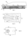
- Figure 1
- shows a cross-section view of an electronic module in which a chip carrier according to the invention can be used.
- Figure 2
- comprising
Figures 2a ,2b and2c , depicts a particular chip carrier according to the inven- tion.Figures 2a and2b illustrate in plan view and in cross-section, respectively, whileFigure 2c is a plan view of a specific conductive layer. - Figure 3
- comprising 3a and 3b, is an eye-diagram of a signal in a known electronic device and in an electronic device including the chip carrier according to the invention, respectively.
- Figure 4
- comprising 4a and 4b, shows the same signals in the frequency domain.
- For sake of illustration, the following description is based on Ball Grid Array (BGA) package wherein chip to chip carrier interconnection is performed with Controlled Collapse Chip Connection (IBM C4 technology), widely known as Flip-Chip Attach (FCA). Such technology provides high I/O density, uniform chip power distribution, high cooling capability and high reliability.
- With reference in particular to
Figure 1 , there is depicted anelectronic module 100 of the BGA type. Theelectronic module 100 includes achip 105 of semiconductor material, wherein a power circuit working at a high frequency, e.g. with a clock rate of 5 GHz, is integrated.Chip 105, supplied by a low voltage power supply, e.g. 1.2V., is mounted on alaminate chip carrier 110 comprising several conductive layers, e.g. made of copper, insulated from each other by means of a dielectric material, e.g. Polytetraflouroethylene (PTFE).Chip 105 tochip carrier 110 interconnection is performed withC4 balls 115 whilechip carrier 110 to printed circuit board (not represented) interconnection is done withBGA balls 120.Chip carrier 110 is glued tostiffener 125 that comprises cavities forchip 105 and, optionally, other electronic components such ascapacitor 130. Stiffener 125 consists preferably of a metallic plate, e.g. made of copper, which increases the rigidity of the entireelectronic module 100 and provides further path to dissipate thermal energy produced bychip 105.Chip 105 andstiffener 125 are covered bylid 135, e.g. made of copper, which also acts as a heat-spreader for dissipating the heat produced bychip 105 as well as providing mechanical protection forchip 105.Layers 140 comprise glue, e.g. epoxy glue, that fixed togetherchip carrier 110,chip 105,stiffener 125 andlid 135. Glue also compensates for the different coefficients of thermal expansion ofchip carrier 110,chip 105,stiffener 125 andlid 135. - Likewise considerations apply if the electronic device is not of the BGA type, if the chip does not embody a (digital) power circuit, if it works at a different frequency or with a different power supply, and so on.
- Considering now
Figure 2a illustrating a partial plan view ofchip carrier 110, there is shown a track, referred to as 200, ending with apad 205, which may be connected to interconnectingball 210, with a through via, which is used for transmitting a high-frequency signal. A couple of coplanar tracks, referred to as 215a and 215b respectively, are arranged aroundsignal track 200 and may be formed in the same conductive layer as illustrated. Coplanartracks 215a and 215b end withpad 220 for interconnectingball 225 which is linked totrack 230, formed in another conductive layer, and to a reference voltage or ground track formed in printed circuit board (not represented).Track 230 is partially superimposed to track 200 andcoplanar tracks 215a and 215b. - The high-frequency signal transmitted on
track 200 generates an electromagnetic wave which propagates along a transmission line defined bysignal track 200,coplanar tracks 215a and 215b andtrack 230. - Considering now the cross-section along line A-A, as shown on
Figure 2b ,chip carrier 110 is insulated from chip 105 (not represented) and printed circuit board (not represented) by means of insulatingfilms 235 and 235', respectively. Insulatingfilms 235 and 235' comprise openings wherein pads,e.g. pad 205, are formed.Chip carrier 110 comprises severalconductive layers 240a to 240g (seven in the example at issue), that are insulated from each other by means of adielectric material 245, e.g. PTFE.Conductive layers 240a to 240g provide electrical connection betweenchip 105 and the printed circuit board (not represented) on whichelectronic module 100 is soldered. Generally speaking, design of tracks inconductive layers 240a to 240g is optimized so as to reduce cross-talk between signals and transmission delays. As a consequence,conductive layers conductive layers conductive layers conductive layers 240b to 240f and thus are used to form either (high frequency) signal tracks or reference voltage or ground tracks. - Thus, as an illustration,
signal track 200 andcoplanar tracks 215a and 215b are formed in the firstconductive layer 240a (starting from the lower surface of the chip carrier 110) andtrack 230 is formed in the secondconductive layer 240b (adjacent to the first conductive layer). - A via-
hole 250 connects the reference voltage or ground plane formed inconductive layer 240d to track 230 andcoplanar tracks 215a and 215b, and then to interconnectingball 225. - The reference voltage or ground planes formed in
conductive layer 240d,track 230 andcoplanar tracks 215a and 215b define a reference structure which controls the impedance of a transmission line associated with thesignal track 200 and shields thesignal track 200 from electromagnetic interference. - Proximity of conductive layers produces stray capacitors. In particular, stray capacitors are formed between interconnecting
balls ball 210 and tracks formed inconductive layer 240b. - The inventors have discovered that the degradation of the performance of the known electronic devices is mainly due to a discontinuity in the transmission line associated with the interconnecting
ball 210. The transmission line is actually subjected to a sharp change of direction, from an horizontal direction along thesignal track 200 to a vertical direction going up to the interconnectingball 210. Particularly, the stray capacitor formed between interconnectingball 210 and tracks formed inconductive layer 240b has a relative high capacitance if compared to the one formed between interconnectingballs ball 210 and tracks formed inconductive layer 240b may be reduced by implementing openings inconductive layers e.g. pad 205, i.e. by excluding any signal or reference voltage tracks. However, these openings may lead to manufacturing drawbacks, e.g. flatness ofchip carrier 110, since conductive layer thickness, e.g. 12µm, of package structure can not be disregarded when considering dielectric layer thickness, e.g. 35µm. It becomes evident how difficult could be to replenish the large areas created by removing conductive material, e.g. 600 to 800µm in diameter, inlayer 240b, to maintain flatness across the whole package surface area. A further manufacturing drawback is the extended dielectric material to dielectric material interface that is a very critical adhesion interface for such large areas. Thus, the invention is going in the opposite direction of aforementioned approach, it consists in implementing annular ring openings, e.g. 255, wherein central floating disks, e.g. 260, made of conductive material, that are not connected to any signal, reference voltage or ground planes, as illustrated onFigures 2b and2c . -
Shape 265 represents the location in which no signal, reference voltage or ground plane has to be formed so as to reduce low pass filter effects mentioned above.Shape 265 is formed by superposing conical and cylindrical parts having a common axis, perpendicular toconductive layer 240a. A first cylindrical part is delimited by first and secondconductive layers conductive layers conductive layer 240c wherein signal tracks are formed and the closestconductive layer 240d wherein further reference voltage or ground tracks are formed. The smaller diameter of conical part corresponds to the diameter of first cylindrical part and the diameter of the second cylindrical part corresponds to the greater diameter of the conical part, as illustrated. Diameter of first cylindrical part is determined by contact area corresponding to pad 205, its value is at least equal to orthographic projection of this contact area corresponding to pad 205. Conical part angle is comprised between 30° and 60° and is preferably equal to 45°, as shown. A floatingdisk 260, made of conductive material, is formed inconductive layer 240b to createannular ring 255, made of insulating material, betweenreference plane 230 and floatingdisk 260 as illustrated onFigures 2b and2c . In a preferred embodiment, cross-section ofannular ring 255 is centred on orthographic projection of contact area corresponding to pad 205. Floatingdisk 260 is not connected to any signal, reference voltage or ground track. For example, considering contact area corresponding to pad 205 having a diameter equal to 600µm, the diameter of the openings must be at least equal to 600µm however, a greater diameter improves signal shielding. Inventors have observed that, in such cases, opening diameter equals to 800µm and floating disk diameter equals to 600µm are values that provide an efficient signal shielding while optimizing dedicated surface area and physical parameters mentioned above, e.g. flatness across the whole package surface area and dielectric material to dielectric material adhesion. - Likewise considerations apply if the chip carrier has a different structure, for example with two differential signal tracks arranged between the coplanar tracks, if the chip carrier includes a different number of conductive layers, if a further ground plane is provided on top of the first layer wherein the signal tracks are formed, if the ground planes and the power plane consists each of two or more distinct tracks, if the contact area has a different dimension, and so on.
- More generally, the present invention provides an electronic device carrier for transmitting high-frequency signals, including a circuitised substrate with a plurality of conductive layers insulated from each other ; the conductive layers are arranged in a sequence from a first one of the conductive layers wherein a plurality of signal tracks are formed, each one ending with a contact area for transmitting a high-frequency signal. The electronic device carrier further includes a reference structure connectable to a reference voltage or ground for shielding the signal tracks ; the reference structure has at least one reference track formed in a second one of the conductive layers adjacent to the first conductive layer and at least one further reference track formed in one of the conductive layers different from the first and second conductive layer ; a portion of each signal track excluding at least the area corresponding to the orthographic projection of associated contact area, i.e. pad, is superimposed in plan view to a corresponding reference track, and at least a part of the area corresponding to the orthographic projection of contact area, i.e. pad, associated to each signal track, is superimposed in plan view to a corresponding further reference track with interposition of a floating conductive track not connected to any signal, reference voltage or ground track.
- The devised solution strongly reduces the capacitance of the stray capacitor formed between the signal track and the reference plane in the area of the interconnecting ball (being inversely proportional to their distance).
- The solution of the invention maintains a good integrity of the electromagnetic wave propagated along the transmission line. The proposed design of the electronic device carrier affects the performance of the chip as little as possible, so that the whole electronic system can be operated at a frequency very close to the working frequency which is afforded by the chip.
- Moreover, the solution according to the invention maintains the bandwidth of the transmission line at a satisfactory value, even if the dimensions of the signal track (and then also the width of the dielectric layer between the signal track and the adjacent reference plane) are reduced. Therefore, this structure makes it possible to produce electronic system of very small dimensions, but at the same time with a high performance.
- Considering manufacturing and mechanical aspects, the solution of the invention is adapted for flatness electronic device carrier for transmitting high frequency signals and allows to match coefficient expansion between electronic device carrier, electronic device and electronic system on which it is connected since contact areas of adjacent dielectric material layers are minimized with an improved adhesion between layers in the electronic device carrier multilayer structure.
- With reference in particular to
Figure 3a , there is depicted an eye-diagram for a known electronic module, with a single reference plane adjacent to the signal track, which also overlaps the respective interconnecting ball. This diagram shows the value (in V) of a signal s(t) received from a transmission line as a function of the phase of a clock signal ; the eye-diagram is quite close, due to the discontinuities in the transmission line. Conversely, an eye-diagram for the electronic module embedding the chip carrier of the invention, as shown inFigure 3b , is more open, so that it is easier to discriminate an actual switching transition of the signal from a shift of a signal baseline due to a background noise. As a consequence, the electronic module can be operated at a high-frequency even with a reduced level of the power supply voltage. - In other words, in the known electronic module the low-pass filter defined by the stray capacitor formed between the pad and the underlying reference plane has a very low cut-off frequency ; therefore, as shown in
Figure 4a , only the first harmonic f0 of the signal s(f) (expressed in the frequency domain) is hardly transmitted. On the other hand, the solution of the invention increases the bandwidth of the transmission line up to the third harmonic 3f0 of the signal, as shown inFigure 4b . - While the invention has been described by reference to chip carriers for transmitting high frequency signals from the chip carrier to a printed circuit board, the invention may be efficiently applied in the chip carrier to reduce effects of discontinuity in the transmission lines close to C4 pad or pad used for wire bonded connection.
- Stray capacitor effects in printed circuit boards are generally negligible since the ratio of dielectric layer thickness between signal, reference voltage and ground tracks and track width is often great enough. Thus, there is generally no need to implement the invention in printed circuit boards, even if it could be done without drawback, except regarding costs. However, due to miniaturization trend, the above mentioned low pass filter effects of the chip carrier may arise in printed circuit boards, e.g. in teflon based printed circuit boards. In such cases, stray capacitor effects may be reduced by implementing the invention in the printed circuit board itself.
- Naturally, in order to satisfy local and specific requirements, a person skilled in the art may apply to the solution described above many modifications and alterations all of which, however, are included within the scope of protection of the invention as defined by the following claims.
Claims (11)
- An electronic device carrier (110) adapted for transmitting high-frequency signals, comprising: a circuitized substrate with a plurality of conductive layers (240a-g) insulated from each other, the conductive layers being arranged in sequence from a first conductive layer (240a) at a first major surface of the substrate, the first conductive layer comprising a signal track (200) ending with a contact area (205) for transmitting a high-frequency signal; a reference structure (215a, 215b, 230) connectable to a reference voltage or ground for shielding the signal track,
the reference structure including at least one reference track (230) formed in a second conductive layer (240b) adjacent to the first conductive layer and at least one further reference track formed in a third conductive layer (240d) different from the first and second conductive layers;
a fourth conductive layer (240c), adapted for transmitting a high frequency signal, located between said second and third conductive layers;
each of said second (240b), and fourth (240c) conductive layers comprising an opening (255, 265) at a portion of the respective conductive layer corresponding to the location of the orthographic projection of the contact area (205) of said first conductive layer from which any signal, ground plane, or reference voltage tracks are excluded;
characterized in that
an electrically floating disk (260), made of conductive material and not connected to any signal, reference voltage or ground plane, is formed in said opening of said second conductive layer (240b). - The electronic device carrier (110) according to claim 1, wherein said fourth conductive layer (240c) comprises a plurality of signal tracks and the openings in said second and fourth conductive layers (240b,c) define a conical shadow area defined by a smaller diameter end corresponding to the opening in the second conductive layer (240b) and larger diameter end corresponding to the opening in the fourth conductive layer (240c) the surface of said conical shadow area that intersects the second and fourth conductive layers (240b,c) forming an angle in the range between 30° and 60° with the second and fourth conductive layers (240b,c).
- The electronic device carrier (110) according to claim 2, wherein said angle is 45°.
- The electronic device carrier (110) according to claims 1, to 3, wherein the reference structure (215a, 215b, 230) further includes a plurality of couples of coplanar tracks (215a, 215b) formed in the first conductive layer (240a), each signal track (200) being arranged between the coplanar tracks of a corresponding couple.
- The electronic device carrier (110) according to claim 4, further including a plurality of via-holes (250) each one connecting a coplanar track (215a) to the corresponding reference track (230) and to the corresponding further reference track.
- The electronic device carrier of claims 1 to 5 wherein a chip (105) is mounted thereon.
- The electronic device carrier (110) according to claim 6, further including a plurality of interconnecting balls (210, 225) each one arranged on a corresponding contact area (205, 220).
- A high-frequency electronic device (100) including the electronic device carrier (110) according to claims 1 to 7, a chip of semiconductor material (105) with a plurality of terminals, the chip being mounted on the carrier, and means for electrically connecting each terminal of the chip to a corresponding contact area (205).
- The electronic device (100) according to claim 8, wherein terminals of the chip (105) are connected to the corresponding contact areas by means of interconnecting balls (115).
- The electronic device (100) according to claim 8, wherein terminals of the chip (105) are wire bonded to the corresponding contact areas.
- The electronic device carrier of claims 1 to 5 wherein said device carrier is a printed circuit board.
Priority Applications (1)
| Application Number | Priority Date | Filing Date | Title |
|---|---|---|---|
| EP02795072A EP1444733B1 (en) | 2001-11-13 | 2002-10-25 | Electronic device carrier adapted for transmitting high frequency signals |
Applications Claiming Priority (4)
| Application Number | Priority Date | Filing Date | Title |
|---|---|---|---|
| EP01480110 | 2001-11-13 | ||
| EP01480110 | 2001-11-13 | ||
| PCT/EP2002/013209 WO2003043085A2 (en) | 2001-11-13 | 2002-10-25 | Electronic device carrier adapted for transmitting high frequency signals |
| EP02795072A EP1444733B1 (en) | 2001-11-13 | 2002-10-25 | Electronic device carrier adapted for transmitting high frequency signals |
Publications (2)
| Publication Number | Publication Date |
|---|---|
| EP1444733A2 EP1444733A2 (en) | 2004-08-11 |
| EP1444733B1 true EP1444733B1 (en) | 2010-12-01 |
Family
ID=8183420
Family Applications (1)
| Application Number | Title | Priority Date | Filing Date |
|---|---|---|---|
| EP02795072A Expired - Lifetime EP1444733B1 (en) | 2001-11-13 | 2002-10-25 | Electronic device carrier adapted for transmitting high frequency signals |
Country Status (9)
| Country | Link |
|---|---|
| US (1) | US7015574B2 (en) |
| EP (1) | EP1444733B1 (en) |
| JP (1) | JP4222943B2 (en) |
| KR (1) | KR100613820B1 (en) |
| CN (1) | CN1314114C (en) |
| AT (1) | ATE490554T1 (en) |
| AU (1) | AU2002360943A1 (en) |
| DE (1) | DE60238501D1 (en) |
| WO (1) | WO2003043085A2 (en) |
Cited By (1)
| Publication number | Priority date | Publication date | Assignee | Title |
|---|---|---|---|---|
| CN109564263A (en) * | 2016-08-17 | 2019-04-02 | 通用电气航空系统有限公司 | Method and apparatus for detecting the electric fault in printed circuit board |
Families Citing this family (12)
| Publication number | Priority date | Publication date | Assignee | Title |
|---|---|---|---|---|
| JP3580803B2 (en) * | 2002-08-09 | 2004-10-27 | 沖電気工業株式会社 | Semiconductor device |
| JP2004214657A (en) | 2003-01-07 | 2004-07-29 | Internatl Business Mach Corp <Ibm> | Water-soluble protective paste for printed circuit board manufacturing |
| JP4957013B2 (en) * | 2006-02-24 | 2012-06-20 | 凸版印刷株式会社 | Semiconductor device mounting substrate |
| US20070200234A1 (en) * | 2006-02-28 | 2007-08-30 | Texas Instruments Incorporated | Flip-Chip Device Having Underfill in Controlled Gap |
| US20080093726A1 (en) * | 2006-10-23 | 2008-04-24 | Francesco Preda | Continuously Referencing Signals over Multiple Layers in Laminate Packages |
| EP2493273A4 (en) * | 2009-10-23 | 2013-10-16 | Fujikura Ltd | STRUCTURE AND METHOD FOR MOUNTING DEVICE |
| US8325459B2 (en) * | 2009-12-08 | 2012-12-04 | International Business Machines Corporation | Channel performance of electrical lines |
| US8890302B2 (en) * | 2012-06-29 | 2014-11-18 | Intel Corporation | Hybrid package transmission line circuits |
| US9373600B2 (en) * | 2014-01-27 | 2016-06-21 | Semiconductor Components Industries, Llc | Package substrate structure for enhanced signal transmission and method |
| KR20200100967A (en) | 2019-02-19 | 2020-08-27 | 주식회사 엘지화학 | Integrated circuit chip and circuit system using the same |
| KR20200145589A (en) | 2019-06-22 | 2020-12-30 | 김민태 | Lens cleaner, can augment functions in sterilization |
| JP2024153955A (en) * | 2021-07-13 | 2024-10-30 | 株式会社村田製作所 | Circuit boards and electronic components |
Family Cites Families (7)
| Publication number | Priority date | Publication date | Assignee | Title |
|---|---|---|---|---|
| JPS6260773A (en) * | 1985-09-09 | 1987-03-17 | Howa Mach Ltd | Bobbin down conveying device |
| DE4100238A1 (en) * | 1991-01-07 | 1992-07-09 | Philips Patentverwaltung | VIELLAGE BOARD, ESPECIALLY FOR HIGH FREQUENCY |
| JPH06260773A (en) * | 1993-03-03 | 1994-09-16 | Oki Electric Ind Co Ltd | Pad structure of high speed signal transmission circuit board |
| US5338970A (en) | 1993-03-24 | 1994-08-16 | Intergraph Corporation | Multi-layered integrated circuit package with improved high frequency performance |
| US5691568A (en) * | 1996-05-31 | 1997-11-25 | Lsi Logic Corporation | Wire bondable package design with maxium electrical performance and minimum number of layers |
| US5907265A (en) * | 1996-09-13 | 1999-05-25 | Matsushita Electric Industrial Co., Ltd. | High-frequency circuit board trace crossing and electronic component therefor |
| JPH118445A (en) * | 1997-06-18 | 1999-01-12 | Toyota Motor Corp | Circuit board |
-
2002
- 2002-10-25 CN CNB028201981A patent/CN1314114C/en not_active Expired - Fee Related
- 2002-10-25 EP EP02795072A patent/EP1444733B1/en not_active Expired - Lifetime
- 2002-10-25 JP JP2003544815A patent/JP4222943B2/en not_active Expired - Fee Related
- 2002-10-25 WO PCT/EP2002/013209 patent/WO2003043085A2/en not_active Ceased
- 2002-10-25 AU AU2002360943A patent/AU2002360943A1/en not_active Abandoned
- 2002-10-25 KR KR1020047001388A patent/KR100613820B1/en not_active Expired - Fee Related
- 2002-10-25 AT AT02795072T patent/ATE490554T1/en not_active IP Right Cessation
- 2002-10-25 US US10/495,674 patent/US7015574B2/en not_active Expired - Fee Related
- 2002-10-25 DE DE60238501T patent/DE60238501D1/en not_active Expired - Lifetime
Cited By (2)
| Publication number | Priority date | Publication date | Assignee | Title |
|---|---|---|---|---|
| CN109564263A (en) * | 2016-08-17 | 2019-04-02 | 通用电气航空系统有限公司 | Method and apparatus for detecting the electric fault in printed circuit board |
| CN109564263B (en) * | 2016-08-17 | 2021-08-10 | 通用电气航空系统有限公司 | Method and apparatus for detecting electrical faults in printed circuit boards |
Also Published As
| Publication number | Publication date |
|---|---|
| KR20040044437A (en) | 2004-05-28 |
| KR100613820B1 (en) | 2006-08-21 |
| EP1444733A2 (en) | 2004-08-11 |
| JP2005533366A (en) | 2005-11-04 |
| ATE490554T1 (en) | 2010-12-15 |
| WO2003043085A2 (en) | 2003-05-22 |
| CN1568545A (en) | 2005-01-19 |
| DE60238501D1 (en) | 2011-01-13 |
| JP4222943B2 (en) | 2009-02-12 |
| US20050006137A1 (en) | 2005-01-13 |
| WO2003043085A3 (en) | 2003-11-06 |
| US7015574B2 (en) | 2006-03-21 |
| AU2002360943A1 (en) | 2003-05-26 |
| CN1314114C (en) | 2007-05-02 |
Similar Documents
| Publication | Publication Date | Title |
|---|---|---|
| CN100370887C (en) | Improved stacked via structure in a multi-layer electronic device carrier | |
| US6710258B2 (en) | Circuitized substrate for high-frequency applications | |
| JP4404252B2 (en) | Printed circuit board having high speed performance and manufacturing method thereof | |
| US7015574B2 (en) | Electronic device carrier adapted for transmitting high frequency signals | |
| CA2454971A1 (en) | Multi-chip electronic package having laminate carrier and method of making same | |
| CN101095380A (en) | Multilayer printed circuit boards including through connections for high frequency applications | |
| US7388158B2 (en) | Concentric spacer for reducing capacitive coupling in multilayer substrate assemblies | |
| EP1085594B1 (en) | High frequency circuit apparatus | |
| TW201740487A (en) | Integrated circuit package device provided with antenna and manufacturing method thereof | |
| US20050191785A1 (en) | Via structure of packages for high frequency semiconductor devices | |
| US6717255B2 (en) | Chip carrier for a high-frequency electronic package | |
| JP2002252298A (en) | Wiring board and semiconductor device using the same | |
| TWI804335B (en) | Circuit board structure | |
| JP2001203300A (en) | Wiring substrate, semiconductor device, and method of manufacturing wiring substrate | |
| JP4616968B2 (en) | High frequency semiconductor device using interposer | |
| JP2008159752A (en) | Semiconductor device | |
| JP2004241426A (en) | Wiring board | |
| JP2006269627A (en) | Via structure for printed wiring board | |
| WO2006019336A2 (en) | Impedance controlled interconnect substrate and package for high-frequency electronic device | |
| JPH0432252A (en) | Electronic component mounting board | |
| JP2005244110A (en) | Multilayer substrate and high-frequency circuit device | |
| JP2004031530A (en) | Integrated circuit device | |
| JP2001102488A (en) | Semiconductor device | |
| JPH03283592A (en) | Multilayer circuit board | |
| JP2007258762A (en) | Multilayer board |
Legal Events
| Date | Code | Title | Description |
|---|---|---|---|
| PUAI | Public reference made under article 153(3) epc to a published international application that has entered the european phase |
Free format text: ORIGINAL CODE: 0009012 |
|
| 17P | Request for examination filed |
Effective date: 20040312 |
|
| AK | Designated contracting states |
Kind code of ref document: A2 Designated state(s): AT BE BG CH CY CZ DE DK EE ES FI FR GB GR IE IT LI LU MC NL PT SE SK TR |
|
| AX | Request for extension of the european patent |
Extension state: AL LT LV MK RO SI |
|
| 17Q | First examination report despatched |
Effective date: 20080403 |
|
| RAP1 | Party data changed (applicant data changed or rights of an application transferred) |
Owner name: INTERNATIONAL BUSINESS MACHINES CORPORATION |
|
| RBV | Designated contracting states (corrected) |
Designated state(s): AT BE BG CH CY CZ DE DK EE ES FI FR GB GR IE IT LI LU NL PT SE SK TR |
|
| GRAP | Despatch of communication of intention to grant a patent |
Free format text: ORIGINAL CODE: EPIDOSNIGR1 |
|
| GRAS | Grant fee paid |
Free format text: ORIGINAL CODE: EPIDOSNIGR3 |
|
| GRAA | (expected) grant |
Free format text: ORIGINAL CODE: 0009210 |
|
| AK | Designated contracting states |
Kind code of ref document: B1 Designated state(s): AT BE BG CH CY CZ DE DK EE ES FI FR GB GR IE IT LI LU NL PT SE SK TR |
|
| REG | Reference to a national code |
Ref country code: GB Ref legal event code: FG4D |
|
| REG | Reference to a national code |
Ref country code: CH Ref legal event code: EP |
|
| REG | Reference to a national code |
Ref country code: IE Ref legal event code: FG4D Ref country code: GB Ref legal event code: 746 Effective date: 20101215 |
|
| REF | Corresponds to: |
Ref document number: 60238501 Country of ref document: DE Date of ref document: 20110113 Kind code of ref document: P |
|
| REG | Reference to a national code |
Ref country code: NL Ref legal event code: VDEP Effective date: 20101201 |
|
| PG25 | Lapsed in a contracting state [announced via postgrant information from national office to epo] |
Ref country code: FI Free format text: LAPSE BECAUSE OF FAILURE TO SUBMIT A TRANSLATION OF THE DESCRIPTION OR TO PAY THE FEE WITHIN THE PRESCRIBED TIME-LIMIT Effective date: 20101201 Ref country code: AT Free format text: LAPSE BECAUSE OF FAILURE TO SUBMIT A TRANSLATION OF THE DESCRIPTION OR TO PAY THE FEE WITHIN THE PRESCRIBED TIME-LIMIT Effective date: 20101201 Ref country code: BG Free format text: LAPSE BECAUSE OF FAILURE TO SUBMIT A TRANSLATION OF THE DESCRIPTION OR TO PAY THE FEE WITHIN THE PRESCRIBED TIME-LIMIT Effective date: 20110301 Ref country code: NL Free format text: LAPSE BECAUSE OF FAILURE TO SUBMIT A TRANSLATION OF THE DESCRIPTION OR TO PAY THE FEE WITHIN THE PRESCRIBED TIME-LIMIT Effective date: 20101201 Ref country code: CY Free format text: LAPSE BECAUSE OF FAILURE TO SUBMIT A TRANSLATION OF THE DESCRIPTION OR TO PAY THE FEE WITHIN THE PRESCRIBED TIME-LIMIT Effective date: 20101201 Ref country code: SE Free format text: LAPSE BECAUSE OF FAILURE TO SUBMIT A TRANSLATION OF THE DESCRIPTION OR TO PAY THE FEE WITHIN THE PRESCRIBED TIME-LIMIT Effective date: 20101201 |
|
| PG25 | Lapsed in a contracting state [announced via postgrant information from national office to epo] |
Ref country code: GR Free format text: LAPSE BECAUSE OF FAILURE TO SUBMIT A TRANSLATION OF THE DESCRIPTION OR TO PAY THE FEE WITHIN THE PRESCRIBED TIME-LIMIT Effective date: 20110302 |
|
| PG25 | Lapsed in a contracting state [announced via postgrant information from national office to epo] |
Ref country code: ES Free format text: LAPSE BECAUSE OF FAILURE TO SUBMIT A TRANSLATION OF THE DESCRIPTION OR TO PAY THE FEE WITHIN THE PRESCRIBED TIME-LIMIT Effective date: 20110312 Ref country code: BE Free format text: LAPSE BECAUSE OF FAILURE TO SUBMIT A TRANSLATION OF THE DESCRIPTION OR TO PAY THE FEE WITHIN THE PRESCRIBED TIME-LIMIT Effective date: 20101201 Ref country code: EE Free format text: LAPSE BECAUSE OF FAILURE TO SUBMIT A TRANSLATION OF THE DESCRIPTION OR TO PAY THE FEE WITHIN THE PRESCRIBED TIME-LIMIT Effective date: 20101201 Ref country code: CZ Free format text: LAPSE BECAUSE OF FAILURE TO SUBMIT A TRANSLATION OF THE DESCRIPTION OR TO PAY THE FEE WITHIN THE PRESCRIBED TIME-LIMIT Effective date: 20101201 Ref country code: PT Free format text: LAPSE BECAUSE OF FAILURE TO SUBMIT A TRANSLATION OF THE DESCRIPTION OR TO PAY THE FEE WITHIN THE PRESCRIBED TIME-LIMIT Effective date: 20110401 |
|
| PG25 | Lapsed in a contracting state [announced via postgrant information from national office to epo] |
Ref country code: SK Free format text: LAPSE BECAUSE OF FAILURE TO SUBMIT A TRANSLATION OF THE DESCRIPTION OR TO PAY THE FEE WITHIN THE PRESCRIBED TIME-LIMIT Effective date: 20101201 |
|
| PLBE | No opposition filed within time limit |
Free format text: ORIGINAL CODE: 0009261 |
|
| STAA | Information on the status of an ep patent application or granted ep patent |
Free format text: STATUS: NO OPPOSITION FILED WITHIN TIME LIMIT |
|
| PG25 | Lapsed in a contracting state [announced via postgrant information from national office to epo] |
Ref country code: DK Free format text: LAPSE BECAUSE OF FAILURE TO SUBMIT A TRANSLATION OF THE DESCRIPTION OR TO PAY THE FEE WITHIN THE PRESCRIBED TIME-LIMIT Effective date: 20101201 |
|
| 26N | No opposition filed |
Effective date: 20110902 |
|
| REG | Reference to a national code |
Ref country code: DE Ref legal event code: R097 Ref document number: 60238501 Country of ref document: DE Effective date: 20110902 |
|
| PG25 | Lapsed in a contracting state [announced via postgrant information from national office to epo] |
Ref country code: IT Free format text: LAPSE BECAUSE OF FAILURE TO SUBMIT A TRANSLATION OF THE DESCRIPTION OR TO PAY THE FEE WITHIN THE PRESCRIBED TIME-LIMIT Effective date: 20101201 |
|
| REG | Reference to a national code |
Ref country code: CH Ref legal event code: PL |
|
| REG | Reference to a national code |
Ref country code: FR Ref legal event code: ST Effective date: 20120629 |
|
| PG25 | Lapsed in a contracting state [announced via postgrant information from national office to epo] |
Ref country code: LI Free format text: LAPSE BECAUSE OF NON-PAYMENT OF DUE FEES Effective date: 20111031 Ref country code: CH Free format text: LAPSE BECAUSE OF NON-PAYMENT OF DUE FEES Effective date: 20111031 |
|
| REG | Reference to a national code |
Ref country code: IE Ref legal event code: MM4A |
|
| PG25 | Lapsed in a contracting state [announced via postgrant information from national office to epo] |
Ref country code: FR Free format text: LAPSE BECAUSE OF NON-PAYMENT OF DUE FEES Effective date: 20111102 |
|
| PG25 | Lapsed in a contracting state [announced via postgrant information from national office to epo] |
Ref country code: IE Free format text: LAPSE BECAUSE OF NON-PAYMENT OF DUE FEES Effective date: 20111025 |
|
| PG25 | Lapsed in a contracting state [announced via postgrant information from national office to epo] |
Ref country code: LU Free format text: LAPSE BECAUSE OF NON-PAYMENT OF DUE FEES Effective date: 20111025 |
|
| PG25 | Lapsed in a contracting state [announced via postgrant information from national office to epo] |
Ref country code: TR Free format text: LAPSE BECAUSE OF FAILURE TO SUBMIT A TRANSLATION OF THE DESCRIPTION OR TO PAY THE FEE WITHIN THE PRESCRIBED TIME-LIMIT Effective date: 20101201 |
|
| PGFP | Annual fee paid to national office [announced via postgrant information from national office to epo] |
Ref country code: DE Payment date: 20181121 Year of fee payment: 17 |
|
| PGFP | Annual fee paid to national office [announced via postgrant information from national office to epo] |
Ref country code: GB Payment date: 20181025 Year of fee payment: 17 |
|
| REG | Reference to a national code |
Ref country code: DE Ref legal event code: R119 Ref document number: 60238501 Country of ref document: DE |
|
| PG25 | Lapsed in a contracting state [announced via postgrant information from national office to epo] |
Ref country code: DE Free format text: LAPSE BECAUSE OF NON-PAYMENT OF DUE FEES Effective date: 20200501 |
|
| GBPC | Gb: european patent ceased through non-payment of renewal fee |
Effective date: 20191025 |
|
| PG25 | Lapsed in a contracting state [announced via postgrant information from national office to epo] |
Ref country code: GB Free format text: LAPSE BECAUSE OF NON-PAYMENT OF DUE FEES Effective date: 20191025 |