EP1443542A2 - Verfahren und Vorrichtung zum Kontrollieren des Randes eines scheibenförmigen Gegenstandes - Google Patents
Verfahren und Vorrichtung zum Kontrollieren des Randes eines scheibenförmigen Gegenstandes Download PDFInfo
- Publication number
- EP1443542A2 EP1443542A2 EP04001554A EP04001554A EP1443542A2 EP 1443542 A2 EP1443542 A2 EP 1443542A2 EP 04001554 A EP04001554 A EP 04001554A EP 04001554 A EP04001554 A EP 04001554A EP 1443542 A2 EP1443542 A2 EP 1443542A2
- Authority
- EP
- European Patent Office
- Prior art keywords
- edge
- wafer
- sensor
- gripper
- inspection
- Prior art date
- Legal status (The legal status is an assumption and is not a legal conclusion. Google has not performed a legal analysis and makes no representation as to the accuracy of the status listed.)
- Granted
Links
Images


Classifications
-
- H10P72/53—
-
- G—PHYSICS
- G01—MEASURING; TESTING
- G01N—INVESTIGATING OR ANALYSING MATERIALS BY DETERMINING THEIR CHEMICAL OR PHYSICAL PROPERTIES
- G01N21/00—Investigating or analysing materials by the use of optical means, i.e. using sub-millimetre waves, infrared, visible or ultraviolet light
- G01N21/84—Systems specially adapted for particular applications
- G01N21/88—Investigating the presence of flaws or contamination
- G01N21/95—Investigating the presence of flaws or contamination characterised by the material or shape of the object to be examined
- G01N21/9501—Semiconductor wafers
- G01N21/9503—Wafer edge inspection
-
- H10P72/0616—
-
- H10P72/7602—
Definitions
- the invention relates to a method and an apparatus for Checking the edge of disc-shaped objects, in particular essentially circular and / or thin Disks, such as semiconductor wafers.
- Thin wafers are wafers that are already at least half of their original Thickness has been thinned.
- the edge should preferably checked both on the front and on the back to make appropriate statements for process control to deliver.
- Edge inspection of wafers especially of Thin wafers or thin wafers mounted on carrier wafers only through an optical control with the help of a Microscope executed. Doing so at a certain magnification the wafer edge optically checked, any edge damage classified, for example as microscopic Hairline crack, as a shell breakout or as similar damage, and entered into a card of the wafer by hand.
- the map is also known as a wafer map. This The process is extremely time-consuming and subjective, so the Classification of marginal damage or marginal defects only based on subjective impressions of the The examining person is carried out.
- the invention is based on the object, a method and to specify a device of the type mentioned at the outset, with the edge of a disc-shaped object, such as a wafer, even if it's a thin slice, e.g. a thin wafer or around one on a carrier wafer assembled thin wafers, completely or largely can be executed automatically.
- this object is achieved with a method this is the characteristics of the method of the main claim having.
- Preferred and advantageous embodiments of the invention Device are the subject of the main device claim dependent subclaims.
- the edge of the Object e.g. a wafer with a width of about 2 mm (millimeters) examined for errors or damage.
- the type and size of the Errors determined, for example in a qualitative measurement and in a quantitative measurement. That through image processing Detected errors can be standardized using a classification to be expelled.
- the type and location of the error or the Save damage to the object or wafer in a file This allows a history of marginal damage to record over several process steps.
- special evaluation software can be provided, which provides the required functions.
- a special optic is provided to cover both the front and also the back of the edge of the wafer with a single one Record the camera at the same time
- the device according to the invention can be used consistently for the Handling thin slices, such as thin ones Wafers.
- a gripper can be provided for this be according to the Bernoulli principle in combination with negative pressure workable openings.
- the Bernoulli / vacuum gripper is briefly referred to below as a B / V gripper.
- a forced transfer from the B / V gripper to an inspection body or inspection jewelry and a thin-wafer-compatible tray mapping can be provided.
- the inspection jewelry disc-shaped objects of different sizes for example both 6-inch and 8-inch wafers for which Edge control can record and turn.
- a laser sensor is also provided, which is the location of the edge of the object, e.g. the wafer edge detected, and the deviation of the center of the wafer from the Center of the carrier determined and - if desired - the Position of the "flat”, i.e. a flattening at the edge of the wafer, or the "notch", i.e. a notch on the edge of wafers with more than 200mm diameter.
- the edge of the wafer is on a Sled mounted. This allows a follow-up arrangement the optics of the "eccentrically" running wafer edge to track. It is advantageous that the wafer is not must be centered on the inspection chuck, and that the Edge can also be checked automatically with the wafer flat can.
- the invention is basically any disc-shaped Objects applicable and not to a specific one Size of the object or wafer limited. Hence the in the following description of the drawings Reference to semiconductor wafers only for reference to FIG to understand preferred example.
- a robot 1 is provided in the arrangement shown in FIG. 1, whose arm 2 with one for handling thin wafers 10 equipped grippers 4 is equipped.
- This Gripper 4 can optionally be an input tray 6 and one Output Horde 8 can be assigned.
- the entrance horde is 6 also assigned a station 12 for "wafer mapping".
- An inspection piece 22 is located in an inspection station 20 provided to which a line sensor 24 is assigned. Furthermore is in the inspection station 20 using a Linear slide 26 linearly movable, optical sensor head 28 provided. In the inspection station 20 there is still a Bar code reader 30 arranged.
- FIG. 1 This arrangement shown in FIG. 1 is advantageous from the fact that it is suitable for thin wafers throughout.
- a wafer mapping sensor On the entrance horde 6 and possibly also the exit horde 8 a wafer mapping sensor, not shown, is installed, which the presence and deflection of the wafers 10 in the Horde 6, 8 notes. continues with the help of the wafer mapping sensor determined whether a wafer 10 is far from a Horde 6, 8 is leading.
- the decentration and the location of the Flats 14 of the wafer 10 on the chuck 22 in the inspection station 20 are determined so that when inspecting the optical sensor head 28 automatically tracks the wafer edge can be.
- the inspection station 20 is in an oblique view represented schematically. You can see the exit horde 8 and the wafer gripper 4, and the bar code reader 30, and in the actual inspection station 20 the inspection jewelry 22 with the carriers 34, 36, the wafers from the thin wafer gripper 4 on robot 1.
- the Carriers 34 and 36 are, as mentioned at the beginning, alternative ramped up, wherein in Fig. 2, a 6-inch wafer 10 on the Chuck 22, 34 is arranged at inspection height.
- the Optical sensor head 28 is already in the area of the edge of the 6-inch wafers 10 arranged and aligned so that it is in the front and the back in one operation of the edge of the wafer 10 can accommodate.
- the Carrier 22 slowly at a speed of about 4 to 6 rpm (Revolutions per minute).
- the optical sensor head 28 To ensure that despite the mostly existing wafer eccentricity, i.e. the center of the wafer is not the focus of the carrier 22, the optical sensor head 28 always in The edge area of the wafer 10 remains, the optical sensor head 28 adjusted the wafer edge. For this purpose, previously won Data from the line sensor 24 used. Put the dates e.g. from angle data and associated wafer edge position data together.
- the optical sensor head 28 can be implemented as in FIG Fig. 3 shown as an example.
- Embodiments are a camera 40 and a CCD sensor (Charged Coupled Device) via an optical system 42, 44 images of the top and bottom simultaneously of the wafer edge 16 supplied.
- Light reflected from the wafer edge 16 is reflected by the beam splitters 50 and passes over a lens and mirror system 42, 44 to the CCD sensor of the Camera 40.
- optical paths are provided so that on a CCD sensor Camera 40 both sides of the wafer edge 16 are imaged.
- the images of the Camera 40 or recorded by the CCD sensor which is a line CCD sensor can be, and put together into a strip.
- This strip forms the basis for the further one Image processing.
- the bar code reader 30 reads the bar code of the wafer 10 and this from the thin wafer gripper 3 into the exit horde 8 inserted.
- the Barcode read before or during the inspection.
- the image processing algorithms are executed when the Instructions of a program in a data processing system executed and evaluate the recorded by the optical sensor 28 Image of the wafer edge 16 and save the results in folders that are processed with the help of evaluation software can be.
- the evaluation software enables the view the errors at edge 16 detected by optical sensor 28 of the wafer 10 both in tabular form and graphically in a so-called "wafer map".
- a selection of errors can also be viewed as a wafer map file.
- the evaluation software enables several performed after successive treatment steps Controls of the edge of the wafer and their results as it were to lay one above the other and so a wafer 10 over to control several treatment stages.
- the evaluation software allows several batches of different Compare wafers 10 with each other. So can be determined whether and if so which process stages are prone to errors are, i.e. give rise to errors in the wafer edge, and a Show quality risk in the production line.
- This wafer 10 removed from the input tray 6 is then as shown in FIG. 4.2, on the inspection chuck 22 stored.
- the corresponding subchuck first drives of the inspection chuck 22 and takes over the wafer 10 Vacuum transfer directly from the thin wafer gripper 4.
- the thin wafer gripper 4 releases the wafer 10 by releasing its vacuum free and then moves down and back.
- the right Chuck drives the support of the wafer 10 34, 36, e.g. the 200mm chuck 36, and clamps the wafer 10 also with vacuum. The edge of the wafer is still sticking out on all sides beyond the chuck 34 or 36.
- the line sensor 24 has advanced to scan the wafer edge 16, the Wafer 10 rotates once through 360 °. This will change the location of the Wafer edge 16 measured and from this the eccentricity of the wafer 10 calculated. If 6-inch wafer 10 in its edge area 16 are checked, the line sensor 24 also Flat 14 recorded, i.e. the flattened area on the peripheral edge of the wafer 10. The position data for the wafer edge 16, the have been detected by the line sensor 24 are in the inspection station 20 saved.
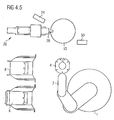
- Fig. 4.5 shows the situation in which the optical sensor 28 using its linear drive 26 in the the position 16 assigned to the edge 16 of the wafer has advanced. Due to the construction of the optical described above Sensors 28 become both the front and the back of wafer 10, i.e. the top side and the bottom side, in Edge area 16 examined.
- the edge area 16 has, for example Width of about 2 mm (millimeters). So far from wafer 10 - what will usually be the case - not centered on the carrier 22 lies, the previously saved and from the line sensor 24th captured position data used to the optical Sensor 28 with the help of its linear slide 26 so radially to Wafer 16 to adjust that he the edge 16 of the wafer 10 is always updated. If a 6-inch wafer 10 with flat 14 can be checked, it can be ensured that the edge 16 also in the area of the flat 14 by appropriate Moving the optical sensor 28 while rotating the wafer 10 is checked.
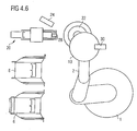
- Fig. 4.6 shows how the wafer checks after its edge has been corrected from subchuck 22 to the thin wafer gripper 4 is passed.
- the thin wafer gripper 4 grips the wafer 10 such that the Center of the wafer 10 exactly the desired location on the Thin wafer gripper 4 takes, where then usually the center of the wafer 4 coincides with the center of the thin wafer gripper 4.
- the one arranged on the wafer 10 Barcode read using the barcode reader 30, such as this is also shown in Fig. 4.6.
- the edge area of the wafer on both sides simultaneously, i.e. above and below, through an optical sensor equipped with a camera imaged while the wafer is one to its surface normal axis rotates.
- the images obtained in this way are saved.
- To be eccentric on a rotating carrier wafer held the optical sensor at the edge area Being able to track the edge area is the The course of the edge area previously determined by the on the Carrier-held wafers rotated in the area of a line sensor becomes.
- the optical sensor becomes radial to the Wafer rotating carrier moves, so that it always - and also in the Area of any flat at the edge of the wafer - for Edge of the wafer remains properly aligned.
Landscapes
- General Health & Medical Sciences (AREA)
- Health & Medical Sciences (AREA)
- Life Sciences & Earth Sciences (AREA)
- Chemical & Material Sciences (AREA)
- Analytical Chemistry (AREA)
- Biochemistry (AREA)
- Physics & Mathematics (AREA)
- General Physics & Mathematics (AREA)
- Immunology (AREA)
- Pathology (AREA)
- Container, Conveyance, Adherence, Positioning, Of Wafer (AREA)
- Testing Or Measuring Of Semiconductors Or The Like (AREA)
- Length Measuring Devices By Optical Means (AREA)
Abstract
Description
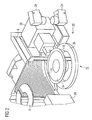
- Fig. 1
- schematisch eine Anlage zum Ausführen des erfindungsgemäßen Verfahrens,
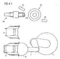
- Fig. 2
- schematisch und in Schrägansicht eine Inspektionsstation der Anlage von Fig. 1,
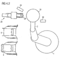
- Fig. 3
- das Prinzip des optischen Sensors der Inspektionsstation, und
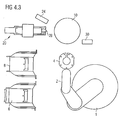
- Fig. 4
- in einer Abfolge von sieben Bildern die Schritte beim Kontrollieren des Randes eines Wafers, bspw. eines 8-Zoll-Wafers.
Claims (18)
- Verfahren zum automatischen Kontrollieren des Randes (16) eines scheibenförmigen Gegenstandes (10), insbesondere eines Wafers (10), dadurch gekennzeichnet, dass Bilder der Oberseite und/oder der Unterseite im Randbereich des Gegenstandes aufgenommen werden.
- Verfahren nach Anspruch 1, dadurch gekennzeichnet, dass der Gegenstand (10) während des Erzeugens der Bilder seines Randes (16) kontinuierlich gedreht wird,
dass die Bilder der Unterseite und der Oberseite gleichzeitig aufgenommen werden,
und/oder dass ein mittlerer Bereich der Oberseite und der Unterseite nicht aufgenommen wird. - Verfahren nach Anspruch 1 oder 2, dadurch gekennzeichnet, dass während des Aufnehmens der Bilder der Ober- und/oder der Unterseite des Randes (16) des Gegenstandes (10) Relativbewegungen des Randes (16) des Gegenstandes (10) relativ zum Mittelpunkt der Drehung kompensiert werden.
- Verfahren nach einem der Ansprüche 1 bis 3, dadurch gekennzeichnet, dass ein etwa 2 mm breiter Randbereich des Gegenstandes (10) kontrolliert wird.
- Verfahren nach einem der Ansprüche 1 bis 4, dadurch gekennzeichnet, dass ermittelte Fehlstellen klassifiziert werden, insbesondere in Muschelausbruch und Haarriss.
- Verfahren nach einem der Ansprüche 1 bis 5, dadurch gekennzeichnet, dass Art und Lage der Beschädigung des Gegenstandes (10) in einer Datei gespeichert werden.
- Verfahren nach einem der Ansprüche 1 bis 6, dadurch gekennzeichnet, dass vor oder nach oder beim Aufnehmen der Bilder des Randes (16) des Gegenstandes (10) der Verlauf des Randes (16) des Gegenstandes (10) relativ zu dem Mittelpunkt erfasst wird, um den der Gegenstand (10) beim Aufnehmen gedreht wird.
- Verfahren nach einem der Ansprüche 1 bis 7, dadurch gekennzeichnet, dass vor dem Aufnehmen der Bilder des Randes (16) des Gegenstandes (10) die Lage einer Markierung (14) am Rand (16) des Gegenstandes (10) erfasst wird, wie einer abgeflachten Stelle oder einer Kerbe am Rand eines Wafers (10).
- Verfahren nach einem der Ansprüche 1 bis 8, dadurch gekennzeichnet, dass ein Gegenstand (10) nach dem Kontrollieren des Randes (16) positionskorrigiert abgelegt wird, insbesondere auf einem Greifer (4), der ihn zu einer Ausgangs-Horde (8) bewegt.
- Vorrichtung zum Kontrollieren des Randes (16) eines scheibenförmigen Gegenstandes (10) zum Durchführen des Verfahrens nach einem der Ansprüche 1 bis 9, gekennzeichnet durch einen Greifer (4), der an einem Bewegungsroboter (1) vorgesehen ist, durch eine Inspektionsstation (10) mit einem Sensor (28) zum Erzeugen von Bildern des Randes (16) des Gegenstandes (10) und mit einem Träger (22) zum Drehen des Gegenstandes (10) relativ zum Sensor (28).
- Vorrichtung nach Anspruch 10, dadurch gekennzeichnet, dass in der Inspektionsstation (20) ein Liniensensor (24) zum Erfassen des Verlaufes des Randes (16) des Gegenstandes (10) beim Drehen desselben auf dem Inspektionschuck (22) vorgesehen ist.
- Vorrichtung nach Anspruch 10 oder 11, dadurch gekennzeichnet, dass in der Inspektionsstation (20) ein Strichcodeleser (30) zum Lesen des Strichcodes auf dem Gegenstand (10) vorgesehen ist.
- Vorrichtung nach einem der Ansprüche 10 bis 12, dadurch gekennzeichnet, dass der Sensor (28) ein optischer Sensor (28) ist,
und/oder dass der optische Sensor (28) auf einem Linearschlitten (26) montiert ist, über den er radial zum Inspektionschuck (22) verstellbar ist. - Vorrichtung nach Anspruch 13, dadurch gekennzeichnet, dass der Antrieb für den Linearschlitten (26) unter Ausnutzung der vom Linearsensor (24) erfassten Daten über den Verlauf des Randes (16) des Gegenstandes (10) gesteuert ist.
- Vorrichtung nach einem der Ansprüche 10 bis 14, dadurch gekennzeichnet, dass der Sensor (28) zwei symmetrische Wege (42, 44) enthält,
und/oder dass ein CCD-Sensor (40), insbesondere ein Linien-CCD-Sensor, vorgesehen ist, auf dem vorzugsweise beide Seiten des Randes (16) des Gegenstandes (10) gleichzeitig abgebildet werden. - Vorrichtung nach einem der Ansprüche 10 bis 15, dadurch gekennzeichnet, dass der Sensor (28) zwei Strahlungsquellen (46) enthält, insbesondere zwei Lichtquellen (46), die Strahlung auf den Rand (16) des Gegenstandes (10) von oben und von unten her durch Strahlteiler (50) abgeben,
und/oder dass vom Rand (16) des Gegenstandes (10) reflektierte Strahlung durch die Strahlteiler (50) vorzugsweise über ein Linsen-/Spiegel-System (42, 44) dem Sensor (40) zugeleitet wird. - Vorrichtung nach einem der Ansprüche 10 bis 16, dadurch gekennzeichnet, dass der Greifer (4) am Handhabungsroboter (1) als Dünnwafergreifer ausgebildet ist.
- Vorrichtung nach einem der Ansprüche 10 bis 17, dadurch gekennzeichnet, dass der in der Inspektionsstation (20) vorgesehene Träger (22) einen zentral angeordneten Hilfsträger und zwei wahlweise einsetzbare Zusatzträger (34, 36) aufweist.
Applications Claiming Priority (2)
| Application Number | Priority Date | Filing Date | Title |
|---|---|---|---|
| DE10303459 | 2003-01-29 | ||
| DE10303459A DE10303459A1 (de) | 2003-01-29 | 2003-01-29 | Verfahren und Vorrichtung zum Kontrollieren des Randes eines scheibenförmigen Gegenstandes |
Publications (3)
| Publication Number | Publication Date |
|---|---|
| EP1443542A2 true EP1443542A2 (de) | 2004-08-04 |
| EP1443542A3 EP1443542A3 (de) | 2005-12-21 |
| EP1443542B1 EP1443542B1 (de) | 2008-02-27 |
Family
ID=32603020
Family Applications (1)
| Application Number | Title | Priority Date | Filing Date |
|---|---|---|---|
| EP04001554A Expired - Lifetime EP1443542B1 (de) | 2003-01-29 | 2004-01-26 | Verfahren und Vorrichtung zum Kontrollieren des Randes eines scheibenförmigen Gegenstandes |
Country Status (2)
| Country | Link |
|---|---|
| EP (1) | EP1443542B1 (de) |
| DE (2) | DE10303459A1 (de) |
Cited By (4)
| Publication number | Priority date | Publication date | Assignee | Title |
|---|---|---|---|---|
| DE102004058126A1 (de) * | 2004-12-02 | 2006-06-08 | Leica Microsystems Jena Gmbh | Vorrichtung zur Inspektion der Vorder- und Rückseite eines scheibenförmigen Objekts |
| CN106532945A (zh) * | 2016-11-30 | 2017-03-22 | 河海大学常州校区 | 一种机器人电站巡检系统及方法 |
| CN114670352A (zh) * | 2022-05-26 | 2022-06-28 | 广东高景太阳能科技有限公司 | 一种实时自动控制的硅片生产方法、系统、介质及设备 |
| CN115791807A (zh) * | 2023-01-09 | 2023-03-14 | 苏州高视半导体技术有限公司 | 用于检测晶圆缺陷的装置 |
Families Citing this family (3)
| Publication number | Priority date | Publication date | Assignee | Title |
|---|---|---|---|---|
| DE102004058128B4 (de) * | 2004-12-02 | 2008-05-15 | Vistec Semiconductor Systems Jena Gmbh | System zur Inspektion eines scheibenförmigen Objekts |
| DE102005014596B3 (de) * | 2005-03-31 | 2007-01-04 | Leica Microsystems Jena Gmbh | Vorrichtung und Verfahren zur Inspektion der Oberfläche eines Wafers |
| US11600504B2 (en) * | 2020-06-29 | 2023-03-07 | Taiwan Semiconductor Manufacturing Company, Ltd. | Detecting damaged semiconductor wafers utilizing a semiconductor wafer sorter tool of an automated materials handling system |
Family Cites Families (8)
| Publication number | Priority date | Publication date | Assignee | Title |
|---|---|---|---|---|
| IL86514A0 (de) * | 1988-05-26 | 1988-11-15 | ||
| US5238354A (en) * | 1989-05-23 | 1993-08-24 | Cybeq Systems, Inc. | Semiconductor object pre-aligning apparatus |
| JP2000512564A (ja) * | 1996-06-15 | 2000-09-26 | ウノバ・ユー・ケイ・リミテッド | プラットホームに柔軟に取付けられた研削マシンスピンドル |
| GB2337111B (en) * | 1996-06-15 | 2000-03-15 | Unova Uk Ltd | Workpiece inspection |
| JPH1096700A (ja) * | 1996-09-20 | 1998-04-14 | Nikon Corp | 異物検査装置 |
| IL123575A (en) * | 1998-03-05 | 2001-08-26 | Nova Measuring Instr Ltd | Method and apparatus for alignment of a wafer |
| JP2000046537A (ja) * | 1998-07-24 | 2000-02-18 | Kobe Steel Ltd | 欠陥検査装置 |
| EP1001460B1 (de) * | 1998-10-15 | 2001-05-02 | Wacker Siltronic Gesellschaft für Halbleitermaterialien Aktiengesellschaft | Verfahren und Vorrichtung zum Detektieren, Überwachung und Charakterisierung von Kantendefekten in Halbleiterscheiben |
-
2003
- 2003-01-29 DE DE10303459A patent/DE10303459A1/de not_active Ceased
-
2004
- 2004-01-26 EP EP04001554A patent/EP1443542B1/de not_active Expired - Lifetime
- 2004-01-26 DE DE502004006284T patent/DE502004006284D1/de not_active Expired - Lifetime
Cited By (5)
| Publication number | Priority date | Publication date | Assignee | Title |
|---|---|---|---|---|
| DE102004058126A1 (de) * | 2004-12-02 | 2006-06-08 | Leica Microsystems Jena Gmbh | Vorrichtung zur Inspektion der Vorder- und Rückseite eines scheibenförmigen Objekts |
| CN106532945A (zh) * | 2016-11-30 | 2017-03-22 | 河海大学常州校区 | 一种机器人电站巡检系统及方法 |
| CN106532945B (zh) * | 2016-11-30 | 2019-07-19 | 河海大学常州校区 | 一种机器人电站巡检系统及方法 |
| CN114670352A (zh) * | 2022-05-26 | 2022-06-28 | 广东高景太阳能科技有限公司 | 一种实时自动控制的硅片生产方法、系统、介质及设备 |
| CN115791807A (zh) * | 2023-01-09 | 2023-03-14 | 苏州高视半导体技术有限公司 | 用于检测晶圆缺陷的装置 |
Also Published As
| Publication number | Publication date |
|---|---|
| EP1443542A3 (de) | 2005-12-21 |
| DE10303459A1 (de) | 2004-08-19 |
| DE502004006284D1 (de) | 2008-04-10 |
| EP1443542B1 (de) | 2008-02-27 |
Similar Documents
| Publication | Publication Date | Title |
|---|---|---|
| DE102007010225B4 (de) | Verfahren zur Aufnahme von hochauflösenden Bildern von Defekten auf der Oberseite des Waferrandes | |
| DE102014208768B4 (de) | Verfahren und Vorrichtung zur Qualitätssicherung | |
| DE3917260A1 (de) | Waferinspektionseinrichtung | |
| DE102020201863A1 (de) | Einspanntisch und Untersuchungsvorrichtung | |
| DE102020200257A1 (de) | Werkstückschneidverfahren | |
| DE10304174A1 (de) | Vorrichtung und Verfahren zur Waferrückseiteninspektion | |
| DE102018212588A1 (de) | Waferbearbeitungsverfahren | |
| DE102016011497B4 (de) | Optische Untersuchungseinrichtung und optisches Untersuchungsverfahren mit sichtbarem und infrarotem Licht für Halbleiterbauteile | |
| DE19809505A1 (de) | Einrichtung zum Prüfen optischer Elemente | |
| DE69526813T2 (de) | Vorrichtung zur Messung des Durchmessers und der Form des Querschnitts eines Wafers | |
| DE19708582A1 (de) | Qualitätskontrolle für Kunststeine | |
| WO1989008836A1 (fr) | Procede et dispositif de detection de defauts dans des pieces embouties a la piece ou dans d'autres pieces a usiner | |
| DE102022204693A1 (de) | Schutzfilm-dickenmessverfahren | |
| DE10324474A1 (de) | Vorrichtung zur Wafer-Inspektion | |
| DE102022205753A1 (de) | Betriebsgenauigkeit-messverfahren | |
| EP1443542A2 (de) | Verfahren und Vorrichtung zum Kontrollieren des Randes eines scheibenförmigen Gegenstandes | |
| WO2008113638A2 (de) | Vorrichtung und verfahren zur inspektion von defekten am randbereich eines wafers und verwendung der vorrichtung in einer inspektionseinrichtung für wafer | |
| EP0528197A1 (de) | Verfahren und Vorrichtung zur Inspektion von Tabletten | |
| DE102019125134B4 (de) | Vorrichtung und Verfahren zur Bauteilhandhabung | |
| EP3655175A1 (de) | Verfahren zum betrieb einer bearbeitungsanlage mit beweglichem stempel | |
| DE4124278A1 (de) | Verfahren und vorrichtung zur inspektion von tabletten | |
| DE102019125127A1 (de) | Bauteilhandhabung, Bauteilinspektion | |
| DE10232781B4 (de) | Vorrichtung zur Wafer-Inspektion | |
| DE102022111903A1 (de) | Inspektion bei der Herstellung von Modulen oder Vorstufen von Modulen | |
| EP4466745B1 (de) | Inspektion bei der herstellung von modulen oder vorstufen von modulen |
Legal Events
| Date | Code | Title | Description |
|---|---|---|---|
| PUAI | Public reference made under article 153(3) epc to a published international application that has entered the european phase |
Free format text: ORIGINAL CODE: 0009012 |
|
| AK | Designated contracting states |
Kind code of ref document: A2 Designated state(s): AT BE BG CH CY CZ DE DK EE ES FI FR GB GR HU IE IT LI LU MC NL PT RO SE SI SK TR |
|
| AX | Request for extension of the european patent |
Extension state: AL LT LV MK |
|
| RIN1 | Information on inventor provided before grant (corrected) |
Inventor name: KROUPA, GERHARD Inventor name: BINDER, ALFRED Inventor name: VON KOBLINSKI, CARSTEN, DR. Inventor name: MATSCHITSCH, MARTIN |
|
| PUAL | Search report despatched |
Free format text: ORIGINAL CODE: 0009013 |
|
| AK | Designated contracting states |
Kind code of ref document: A3 Designated state(s): AT BE BG CH CY CZ DE DK EE ES FI FR GB GR HU IE IT LI LU MC NL PT RO SE SI SK TR |
|
| AX | Request for extension of the european patent |
Extension state: AL LT LV MK |
|
| 17P | Request for examination filed |
Effective date: 20060317 |
|
| AKX | Designation fees paid |
Designated state(s): DE FR GB |
|
| 17Q | First examination report despatched |
Effective date: 20060807 |
|
| GRAP | Despatch of communication of intention to grant a patent |
Free format text: ORIGINAL CODE: EPIDOSNIGR1 |
|
| GRAS | Grant fee paid |
Free format text: ORIGINAL CODE: EPIDOSNIGR3 |
|
| GRAA | (expected) grant |
Free format text: ORIGINAL CODE: 0009210 |
|
| AK | Designated contracting states |
Kind code of ref document: B1 Designated state(s): DE FR GB |
|
| REG | Reference to a national code |
Ref country code: GB Ref legal event code: FG4D Free format text: NOT ENGLISH |
|
| REF | Corresponds to: |
Ref document number: 502004006284 Country of ref document: DE Date of ref document: 20080410 Kind code of ref document: P |
|
| ET | Fr: translation filed | ||
| PLBE | No opposition filed within time limit |
Free format text: ORIGINAL CODE: 0009261 |
|
| STAA | Information on the status of an ep patent application or granted ep patent |
Free format text: STATUS: NO OPPOSITION FILED WITHIN TIME LIMIT |
|
| 26N | No opposition filed |
Effective date: 20081128 |
|
| GBPC | Gb: european patent ceased through non-payment of renewal fee |
Effective date: 20090126 |
|
| PG25 | Lapsed in a contracting state [announced via postgrant information from national office to epo] |
Ref country code: GB Free format text: LAPSE BECAUSE OF NON-PAYMENT OF DUE FEES Effective date: 20090126 |
|
| REG | Reference to a national code |
Ref country code: FR Ref legal event code: PLFP Year of fee payment: 13 |
|
| REG | Reference to a national code |
Ref country code: FR Ref legal event code: PLFP Year of fee payment: 14 |
|
| REG | Reference to a national code |
Ref country code: FR Ref legal event code: PLFP Year of fee payment: 15 |
|
| PGFP | Annual fee paid to national office [announced via postgrant information from national office to epo] |
Ref country code: DE Payment date: 20210329 Year of fee payment: 18 |
|
| PGFP | Annual fee paid to national office [announced via postgrant information from national office to epo] |
Ref country code: FR Payment date: 20220119 Year of fee payment: 19 |
|
| REG | Reference to a national code |
Ref country code: DE Ref legal event code: R119 Ref document number: 502004006284 Country of ref document: DE |
|
| PG25 | Lapsed in a contracting state [announced via postgrant information from national office to epo] |
Ref country code: DE Free format text: LAPSE BECAUSE OF NON-PAYMENT OF DUE FEES Effective date: 20220802 |
|
| PG25 | Lapsed in a contracting state [announced via postgrant information from national office to epo] |
Ref country code: FR Free format text: LAPSE BECAUSE OF NON-PAYMENT OF DUE FEES Effective date: 20230131 |