EP1441457A1 - Direct conversion receiver - Google Patents
Direct conversion receiver Download PDFInfo
- Publication number
- EP1441457A1 EP1441457A1 EP02777966A EP02777966A EP1441457A1 EP 1441457 A1 EP1441457 A1 EP 1441457A1 EP 02777966 A EP02777966 A EP 02777966A EP 02777966 A EP02777966 A EP 02777966A EP 1441457 A1 EP1441457 A1 EP 1441457A1
- Authority
- EP
- European Patent Office
- Prior art keywords
- frequency
- signal
- fft
- receiving object
- converting
- Prior art date
- Legal status (The legal status is an assumption and is not a legal conclusion. Google has not performed a legal analysis and makes no representation as to the accuracy of the status listed.)
- Withdrawn
Links
Images







Classifications
-
- H—ELECTRICITY
- H04—ELECTRIC COMMUNICATION TECHNIQUE
- H04B—TRANSMISSION
- H04B1/00—Details of transmission systems, not covered by a single one of groups H04B3/00 - H04B13/00; Details of transmission systems not characterised by the medium used for transmission
- H04B1/0003—Software-defined radio [SDR] systems, i.e. systems wherein components typically implemented in hardware, e.g. filters or modulators/demodulators, are implented using software, e.g. by involving an AD or DA conversion stage such that at least part of the signal processing is performed in the digital domain
- H04B1/0028—Software-defined radio [SDR] systems, i.e. systems wherein components typically implemented in hardware, e.g. filters or modulators/demodulators, are implented using software, e.g. by involving an AD or DA conversion stage such that at least part of the signal processing is performed in the digital domain wherein the AD/DA conversion occurs at baseband stage
- H04B1/0032—Software-defined radio [SDR] systems, i.e. systems wherein components typically implemented in hardware, e.g. filters or modulators/demodulators, are implented using software, e.g. by involving an AD or DA conversion stage such that at least part of the signal processing is performed in the digital domain wherein the AD/DA conversion occurs at baseband stage with analogue quadrature frequency conversion to and from the baseband
-
- H—ELECTRICITY
- H04—ELECTRIC COMMUNICATION TECHNIQUE
- H04B—TRANSMISSION
- H04B1/00—Details of transmission systems, not covered by a single one of groups H04B3/00 - H04B13/00; Details of transmission systems not characterised by the medium used for transmission
- H04B1/0003—Software-defined radio [SDR] systems, i.e. systems wherein components typically implemented in hardware, e.g. filters or modulators/demodulators, are implented using software, e.g. by involving an AD or DA conversion stage such that at least part of the signal processing is performed in the digital domain
-
- H—ELECTRICITY
- H04—ELECTRIC COMMUNICATION TECHNIQUE
- H04B—TRANSMISSION
- H04B1/00—Details of transmission systems, not covered by a single one of groups H04B3/00 - H04B13/00; Details of transmission systems not characterised by the medium used for transmission
- H04B1/06—Receivers
- H04B1/16—Circuits
- H04B1/30—Circuits for homodyne or synchrodyne receivers
-
- H—ELECTRICITY
- H04—ELECTRIC COMMUNICATION TECHNIQUE
- H04L—TRANSMISSION OF DIGITAL INFORMATION, e.g. TELEGRAPHIC COMMUNICATION
- H04L27/00—Modulated-carrier systems
- H04L27/26—Systems using multi-frequency codes
- H04L27/2601—Multicarrier modulation systems
- H04L27/2647—Arrangements specific to the receiver only
Definitions
- the present invention relates to a direct conversion receiver, and more particularly, to a direct conversion receiver that can be utilized for partial receiving for receiving only one segment in terrestrial digital TV broadcasting.
- an OFDM (Orthogonal Frequency Division Multiplexing) method has been proposed as a method superior in high-quality transmission and improvement in frequency utilization efficiency.
- the OFDM method is a modulation method for causing a lot of sub-carriers to stand in a band including one channel.
- an analog TV signal is converted into a digital signal, and the digital signal is then subjected to data compression by MPEG (Moving Picture Expert Group).
- a data signal thus obtained is subjected to byte interleaving and bit interleaving so as to distribute the cause of errors in a transmission path, for example, noises, and is subjected to mapping corresponding to a modulation method such as QPSK (Quadrature Phase Shift Keying) and 16 QAM (Quadrature Amplitude Modulation).
- QPSK Quadrature Phase Shift Keying
- 16 QAM Quadrature Amplitude Modulation
- Data obtained by the mapping is subjected to time interleaving and frequency interleaving for dispersing the cause of errors in a transmission path, for example, fading, is then subjected to IFFT (inverse fast Fourier transform), is subjected to orthogonal modulation, is then frequency-converted into an RF frequency, and is transmitted.
- IFFT inverse fast Fourier transform
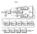
- Fig. 1 illustrates the configuration of a digital television receiver.
- An RF signal received by an antenna is inputted to a mixer 21.
- a signal corresponding to channel selection is also inputted to the mixer 21 from a local signal generator 22, and a signal obtained by frequency conversion is outputted such that a desired frequency falls within a band of a BPF (Band-Pass Filter) 23.
- BPF Band-Pass Filter
- Outputs of the BPF 23 are respectively inputted to mixers 24 and 25.
- a cosine signal and a sine signal are respectively inputted from a 90-degree phase shifter 27 having as an input a signal from a local signal generator 26.
- the mixers 24 and 25 respectively down-convert the outputs of the BPF 23 which are IF (Intermediate Frequency) signals, convert the down-converted outputs into Low IF signals each comprising a real axis (I axis) component and an imaginary axis (Q axis) component, and output the Low IF signals to analog-to-digital converters 7 and 8.
- an analog signal (an I axis component and a Q axis component) is converted into a digital signal, and the digital signal is outputted to an FFT circuit 9.
- the input signal is subjected to fast Fourier transform (FFT), to transform the signal from time axis data to frequency axis data and output the signal to a frequency de-interleave circuit 12.
- FFT fast Fourier transform
- frequency interleaving carried out in order to compensate for a signal having a particular frequency which is missing due to the reflection of electro-magnetic waves, for example, is released.
- An output of the frequency de-interleave circuit 12 is fed to a time de-interleave circuit 13.
- The-time de-interleave circuit 13 releases time interleaving carried out for fading resistance or the like.
- An I-axis and Q-axis signal obtained by the time deinterleaving is fed to a de-mapping circuit 14, and is decoded into 2 bits (QPSK), 4 bits (16 QAM), or 6 bits (64 QAM).
- a signal obtained by de-mapping is fed to a bit de-interleave circuit 15.
- the bit de-interleave circuit 15 releases bit interleaving carried out for the purpose of increasing error resistance.
- An output of the bit de-interleave circuit 15 is fed to a Viterbi decoding circuit 16.
- the Viterbi decoding circuit 16 makes error correction using a convolutional code generated on the transmission side.
- a signal obtained by Viterbi decoding is fed to a byte de-interleave circuit 17.
- the byte de-interleave circuit 17 releases byte interleaving carried out for the purpose of increasing error resistance, similarly to bit interleaving.
- An output of the byte de-interleave circuit 17 is fed to an RS decoding circuit 18.
- the RS decoding circuit 18 performs RS (Reed-Solomon) decoding to make error correction.
- a signal obtained by the error correction is fed to an MPEG decoding circuit 19.
- the MPEG decoding circuit 19 extends a signal obtained by the error correction (a compressed signal), and outputs the extended signal to a digital-to-analog conversion circuit 20.
- the digital-to-analog conversion circuit 20 converts the signal fed from the MPEG decoding circuit 19 into an analog video/analog audio signal, and outputs the signal.
- a segment-divided signal format is employed.
- 13 segments are collectively transmitted into a band of 6 MHz.
- such partial receiving that data broadcasting or the like can be performed by only the one segment is possible.
- the band width is only reduced to one-thirteenth in the partial receiving, so that receiving is possible in approximately the same configuration.
- Fig. 2 illustrates a spectrum in each of the blocks shown in Fig. 1 in a case where partial receiving is performed.
- Fig. 2 (a) illustrates a spectrum of an RF (Radio Frequency) signal corresponding to terrestrial digital broadcasting (UHF).
- UHF terrestrial digital broadcasting
- a spectrum corresponding to UHF Channels 14 to 16 is illustrated.
- One channel has a band width of 6 HMz, and is composed of 13 segments. The segment at the center out of the segments corresponds to a signal for partial receiving.
- Fig. 2 (b) illustrates a spectrum of the RF signal corresponding to the UHF Channel 15, where the spectrum corresponds to the six segments S15-0 to S15-6 at the center out of the 13 segments.
- Fig. 2 (c) illustrates a spectrum of an IF signal corresponding to the UHF Channel 15 outputted from the mixer 21, where the spectrum corresponds to the six segments S15-0 to S15-6 at the center out of the 13 segments.
- Fig. 2 (d) illustrates a spectrum of the IF signal outputted from the BPF 23 in the case of partial receiving.
- a partial receiving object segment S15-0 at the center in the spectrum of the IF signal corresponding to the UHF Channel 15 is extracted by the BPF 23.
- Fig. 2 (e) illustrates a spectrum of a Low IF signal outputted from the mixer 24 or 25 at the time of partial receiving.
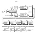
- Fig. 3 illustrates the configuration of a conventional receiver using a direct conversion system.
- the same blocks as those shown in Fig. 1 are assigned the same reference numerals and hence, the description thereof is not repeated.
- the difference between the conventional receiver using a direct conversion system and the receiver using a super heterodyne system shown in Fig. 1 is as follows:
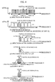
- Fig. 4 illustrates a spectrum in each of the units shown in Fig. 3.
- Fig. 4 (a) illustrates.a spectrum of an RF signal corresponding to terrestrial digital broadcasting (UHF).
- Fig. 4 (b) is an enlarged view of the UHF Channel 15, which illustrates, taking a partial receiving object segment as S15-0 and taking segments in the lower and upper bands than the partial receiving object segment as S15-1 to S15-12, the segments S15-0 to S15-6.
- Fig. 4 (c) illustrates a spectrum after the frequency conversion by the down converter (the local signal generator 1, the mixers 2 and 3, and the 90-degree phase shifter 4).
- the down converter frequency-converts the RF signal such that the center frequency of the occupied band of the partial receiving object segment S15-0 is a frequency of zero (a DC component). Accordingly, the RF signal is folded back at a frequency which is one-half the occupied band of the partial receiving object segment S15-0, and the folded signal is multiplexed.
- Fig. 4 (d) illustrates a spectrum after removal of frequency components (unnecessary components) higher than the partial receiving object segment S15-0 by the LPFs 5 and 6.
- Fig. 4 (e) illustrates a spectrum after transformation from time axis data to frequency axis data in an FFT circuit 9, where only a signal corresponding to the partial receiving object segment S15-0 is obtained.
- An object of the present invention is to provide a direct conversion receiver that eliminates the necessity of using a steep analog filter so as to remove an unnecessary component other than a receiving object segment.
- Another object of the present invention is to provide, in a direct conversion receiver for frequency-converting an RF signal such that the center frequency of the occupied band is a frequency of zero (a DC component), a direct conversion receiver in which high-precision DC offset correction is possible in a simple configuration.
- a further object of the present invention is to provide a direct conversion receiver capable of reducing the circuit scale.
- a first direct conversion receiver is characterized by comprising a down converter for frequency-converting an analog RF signal modulated by an OFDM method such that the center frequency of the occupied band of a segment which is a receiving object (hereinafter referred to as a receiving object segment) is a frequency of zero; AD conversion means for converting a down converted signal obtained by the down converter into a digital signal; FFT means for subjecting the signal obtained by the AD conversion means to fast Fourier transform, to transform the signal from time axis data to frequency axis data; and unnecessary component removal means for removing from an output signal of the FFT means an unnecessary component other than the receiving object segment.
- a second direct conversion receiver is characterized by comprising a down converter for frequency-converting an analog RF signal modulated by an OFDM method such that the center frequency of the occupied band of a receiving object segment is a frequency of zero; filter means for removing a high-frequency component from a down converted signal obtained by the down converter; AD conversion means for converting an output signal of the filter means into a digital signal; FFT means for subjecting the signal obtained by the AD conversion means to fast Fourier transform; and unnecessary component removal means for removing from an output signal of the FFT means an unnecessary component other than the receiving object segment.
- the above-mentioned first or second direct conversion receiver is provided with DC offset detection means for detecting a DC offset amount from a DC component after the fast Fourier transform carried out by the FFT means, and DC offset correction means for correcting DC offset on the basis of the DC offset amount detected by the DC offset detection means.
- An example of the DC offset detection means is one for integrating the DC component after the fast Fourier transform carried out by the FFT means for a predetermined time period, and taking an obtained integrated value as an offset amount.
- An example of the DC offset detection means is one comprising difference means having a plurality of reference values and calculating and outputting a difference value between the DC component after the fast Fourier transform carried out by the FFT means and each of the reference values, comparison means for selecting and outputting the minimum value of the difference values calculated by the difference means, and integration means for integrating the difference value outputted by the comparison means for a predetermined time period and outputting an obtained integrated value as an offset amount.
- a third direct conversion receiver is characterized by comprising a down converter for frequency-converting an analog RF signal modulated by an OFDM method such that the upper-end frequency or the lower-end frequency of the occupied band of a receiving object segment is in the vicinity of a frequency of zero; AD cohversion means for converting a down converted signal obtained by the down converter into a digital signal; FFT means for subjecting the signal obtained by the AD conversion means to fast Fourier transform, to transform the signal from time axis data to frequency axis data; and unnecessary component removal means for removing from an output signal of the FFT means an unnecessary component other than the receiving object segment.
- a fourth direct conversion receiver is characterized by comprising a down converter for frequency-converting an analog RF signal modulated by an OFDM method such that the upper-end frequency or the lower-end frequency of the occupied band of a receiving object segment is in the vicinity of a frequency of zero; filter means for removing a high-frequency component from a down converted signal obtained by the down converter; AD conversion means for converting an output signal of the filter means into a digital signal; FFT means for subjecting the signal obtained by the AD conversion means to fast Fourier transform, to transform the signal from time axis data to frequency axis data; and unnecessary component removal means for removing from an output signal of the FFT means an unnecessary component other than the receiving object segment.
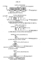
- Fig. 5 illustrates the configuration of a digital television receiver for performing partial receiving.
- Fig. 6 illustrates a spectrum in each of blocks shown in Fig. 5.
- a signal is transmitted by a spectrum as illustrated in Fig. 6 (a).
- Fig. 6 (a) a spectrum corresponding to UHF Channels 14 to 16 is illustrated.
- One channel has a band width of 6 HMz, and is composed of 13 segments. The segment at the center out of the 13 segments corresponds to a signal for partial receiving, by which partial receiving is possible. Description is made of a case where the UHF Channel 15 is partially received.
- Fig. 6 (b) is an enlarged view of the UHF Channel 15, which illustrates, taking a segment which is a partial. receiving object (hereinafter referred to as a partial receiving object segment) as S15-0 and taking segments in the lower and upper bands than the partial receiving object segment as S15-1 to S15-12, the segments S15-0 to S15-6.
- a partial receiving object segment a segment which is a partial. receiving object (hereinafter referred to as a partial receiving object segment) as S15-0 and taking segments in the lower and upper bands than the partial receiving object segment as S15-1 to S15-12, the segments S15-0 to S15-6.
- An RF signal corresponding to the UHF Channel 15 is frequency-converted by a down converter (a local signal generator 1, a 90-degree phase shifter 4, and mixers 2 and 3) shown in Fig. 5.
- a signal having a frequency for frequency-converting the RF signal is outputted from the local signal generator 1 such that the center frequency of the occupied band of the partial receiving object segment S15-0 becomes a frequency of zero.
- a cosine signal and a sine signal are respectively outputted to the mixers 2 and 3 from the 90-degree phase shifter 4 so as to output a real axis component and an imaginary axis component.
- a spectrum after the frequency conversion by the down converter is as illustrated in Fig. 6 (c).
- the down converter frequency-converts the RF signal such that the center frequency of the occupied band of the partial receiving object segment S15-0 becomes a frequency of zero (a DC component). Accordingly, the RF signal is folded back at a frequency which is one-half the occupied band of the partial receiving object segment S15-0, and the folded signal is multiplexed.
- Harmonic components of the signal are respectively removed by the LPFs 5 and 6.
- a spectrum of output signals after the removal of the harmonic components by the LPFs 5 and 6 is as illustrated in Fig. 6 (d).
- An analog filter having gentler characteristics, as compared with those in the conventional example, is used as the LPFs 5 and 6. In the spectrum of the output signals after the removal of the harmonic components by the LPFs 5 and 6, therefore, not only the partial receiving object segment S15-0 but also the segments S15-1 and S15-2 adjacent thereto remain.
- the signals are transformed from time axis data to frequency axis data in an FFT circuit 9.
- a spectrum of output signals of the FFT circuit 9 is as illustrated in Fig. 6 (e).
- the output signals of the FFT circuit 9 are outputted to a frequency de-interleave circuit 12 after the segments S15-1 to S15-2 which are unnecessary components other than the partial receiving object segment S15-0 are respectively removed therefrom in the unnecessary component removal circuits 10 and 11. Consequently, a spectrum of the output signals of the unnecessary component removal circuits 10 and 11 is only the partial receiving object segment S15-0, as illustrated in Fig. 6 (f).
- Signal processing in the succeeding stage of the frequency de-interleave circuit 12 is the same as that in the receiver shown in Fig. 1.
- a to B denote the amplitudes of the signal.
- the signal is multiplied by cos(- ⁇ t) -jsin(- ⁇ t) and integrated for one period, to obtain A, while being multiplied by cos( ⁇ t) - jsin( ⁇ t) and integrated for one period, to obtain B. Accordingly, a positive frequency component and a negative frequency component can be completely separated from each other.
- the necessity of using a steep analog filter so as to remove unnecessary components other than the receiving object segment is eliminated.
- Fig. 7 illustrates the configuration of a digital television receiver using a direct conversion system.
- Fig. 8 illustrates a spectrum in each of blocks shown in Fig. 7.
- a signal is transmitted by a spectrum as illustrated in Fig. 8 (a).
- Fig. 8 (a) a spectrum corresponding to UHF Channels 14 to 16 is illustrated.
- One channel has a band width of 6 HMz, and is composed of 13 segments. The segment at the center out of the segments corresponds to a signal for partial receiving. Description is made of a case where the UHF Channel 15 is partially received.
- Fig. 8 (b) is an enlarged view of the UHF Channel 15, which illustrates, taking a partial receiving object segment as S15-0 and taking segments in the lower and upper bands than the partial receiving object segment as S15-1 to S15-12, the segments S15-0 to S15-6.
- An RF signal corresponding to the UHF Channel 15 is frequency-converted by a down converter (a local signal generator 1, a 90-degree phase shifter 4, and mixers 2 and 3) shown in Fig. 7.
- a signal having a frequency for frequency-converting the RF signal is outputted from the local signal generator 1 such that the center frequency of the occupied band of the partial receiving object segment S15-0 becomes a frequency of zero.
- a cosine signal and a sine signal are respectively outputted to the mixers 2 and 3 from the 90-degree phase shifter 4 so as to output a real axis component and an imaginary axis component.
- a spectrum after the frequency conversion by the down converter is as illustrated in Fig. 8 (c).
- the down converter frequency-converts the RF signal such that the center frequency of the occupied band of the partial receiving object segment S15-0 is a frequency of zero (a DC component). Accordingly, the RF signal is folded back at a frequency which is one-half the occupied band of the partial receiving object segment S15-0, and the folded signal is multiplexed.
- Harmonic components of the signal are respectively removed by the LPFs 5 and 6.
- a spectrum of output signals after the removal of the harmonic components by the LPFs 5 and 6 is as illustrated in Fig. 8 (d).
- An analog filter having relatively gentle characteristics is used as the LPFs 5 and 6. In the spectrum of the output signals after the removal of the harmonic components by the LPFs 5 and 6, therefore, not only the partial receiving object segment S15-0 but also the segments S15-1 and S15-2 adjacent thereto remain.
- the signals are transformed from time axis data to frequency axis data in an FFT circuit 9.
- a spectrum of output signals of the FFT circuit 9 is as illustrated in Fig. 8 (e).
- the output signals of the FFT circuit 9 are outputted to a frequency de-interleave circuit 12 after the segments S15-1 and S15-2 which are unnecessary components other than the partial receiving object segment S15-0 are respectively removed therefrom in the unnecessary component removal circuits 10 and 11. Consequently, a spectrum of output signals of the unnecessary component removal circuits 10 and 11 is only the partial receiving object segment S15-0, as illustrated in Fig. 8 (f).
- Signal processing in the succeeding stage of the frequency de-interleave circuit 12 is the same as that in the receiver shown in Fig. 1.
- a DC component (a component having a frequency of zero) is also a signal component, so that a signal having no DC offset is required.
- Examples of the cause of DC offset include DC offset of an active element in a case where the mixers 2 and 3 and the LPFs 5 and 6 are active filters, analog-to-digital conversion circuits 7 and 8, and so on.
- Fig. 9 illustrates the configuration of the DC offset detection circuit 103.
- the DC offset detection circuit 103 utilizes the property, to integrate a DC component of the output of the FFT circuit 9 for a predetermined time period and take the results of the integration as a DC offset amount.
- the DC offset detection circuit 103 shown in Fig. 9 comprises a first circuit (a DC position detection circuit 201 and an integrator 202) for providing an offset amount to the one DC offset correction circuit 101, and a second circuit (a DC position detection circuit 301 and an integrator 302) for providing an offset amount to the other DC offset correction circuit 102.
- the DC position detection circuit 201 to which one of the signals outputted from the FFT circuit 9 is inputted, detects the level of a DC position.
- the integrator 202 integrates the level of the DC position detected by the DC position detection circuit 201 for a predetermined time period, and outputs the results of the integration as an offset amount.
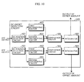
- Fig. 10 illustrates another example of the configuration of the DC offset detection circuit 103.
- the DC offset detection circuit 103 shown in Fig. 10 comprises a first circuit (a DC position detection circuit 401, a first differential circuit 402, a second differential circuit 403, a comparison circuit 404, and an integrator 405) for providing an offset amount to the one DC offset correction circuit 101, and a second circuit (a DC position detection circuit 501, a first differential circuit 502, a second differential circuit 503, a comparison circuit 504, and an integrator 505) for providing an offset amount to the other DC offset correction circuit 102.
- the DC position detection circuit 401 to which one of the signals outputted from the FFT circuit 9 is inputted, detects the level of a DC position.
- An output X of the DC position detection circuit 401 is + 1 + ⁇ or - 1 + ⁇ .
- the first differential circuit 402 subtracts - 1 from the output X of the DC position detection circuit 401 (adds + 1 thereto). An output value of the first differential circuit 402 is X + 1.
- the second differential circuit 403 subtracts + 1 from the output X of the DC position detection circuit 401. An output value of the second differential circuit 403 is X - 1.
- the comparison circuit 404 compares the output value (X + 1) of the first differential circuit 402 with the output value (X - 1) of the second differential circuit 403, and selects and outputs the smaller output value ⁇ .
- the integrator 405 integrates the output of the comparison circuit 404 for a predetermined time period, and outputs the results of the integration as an offset amount.
- the DC offset correction circuits 101 and 102 are provided in the succeeding stage of the FFT circuit 9
- the DC offset correction circuits 101 and 102 may be provided in the preceding stage of the FFT circuit 9, as illustrated in Fig. 11.
- correction is made before the FFT. Accordingly, the dynamic range of the FFT can be sufficiently made use of.
- a correction delay corresponding to a time period required for the FFT occurs.
- high-precision DC offset correction can be made in a simple configuration.
- Fig. 12 illustrates the configuration of a digital television receiver for performing partial receiving.
- Fig. 13 illustrates a spectrum in each of blocks shown in Fig. 12.
- a signal is transmitted by a spectrum as illustrated in Fig. 13 (a).
- Fig. 13 (a) a spectrum corresponding to UHF Channels 14 to 16 is illustrated.
- One channel has a band width of 6 HMz, and is composed of 13 segments. The segment at the center out of the 13 segments corresponds to a signal for partial receiving, by which partial receiving is possible. Description is made of a case where the UHF Channel 15 is partially received.
- Fig. 13 (b) is an enlarged view of the UHF Channel 15, which illustrates, taking a partial receiving object segment as S15-0 and taking segments in the lower and upper bands than the partial receiving object segment as S15-1 to S15-12, the segments S15-0 to S15-6.
- An RF signal corresponding to the UHF Channel 15 is frequency-converted into a Low IF signal by the down converter (the local signal generator 1, the mixers 2A and 3A, and the 90-degree phase shifter 4A) shown in Fig. 12.
- a signal having a frequency (for frequency-converting the RF signal such that the lower-end frequency of the occupied band of the partial receiving object segment S15-0 is in the vicinity of a frequency of zero) such that the partial receiving object segment S15-0 corresponds to the Low IF signal is outputted from the local signal generator 1A.
- a cosine signal and a sine signal are respectively outputted to the mixers 2A and 3A from the 90-degree phase shifter 4 so as to output a real axis component and an imaginary axis component.
- a spectrum after the frequency conversion by the down converter is as illustrated in Fig. 13 (c).
- the down converter frequency-converts the RF signal such that the lower-end frequency of the occupied band of the partial receiving object segment S15-0 is in the vicinity of a frequency of zero. Accordingly, the segment S15-1 whose component is folded back is multiplexed in a frequency band of the partial receiving object segment S15-0.
- the signals are transformed from time axis data to frequency axis data in an FFT circuit 9.
- the number of points of the FFT circuit 9 must be twice or more in order to separate signals corresponding to two segments.
- the segments in the UHF Channel 15 must have orthogonality. Accordingly, orthogonality is also maintained from the partial receiving object segment S15-0 and the segment S15-1. Therefore, a negative frequency component of the segment S15-1 and a positive frequency component of the partial receiving object segment S15-0 are completely separable from each other in the FFT circuit 9.
- a spectrum of outputs of the FFT circuit 9 is as illustrated in Fig. 13 (e).
- the segment 15-1 having a negative frequency component is removed from the outputs of the FFT circuit 9, respectively, by the unnecessary component removal circuits 10A and 11A, and obtained signals are outputted to a frequency de-interleave circuit 12. Consequently, a spectrum of the output signals of the unnecessary component removal circuits 10A and 11A is only the partial receiving object segment S15-0, as illustrated in Fig. 13 (f). Signal processing in the succeeding stage of the frequency de-interleave circuit 12 is the same as that in the receiver shown in Fig. 1.
- RF A*cos((wc+ ⁇ )t) + B*sin((wc+ ⁇ )t)) + C*cos((wc- ⁇ )t) + D*sin((wc- ⁇ )t))
- the signal is multiplied by cos(- ⁇ t) -jsin(- ⁇ t) and integrated for one period, to obtain A + jB, while being multiplied by cos( ⁇ t) - jsin( ⁇ t) and integrated for one period, to obtain C + jD. Accordingly, positive frequency components and negative frequency components can be completely separated from each other.
- the carriers in the partial receiving object segment S15-0 and the segment S15-1 are respectively defined as in the equations (4) and (5). Although the plus and minus signs of the frequency are reversed in the case of the FFT, therefore, this is not an essential problem.
- an analog IF filter generally realized by an SAW filter can be reduced, thereby making it possible to reduce the cost of the receiver.
Landscapes
- Engineering & Computer Science (AREA)
- Computer Networks & Wireless Communication (AREA)
- Signal Processing (AREA)
- Superheterodyne Receivers (AREA)
- Radar Systems Or Details Thereof (AREA)
- Monitoring And Testing Of Transmission In General (AREA)
Abstract
A direct conversion receiver comprises a down converter
for frequency-converting an analog RF signal modulated by an
OFDM method such that the center frequency of the occupied band
of a receiving object segment is a frequency of zero; AD
conversion means for converting a down converted signal
obtained by the down converter into a digital signal; FFT means
for subjecting the signal obtained by the AD conversion means
to fast Fourier transform, to transform the signal from time
axis data to frequency axis data; and unnecessary component
removal means for removing from an output signal of the FFT
means an unnecessary component other than the receiving object
segment.
Description
The present invention relates to a direct conversion
receiver, and more particularly, to a direct conversion
receiver that can be utilized for partial receiving for
receiving only one segment in terrestrial digital TV
broadcasting.
In recent years, in a system for transmitting a video
signal or an audio signal, an OFDM (Orthogonal Frequency
Division Multiplexing) method has been proposed as a method
superior in high-quality transmission and improvement in
frequency utilization efficiency.
The OFDM method is a modulation method for causing a lot
of sub-carriers to stand in a band including one channel. For
example, an analog TV signal is converted into a digital
signal, and the digital signal is then subjected to data
compression by MPEG (Moving Picture Expert Group). A data
signal thus obtained is subjected to byte interleaving and bit
interleaving so as to distribute the cause of errors in a
transmission path, for example, noises, and is subjected to
mapping corresponding to a modulation method such as QPSK
(Quadrature Phase Shift Keying) and 16 QAM (Quadrature
Amplitude Modulation).
Data obtained by the mapping is subjected to time
interleaving and frequency interleaving for dispersing the
cause of errors in a transmission path, for example, fading,
is then subjected to IFFT (inverse fast Fourier transform),
is subjected to orthogonal modulation, is then frequency-converted
into an RF frequency, and is transmitted.
Fig. 1 illustrates the configuration of a digital
television receiver.
In the digital television receiver, an operation
entirely reverse to that on the transmission side is
performed, to demodulate a TV signal.
An RF signal received by an antenna is inputted to a mixer
21. A signal corresponding to channel selection is also
inputted to the mixer 21 from a local signal generator 22, and
a signal obtained by frequency conversion is outputted such
that a desired frequency falls within a band of a BPF
(Band-Pass Filter) 23. In the BPF 23, only a desired frequency
component is extracted.
Outputs of the BPF 23 are respectively inputted to mixers
24 and 25. To the mixers 24 and 25, a cosine signal and a sine
signal are respectively inputted from a 90-degree phase
shifter 27 having as an input a signal from a local signal
generator 26. The mixers 24 and 25 respectively down-convert
the outputs of the BPF 23 which are IF (Intermediate Frequency)
signals, convert the down-converted outputs into Low IF
signals each comprising a real axis (I axis) component and an
imaginary axis (Q axis) component, and output the Low IF
signals to analog-to- digital converters 7 and 8.
In each of the analog-to- digital converters 7 and 8, an
analog signal (an I axis component and a Q axis component) is
converted into a digital signal, and the digital signal is
outputted to an FFT circuit 9. In the FFT circuit 9, the input
signal is subjected to fast Fourier transform (FFT), to
transform the signal from time axis data to frequency axis data
and output the signal to a frequency de-interleave circuit 12.
In the frequency de-interleave circuit 12, frequency
interleaving carried out in order to compensate for a signal
having a particular frequency which is missing due to the
reflection of electro-magnetic waves, for example, is
released. An output of the frequency de-interleave circuit
12 is fed to a time de-interleave circuit 13. The-time
de-interleave circuit 13 releases time interleaving carried
out for fading resistance or the like.
An I-axis and Q-axis signal obtained by the time deinterleaving
is fed to a de-mapping circuit 14, and is decoded
into 2 bits (QPSK), 4 bits (16 QAM), or 6 bits (64 QAM). A
signal obtained by de-mapping is fed to a bit de-interleave
circuit 15. The bit de-interleave circuit 15 releases bit
interleaving carried out for the purpose of increasing error
resistance. An output of the bit de-interleave circuit 15 is
fed to a Viterbi decoding circuit 16. The Viterbi decoding
circuit 16 makes error correction using a convolutional code
generated on the transmission side.
A signal obtained by Viterbi decoding is fed to a byte
de-interleave circuit 17. The byte de-interleave circuit 17
releases byte interleaving carried out for the purpose of
increasing error resistance, similarly to bit interleaving.
An output of the byte de-interleave circuit 17 is fed to an
RS decoding circuit 18. The RS decoding circuit 18 performs
RS (Reed-Solomon) decoding to make error correction. A signal
obtained by the error correction is fed to an MPEG decoding
circuit 19. The MPEG decoding circuit 19 extends a signal
obtained by the error correction (a compressed signal), and
outputs the extended signal to a digital-to-analog conversion
circuit 20. The digital-to-analog conversion circuit 20
converts the signal fed from the MPEG decoding circuit 19 into
an analog video/analog audio signal, and outputs the signal.
In a Japanese terrestrial digital broadcasting system,
a segment-divided signal format is employed. In the case of
television broadcasting, 13 segments are collectively
transmitted into a band of 6 MHz. Further, in the one segment
at the center out of the 13 segments, such partial receiving
that data broadcasting or the like can be performed by only
the one segment is possible. With respect to the receiving
of the 13 segments, the band width is only reduced to one-thirteenth
in the partial receiving, so that receiving is
possible in approximately the same configuration.
Fig. 2 illustrates a spectrum in each of the blocks shown
in Fig. 1 in a case where partial receiving is performed.
Fig. 2 (a) illustrates a spectrum of an RF (Radio
Frequency) signal corresponding to terrestrial digital
broadcasting (UHF). In Fig. 2 (a), a spectrum corresponding
to UHF Channels 14 to 16 is illustrated. One channel has a
band width of 6 HMz, and is composed of 13 segments. The
segment at the center out of the segments corresponds to a
signal for partial receiving.
Fig. 2 (b) illustrates a spectrum of the RF signal
corresponding to the UHF Channel 15, where the spectrum
corresponds to the six segments S15-0 to S15-6 at the center
out of the 13 segments.
Fig. 2 (c) illustrates a spectrum of an IF signal
corresponding to the UHF Channel 15 outputted from the mixer
21, where the spectrum corresponds to the six segments S15-0
to S15-6 at the center out of the 13 segments.
Fig. 2 (d) illustrates a spectrum of the IF signal
outputted from the BPF 23 in the case of partial receiving.
In the case of partial receiving, only the spectrum
corresponding to the one segment which is a partial receiving
object (hereinafter referred to as a partial receiving object
segment) S15-0 at the center in the spectrum of the IF signal
corresponding to the UHF Channel 15 is extracted by the BPF
23.
Fig. 2 (e) illustrates a spectrum of a Low IF signal
outputted from the mixer 24 or 25 at the time of partial
receiving.
Description was made of a so-called super heterodyne
system for converting an RF signal into an IF signal once and
then, converting the IF signal into a Low IF signal as a
receiving system. In a single carrier transmission system
such as QPSK modulation, a direct conversion system for
directly converting an RF signal into a base band signal is
also used as another receiving system. In the direct
conversion system, the necessity of components such as the
band-path filter 23 generally realized by an SAW (Surface
Acoustic Wave) filter is eliminated, thereby making it
possible to reduce the number of components.
Fig. 3 illustrates the configuration of a conventional
receiver using a direct conversion system. In Fig. 3, the same
blocks as those shown in Fig. 1 are assigned the same reference
numerals and hence, the description thereof is not repeated.
The difference between the conventional receiver using a
direct conversion system and the receiver using a super
heterodyne system shown in Fig. 1 is as follows:
Fig. 4 illustrates a spectrum in each of the units shown
in Fig. 3.
Fig. 4 (a) illustrates.a spectrum of an RF signal
corresponding to terrestrial digital broadcasting (UHF).
Fig. 4 (b) is an enlarged view of the UHF Channel 15,
which illustrates, taking a partial receiving object segment
as S15-0 and taking segments in the lower and upper bands than
the partial receiving object segment as S15-1 to S15-12, the
segments S15-0 to S15-6.
Fig. 4 (c) illustrates a spectrum after the frequency
conversion by the down converter (the local signal generator
1, the mixers 2 and 3, and the 90-degree phase shifter 4). The
down converter frequency-converts the RF signal such that the
center frequency of the occupied band of the partial receiving
object segment S15-0 is a frequency of zero (a DC component).
Accordingly, the RF signal is folded back at a frequency which
is one-half the occupied band of the partial receiving object
segment S15-0, and the folded signal is multiplexed.
Fig. 4 (d) illustrates a spectrum after removal of
frequency components (unnecessary components) higher than the
partial receiving object segment S15-0 by the LPFs 5 and 6.
Fig. 4 (e) illustrates a spectrum after transformation
from time axis data to frequency axis data in an FFT circuit
9, where only a signal corresponding to the partial receiving
object segment S15-0 is obtained.
In the conventional receiver using a direct conversion
system, the unnecessary components other than the partial
receiving object segment S15-0 are removed by the LPFs 5 and
6. Accordingly, an analog filter having steep characteristics
is required as the LPFs 5 and 6. An object of the present
invention is to provide a direct conversion receiver that
eliminates the necessity of using a steep analog filter so as
to remove an unnecessary component other than a receiving
object segment.
Another object of the present invention is to provide,
in a direct conversion receiver for frequency-converting an
RF signal such that the center frequency of the occupied band
is a frequency of zero (a DC component), a direct conversion
receiver in which high-precision DC offset correction is
possible in a simple configuration.
A further object of the present invention is to provide
a direct conversion receiver capable of reducing the circuit
scale.
A first direct conversion receiver according to the
present invention is characterized by comprising a down
converter for frequency-converting an analog RF signal
modulated by an OFDM method such that the center frequency of
the occupied band of a segment which is a receiving object
(hereinafter referred to as a receiving object segment) is a
frequency of zero; AD conversion means for converting a down
converted signal obtained by the down converter into a digital
signal; FFT means for subjecting the signal obtained by the
AD conversion means to fast Fourier transform, to transform
the signal from time axis data to frequency axis data; and
unnecessary component removal means for removing from an
output signal of the FFT means an unnecessary component other
than the receiving object segment.
A second direct conversion receiver according to the
present invention is characterized by comprising a down
converter for frequency-converting an analog RF signal
modulated by an OFDM method such that the center frequency of
the occupied band of a receiving object segment is a frequency
of zero; filter means for removing a high-frequency component
from a down converted signal obtained by the down converter;
AD conversion means for converting an output signal of the
filter means into a digital signal; FFT means for subjecting
the signal obtained by the AD conversion means to fast Fourier
transform; and unnecessary component removal means for
removing from an output signal of the FFT means an unnecessary
component other than the receiving object segment.
It is preferable that the above-mentioned first or
second direct conversion receiver is provided with DC offset
detection means for detecting a DC offset amount from a DC
component after the fast Fourier transform carried out by the
FFT means, and DC offset correction means for correcting DC
offset on the basis of the DC offset amount detected by the
DC offset detection means.
An example of the DC offset detection means is one for
integrating the DC component after the fast Fourier transform
carried out by the FFT means for a predetermined time period,
and taking an obtained integrated value as an offset amount.
An example of the DC offset detection means is one
comprising difference means having a plurality of reference
values and calculating and outputting a difference value
between the DC component after the fast Fourier transform
carried out by the FFT means and each of the reference values,
comparison means for selecting and outputting the minimum
value of the difference values calculated by the difference
means, and integration means for integrating the difference
value outputted by the comparison means for a predetermined
time period and outputting an obtained integrated value as an
offset amount.
A third direct conversion receiver according to the
present invention is characterized by comprising a down
converter for frequency-converting an analog RF signal
modulated by an OFDM method such that the upper-end frequency
or the lower-end frequency of the occupied band of a receiving
object segment is in the vicinity of a frequency of zero; AD
cohversion means for converting a down converted signal
obtained by the down converter into a digital signal; FFT means
for subjecting the signal obtained by the AD conversion means
to fast Fourier transform, to transform the signal from time
axis data to frequency axis data; and unnecessary component
removal means for removing from an output signal of the FFT
means an unnecessary component other than the receiving object
segment.
A fourth direct conversion receiver according to the
present invention is characterized by comprising a down
converter for frequency-converting an analog RF signal
modulated by an OFDM method such that the upper-end frequency
or the lower-end frequency of the occupied band of a receiving
object segment is in the vicinity of a frequency of zero;
filter means for removing a high-frequency component from a
down converted signal obtained by the down converter; AD
conversion means for converting an output signal of the filter
means into a digital signal; FFT means for subjecting the
signal obtained by the AD conversion means to fast Fourier
transform, to transform the signal from time axis data to
frequency axis data; and unnecessary component removal means
for removing from an output signal of the FFT means an
unnecessary component other than the receiving object
segment.
Referring now to Figs. 5 and 6, a first embodiment of
the present invention will be described.
Fig. 5 illustrates the configuration of a digital
television receiver for performing partial receiving. Fig.
6 illustrates a spectrum in each of blocks shown in Fig. 5.
In Fig. 5, the same blocks as those shown in Fig. 3 are
assigned same reference numerals and hence, the description
thereof is not repeated. The difference between the receiver
shown in Fig. 5 and the conventional example shown in Fig. 3
is as follows.
In Japanese terrestrial digital TV broadcasting, a
signal is transmitted by a spectrum as illustrated in Fig. 6
(a). In Fig. 6 (a), a spectrum corresponding to UHF Channels
14 to 16 is illustrated. One channel has a band width of 6
HMz, and is composed of 13 segments. The segment at the center
out of the 13 segments corresponds to a signal for partial
receiving, by which partial receiving is possible.
Description is made of a case where the UHF Channel 15 is
partially received.
Fig. 6 (b) is an enlarged view of the UHF Channel 15,
which illustrates, taking a segment which is a partial.
receiving object (hereinafter referred to as a partial
receiving object segment) as S15-0 and taking segments in the
lower and upper bands than the partial receiving object
segment as S15-1 to S15-12, the segments S15-0 to S15-6.
An RF signal corresponding to the UHF Channel 15 is
frequency-converted by a down converter (a local signal
generator 1, a 90-degree phase shifter 4, and mixers 2 and 3)
shown in Fig. 5. A signal having a frequency for
frequency-converting the RF signal is outputted from the local
signal generator 1 such that the center frequency of the
occupied band of the partial receiving object segment S15-0
becomes a frequency of zero. Further, a cosine signal and
a sine signal are respectively outputted to the mixers 2 and
3 from the 90-degree phase shifter 4 so as to output a real
axis component and an imaginary axis component.
A spectrum after the frequency conversion by the down
converter is as illustrated in Fig. 6 (c). The down converter
frequency-converts the RF signal such that the center
frequency of the occupied band of the partial receiving object
segment S15-0 becomes a frequency of zero (a DC component).
Accordingly, the RF signal is folded back at a frequency which
is one-half the occupied band of the partial receiving object
segment S15-0, and the folded signal is multiplexed.
Harmonic components of the signal are respectively
removed by the LPFs 5 and 6. A spectrum of output signals after
the removal of the harmonic components by the LPFs 5 and 6 is
as illustrated in Fig. 6 (d). An analog filter having gentler
characteristics, as compared with those in the conventional
example, is used as the LPFs 5 and 6. In the spectrum of the
output signals after the removal of the harmonic components
by the LPFs 5 and 6, therefore, not only the partial receiving
object segment S15-0 but also the segments S15-1 and S15-2
adjacent thereto remain.
The signals are transformed from time axis data to
frequency axis data in an FFT circuit 9. A spectrum of output
signals of the FFT circuit 9 is as illustrated in Fig. 6 (e).
The output signals of the FFT circuit 9 are outputted
to a frequency de-interleave circuit 12 after the segments
S15-1 to S15-2 which are unnecessary components other than the
partial receiving object segment S15-0 are respectively
removed therefrom in the unnecessary component removal
circuits 10 and 11. Consequently, a spectrum of the output
signals of the unnecessary component removal circuits 10 and
11 is only the partial receiving object segment S15-0, as
illustrated in Fig. 6 (f). Signal processing in the succeeding
stage of the frequency de-interleave circuit 12 is the same
as that in the receiver shown in Fig. 1.
For reference, the principle upon which folded signal
components of the partial receiving object segment S15-0 can
be separated by the FFT circuit 9 will be described.
For simplicity, if it is assumed that the center
frequency of the partial receiving object segment S15-0 is wc,
and carriers respectively exist in portions spaced ± α above
and below wc, a signal S0 corresponding to the segment S15-0
is expressed by the following equation (1):
S 0=A*cos((wc+α)t) + B*sin((wc-α)t))
Here, A to B denote the amplitudes of the signal.
The signal is multiplied by cos (wct) and sin (wct) so as
to convert a real axis component I and an imaginary axis
component Q of the RF signal into DCs, and its harmonic
components are then removed (a coefficient 1/2 is omitted),
the real axis component I is expressed'by the following
equation (2), and the imaginary axis component Q is expressed
by the following equation (3):
I=A*cos(αt) + B*sin(-αt)
Q=A*sin (-αt) + B*cos (αt)
In order to subject the signal to FFT, the signal is
multiplied by cos(-αt) -jsin(-αt) and integrated for one
period, to obtain A, while being multiplied by cos(αt) -
jsin(αt) and integrated for one period, to obtain B.
Accordingly, a positive frequency component and a negative
frequency component can be completely separated from each
other.
According to the above-mentioned first embodiment, the
necessity of using a steep analog filter so as to remove
unnecessary components other than the receiving object
segment is eliminated.
Referring now to Figs. 7 and 11, a second embodiment of
the present invention will be described.
Fig. 7 illustrates the configuration of a digital
television receiver using a direct conversion system. Fig.
8 illustrates a spectrum in each of blocks shown in Fig. 7.
In Fig. 7, the same blocks as those shown in Fig. 5 are
assigned same reference numerals and hence, the description
thereof is not repeated. The difference between the receiver
shown in Fig. 7 and the receiver shown in Fig. 5 is that DC
offset correction circuits 101 to 102 and a DC offset detection
circuit 103 are added.
In Japanese terrestrial digital TV broadcasting, a
signal is transmitted by a spectrum as illustrated in Fig. 8
(a). In Fig. 8 (a), a spectrum corresponding to UHF Channels
14 to 16 is illustrated. One channel has a band width of 6
HMz, and is composed of 13 segments. The segment at the center
out of the segments corresponds to a signal for partial
receiving. Description is made of a case where the UHF Channel
15 is partially received.
Fig. 8 (b) is an enlarged view of the UHF Channel 15,
which illustrates, taking a partial receiving object segment
as S15-0 and taking segments in the lower and upper bands than
the partial receiving object segment as S15-1 to S15-12, the
segments S15-0 to S15-6.
An RF signal corresponding to the UHF Channel 15 is
frequency-converted by a down converter (a local signal
generator 1, a 90-degree phase shifter 4, and mixers 2 and 3)
shown in Fig. 7. A signal having a frequency for
frequency-converting the RF signal is outputted from the local
signal generator 1 such that the center frequency of the
occupied band of the partial receiving object segment S15-0
becomes a frequency of zero. Further, a cosine signal and
a sine signal are respectively outputted to the mixers 2 and
3 from the 90-degree phase shifter 4 so as to output a real
axis component and an imaginary axis component.
A spectrum after the frequency conversion by the down
converter is as illustrated in Fig. 8 (c). The down converter
frequency-converts the RF signal such that the center
frequency of the occupied band of the partial receiving object
segment S15-0 is a frequency of zero (a DC component).
Accordingly, the RF signal is folded back at a frequency which
is one-half the occupied band of the partial receiving object
segment S15-0, and the folded signal is multiplexed.
Harmonic components of the signal are respectively
removed by the LPFs 5 and 6. A spectrum of output signals after
the removal of the harmonic components by the LPFs 5 and 6 is
as illustrated in Fig. 8 (d). An analog filter having
relatively gentle characteristics is used as the LPFs 5 and
6. In the spectrum of the output signals after the removal
of the harmonic components by the LPFs 5 and 6, therefore, not
only the partial receiving object segment S15-0 but also the
segments S15-1 and S15-2 adjacent thereto remain.
The signals are transformed from time axis data to
frequency axis data in an FFT circuit 9. A spectrum of output
signals of the FFT circuit 9 is as illustrated in Fig. 8 (e).
The output signals of the FFT circuit 9 are outputted
to a frequency de-interleave circuit 12 after the segments
S15-1 and S15-2 which are unnecessary components other than
the partial receiving object segment S15-0 are respectively
removed therefrom in the unnecessary component removal
circuits 10 and 11. Consequently, a spectrum of output signals
of the unnecessary component removal circuits 10 and 11 is only
the partial receiving object segment S15-0, as illustrated in
Fig. 8 (f). Signal processing in the succeeding stage of the
frequency de-interleave circuit 12 is the same as that in the
receiver shown in Fig. 1.
As in the spectrum shown in Fig. 8 (c), a DC component
(a component having a frequency of zero) is also a signal
component, so that a signal having no DC offset is required.
Examples of the cause of DC offset include DC offset of an
active element in a case where the mixers 2 and 3 and the LPFs
5 and 6 are active filters, analog-to- digital conversion
circuits 7 and 8, and so on.
In the receiver shown in Fig. 7, outputs after the FFT
in the FFT circuit 9 are inputted to the DC offset detection
circuit 103, and outputs of the DC offset detection circuit
103 are respectively inputted to the DC offset correction
circuits 101 and 102. In the DC offset correction circuits
101 and 102, a value at the time of DC output of the FFT circuit
9 is corrected depending on a DC offset amount in the DC offset
detection circuit 103.
Fig. 9 illustrates the configuration of the DC offset
detection circuit 103.
Generally, signal data are nearly randomized in
transmission signal processing. Therefore, a signal
component becomes a predetermined value when it is integrated
for a predetermined time period. The DC offset detection
circuit 103 utilizes the property, to integrate a DC component
of the output of the FFT circuit 9 for a predetermined time
period and take the results of the integration as a DC offset
amount.
The DC offset detection circuit 103 shown in Fig. 9
comprises a first circuit (a DC position detection circuit 201
and an integrator 202) for providing an offset amount to the
one DC offset correction circuit 101, and a second circuit (a
DC position detection circuit 301 and an integrator 302) for
providing an offset amount to the other DC offset correction
circuit 102.
The operations of both the circuits are the same and
hence, only the operation of the first circuit will be
described. The DC position detection circuit 201, to which
one of the signals outputted from the FFT circuit 9 is
inputted, detects the level of a DC position. The integrator
202 integrates the level of the DC position detected by the
DC position detection circuit 201 for a predetermined time
period, and outputs the results of the integration as an offset
amount.
Fig. 10 illustrates another example of the configuration
of the DC offset detection circuit 103.
When a signal component takes a value of + 1 or - 1,
outputs of the FFT circuit 9 are + 1 +α or - 1 + α, letting
α be the value of DC offset.
For example, when the output is + 1 +α, one is
respectively added and subtracted to and from the value, to
obtain 2 + α and α. The value, close to zero, out of the values,
i.e. , α is a DC offset amount. Similarly, when the output is
- 1 + α , one is respectively added and subtracted to and from
the value, to obtain α and - 2 +α . The value, close to zero,
out of the values, i.e. , α is a DC offset amount. A presumed
signal value is thus subtracted from the output of the FFT
circuit 9, to take, out of obtained values, the value close
to zero as a DC offset amount.
The DC offset detection circuit 103 shown in Fig. 10
comprises a first circuit (a DC position detection circuit
401, a first differential circuit 402, a second differential
circuit 403, a comparison circuit 404, and an integrator 405)
for providing an offset amount to the one DC offset correction
circuit 101, and a second circuit (a DC position detection
circuit 501, a first differential circuit 502, a second
differential circuit 503, a comparison circuit 504, and an
integrator 505) for providing an offset amount to the other
DC offset correction circuit 102.
The operations of both the circuits are the same and
hence, only the operation of the first circuit will be
described. The DC position detection circuit 401, to which
one of the signals outputted from the FFT circuit 9 is
inputted, detects the level of a DC position. An output X of
the DC position detection circuit 401 is + 1 +α or - 1 +α.
The first differential circuit 402 subtracts - 1 from
the output X of the DC position detection circuit 401 (adds
+ 1 thereto). An output value of the first differential
circuit 402 is X + 1. The second differential circuit 403
subtracts + 1 from the output X of the DC position detection
circuit 401. An output value of the second differential
circuit 403 is X - 1.
The comparison circuit 404 compares the output value (X
+ 1) of the first differential circuit 402 with the output
value (X - 1) of the second differential circuit 403, and
selects and outputs the smaller output value α. The
integrator 405 integrates the output of the comparison circuit
404 for a predetermined time period, and outputs the results
of the integration as an offset amount.
Although in the above-mentioned embodiment, the DC
offset correction circuits 101 and 102 are provided in the
succeeding stage of the FFT circuit 9, the DC offset correction
circuits 101 and 102 may be provided in the preceding stage
of the FFT circuit 9, as illustrated in Fig. 11. In a case
where the DC offset correction circuits 101 and 102 are
provided in the preceding stage of the FFT circuit 9,
correction is made before the FFT. Accordingly, the dynamic
range of the FFT can be sufficiently made use of. However,
a correction delay corresponding to a time period required for
the FFT occurs.
According to the present embodiment, high-precision DC
offset correction can be made in a simple configuration.
Referring now to Figs. 12 and 13, a third embodiment of
the present invention will be described.
Fig. 12 illustrates the configuration of a digital
television receiver for performing partial receiving. Fig.
13 illustrates a spectrum in each of blocks shown in Fig. 12.
In Fig. 12, the same blocks as those shown in Fig. 1 are
assigned same reference numerals and hence, the description
thereof is not repeated. The difference between the receiver
shown in Fig. 12 and the conventional example shown in Fig.
1 is as follows.
In Japanese terrestrial digital TV broadcasting, a
signal is transmitted by a spectrum as illustrated in Fig. 13
(a). In Fig. 13 (a), a spectrum corresponding to UHF Channels
14 to 16 is illustrated. One channel has a band width of 6
HMz, and is composed of 13 segments. The segment at the center
out of the 13 segments corresponds to a signal for partial
receiving, by which partial receiving is possible.
Description is made of a case where the UHF Channel 15 is
partially received.
Fig. 13 (b) is an enlarged view of the UHF Channel 15,
which illustrates, taking a partial receiving object segment
as S15-0 and taking segments in the lower and upper bands than
the partial receiving object segment as S15-1 to S15-12, the
segments S15-0 to S15-6.
An RF signal corresponding to the UHF Channel 15 is
frequency-converted into a Low IF signal by the down converter
(the local signal generator 1, the mixers 2A and 3A, and the
90-degree phase shifter 4A) shown in Fig. 12. A signal having
a frequency (for frequency-converting the RF signal such that
the lower-end frequency of the occupied band of the partial
receiving object segment S15-0 is in the vicinity of a
frequency of zero) such that the partial receiving object
segment S15-0 corresponds to the Low IF signal is outputted
from the local signal generator 1A. Further, a cosine signal
and a sine signal are respectively outputted to the mixers 2A
and 3A from the 90-degree phase shifter 4 so as to output a
real axis component and an imaginary axis component.
A spectrum after the frequency conversion by the down
converter is as illustrated in Fig. 13 (c). The down converter
frequency-converts the RF signal such that the lower-end
frequency of the occupied band of the partial receiving object
segment S15-0 is in the vicinity of a frequency of zero.
Accordingly, the segment S15-1 whose component is folded back
is multiplexed in a frequency band of the partial receiving
object segment S15-0.
Similarly, the segments S15-2 and S15-3 are overlapped
with each other, and the segments S15-4 and S15-5 are
overlapped with each other. Harmonic components of the signal
are respectively removed by the LPFs 5A and 6A. A spectrum
of output signals after the removal of the harmonic components
by the LPFs 5A and 6A is as illustrated in Fig. 13 (d).
The signals are transformed from time axis data to
frequency axis data in an FFT circuit 9. The number of points
of the FFT circuit 9 must be twice or more in order to separate
signals corresponding to two segments. Further, the segments
in the UHF Channel 15 must have orthogonality. Accordingly,
orthogonality is also maintained from the partial receiving
object segment S15-0 and the segment S15-1. Therefore, a
negative frequency component of the segment S15-1 and a
positive frequency component of the partial receiving object
segment S15-0 are completely separable from each other in the
FFT circuit 9. A spectrum of outputs of the FFT circuit 9 is
as illustrated in Fig. 13 (e).
The segment 15-1 having a negative frequency component
is removed from the outputs of the FFT circuit 9, respectively,
by the unnecessary component removal circuits 10A and 11A, and
obtained signals are outputted to a frequency de-interleave
circuit 12. Consequently, a spectrum of the output signals
of the unnecessary component removal circuits 10A and 11A is
only the partial receiving object segment S15-0, as
illustrated in Fig. 13 (f). Signal processing in the
succeeding stage of the frequency de-interleave circuit 12 is
the same as that in the receiver shown in Fig. 1.
For reference, the principle upon which the negative
frequency component can be detected by the FFT circuit 9 will
be described.
For simplicity, it is assumed that carriers respectively
exist in the partial receiving object segment S15-0 and the
segment S15-1, and signals respectively corresponding to the
segments are S0 and S1 expressed by the following equations
(4) and (5):
S 0=A*cos((wc+α)t) + B*sin((wc+α)t))
S 1=C*cos((wc-α)t) + D*sin((wc-α)t))
Let A to D be the amplitudes of the signals, and wc be
a frequency at the boundary between the partial receiving
object segment S15-0 and the segment S15-1. Consequently, the
RF signal is expressed by the following equation (6):
RF=A*cos((wc+α)t) + B*sin((wc+α)t))
+ C*cos((wc-α)t) + D*sin((wc-α)t))
The RF signal is multiplied by cos (wct) and sin (wct) so
as to convert the RF signal into a Low IF signal having a real
axis component I and an imaginary axis component Q, and its
harmonic components are then removed (a coefficient 1/2 is
omitted), the real axis component I is expressed by the
following equation (7) , and the imaginary axis component Q is
expressed by the following equation (8):
I=A*cos(αt) + B*sin(αt) + C*cos(-αt) + D*sin(-αt)
Q=A*sin(-αt) + B*cos(αt) + C*sin(αt) + D*cos(αt)
In order to subject the signal to FFT, the signal is
multiplied by cos(-αt) -jsin(-αt) and integrated for one
period, to obtain A + jB, while being multiplied by cos(α
t) - jsin(αt) and integrated for one period, to obtain C +
jD. Accordingly, positive frequency components and negative
frequency components can be completely separated from each
other.
In order to simplify the description, the carriers in
the partial receiving object segment S15-0 and the segment
S15-1 are respectively defined as in the equations (4) and (5).
Although the plus and minus signs of the frequency are reversed
in the case of the FFT, therefore, this is not an essential
problem.
According to the above-mentioned embodiment, an analog
IF filter generally realized by an SAW filter can be reduced,
thereby making it possible to reduce the cost of the receiver.
Claims (7)
- A direct conversion receiver characterized by comprising:a down converter for frequency-converting an analog RF signal modulated by an OFDM method such that the center frequency of the occupied band of a receiving object segment is a frequency of zero;AD conversion means for converting a down converted signal obtained by the down converter into a digital signal;FFT means for subjecting the signal obtained by the AD conversion means to fast Fourier transform, to transform the signal from time axis data to frequency axis data; andunnecessary component removal means for removing from an output signal of the FFT means an unnecessary component other than the receiving object segment.
- A direct conversion receiver characterized by comprising:a down converter for frequency-converting an analog RF signal modulated by an OFDM method such that the center frequency of the occupied band of a receiving object segment is a frequency of zero;filter means for removing a high-frequency component from a down converted signal obtained by the down converter;AD conversion means for converting an output signal of the filter means into a digital signal;FFT means for subjecting the signal obtained by the AD conversion means to fast Fourier transform; andunnecessary component removal means for removing from an output signal of the FFT means an unnecessary component other than the receiving object segment.
- The direct conversion receiver according to either one of claims 1 and 2, characterized by comprising DC offset detection means for detecting a DC offset amount from a DC component after the fast Fourier transform carried out by the FFT means, and DC offset correction means for correcting DC offset on the basis of the DC offset amount detected by the DC offset detection means.
- The direct conversion receiver according to claim 3, characterized in that the DC offset detection means integrates the DC component after the fast Fourier transform carried out by the FFT means for a predetermined time period, and takes an obtained integrated value as an offset amount.
- The direct conversion receiver according to claim 3, characterized in that the DC offset detection means comprises difference means having a plurality of reference values and calculating and outputting a difference value between the DC component after the fast Fourier transform carried out by the FFT means and each of the reference values, comparison means for selecting and outputting the minimum value of the difference values calculated by the difference means, and integration means for integrating the difference value outputted by the comparison means for a predetermined time period and outputting an obtained integrated value as an offset amount.
- A direct conversion receiver characterized by comprising:a down converter for frequency-converting an analog RF signal modulated by an OFDM method such that the upper-end frequency or the lower-end frequency of the occupied band of a receiving object segment is in the vicinity of a frequency of zero;AD conversion means for converting a down converted signal obtained by the down converter into a digital signal;FFT means for subjecting the signal obtained by the AD conversion means to fast Fourier transform, to transform the signal from time axis data to frequency axis data; andunnecessary component removal means for removing from an output signal of the FFT means an unnecessary component other than the receiving object segment.
- A direct conversion receiver characterized by comprising:a down converter for frequency-converting an analog RF signal modulated by an OFDM method such that the upper-end frequency or the lower-end frequency of the occupied band of a receiving object segment is in the vicinity of a frequency of zero;filter means for removing a high-frequency component from a down converted signal obtained by the down converter;AD conversion means for converting an output signal of the filter means into a digital signal;FFT means for subjecting the signal obtained by the AD conversion means to fast Fourier transform, to transform the signal from time axis data to frequency axis data; andunnecessary component removal means for removing from an output signal of the FFT means an unnecessary component other than the receiving object segment.
Applications Claiming Priority (7)
| Application Number | Priority Date | Filing Date | Title |
|---|---|---|---|
| JP2001332910A JP2003143101A (en) | 2001-10-30 | 2001-10-30 | Direct conversion receiver |
| JP2001332912 | 2001-10-30 | ||
| JP2001332910 | 2001-10-30 | ||
| JP2001332912A JP3696147B2 (en) | 2001-10-30 | 2001-10-30 | Direct conversion receiver |
| JP2001332911A JP3685750B2 (en) | 2001-10-30 | 2001-10-30 | OFDM demodulator |
| JP2001332911 | 2001-10-30 | ||
| PCT/JP2002/011119 WO2003039049A1 (en) | 2001-10-30 | 2002-10-25 | Direct conversion receiver |
Publications (2)
| Publication Number | Publication Date |
|---|---|
| EP1441457A1 true EP1441457A1 (en) | 2004-07-28 |
| EP1441457A4 EP1441457A4 (en) | 2010-10-20 |
Family
ID=27347754
Family Applications (1)
| Application Number | Title | Priority Date | Filing Date |
|---|---|---|---|
| EP02777966A Withdrawn EP1441457A4 (en) | 2001-10-30 | 2002-10-25 | Direct conversion receiver |
Country Status (4)
| Country | Link |
|---|---|
| US (1) | US20040240573A1 (en) |
| EP (1) | EP1441457A4 (en) |
| CN (1) | CN100550702C (en) |
| WO (1) | WO2003039049A1 (en) |
Families Citing this family (6)
| Publication number | Priority date | Publication date | Assignee | Title |
|---|---|---|---|---|
| US7215266B2 (en) * | 2004-05-21 | 2007-05-08 | Wionics Research | Hybrid DC offset cancellation scheme for wireless receiver |
| JP2010213107A (en) * | 2009-03-11 | 2010-09-24 | Fujitsu Semiconductor Ltd | Communication apparatus |
| JP5630648B2 (en) * | 2010-11-16 | 2014-11-26 | ソニー株式会社 | Reception device, reception method, and electronic device |
| US9183838B2 (en) * | 2013-10-09 | 2015-11-10 | Summit Semiconductor Llc | Digital audio transmitter and receiver |
| JP2020025400A (en) * | 2018-08-07 | 2020-02-13 | 株式会社東芝 | Wireless power transmission device and wireless power transmission method |
| US12255671B2 (en) * | 2023-03-16 | 2025-03-18 | International Business Machines Corporation | Separable, intelligible, single channel voice communication |
Family Cites Families (11)
| Publication number | Priority date | Publication date | Assignee | Title |
|---|---|---|---|---|
| JPH06326739A (en) * | 1993-05-11 | 1994-11-25 | Sharp Corp | Cofdm signal receiver |
| US5761190A (en) * | 1995-02-20 | 1998-06-02 | Pioneer Electronic Corporation | OFDM broadcast wave receiver |
| JPH1117644A (en) | 1997-06-27 | 1999-01-22 | Toshiba Corp | Radio base station, radio terminal, radio communication system and carrier allocation control method thereof |
| US7106689B1 (en) * | 1999-03-02 | 2006-09-12 | Matsushita Electric Industrial Co., Ltd. | OFDM transmission/reception apparatus |
| JP4284568B2 (en) * | 1999-03-18 | 2009-06-24 | ソニー株式会社 | Receiving apparatus and method, and recording medium |
| JP2001069112A (en) * | 1999-08-25 | 2001-03-16 | Sony Corp | OFDM transmitting apparatus, OFDM receiving apparatus, OFDM communication apparatus using them, and OFDM communication method |
| JP3799951B2 (en) * | 2000-04-13 | 2006-07-19 | ソニー株式会社 | OFDM transmission apparatus and method |
| US20030072393A1 (en) * | 2001-08-02 | 2003-04-17 | Jian Gu | Quadrature transceiver substantially free of adverse circuitry mismatch effects |
| GB0123290D0 (en) * | 2001-09-27 | 2001-11-21 | Nokia Corp | DC offset correction in a mobile communication system |
| US20030231726A1 (en) * | 2002-06-12 | 2003-12-18 | Andreas Schuchert | Arrangement and method for frequency domain compensation of OFDM signals with IQ imbalance |
| US7110734B2 (en) * | 2002-09-05 | 2006-09-19 | Maxim Integrated Products Inc. | DC offset cancellation in a zero if receiver |
-
2002
- 2002-10-25 US US10/491,625 patent/US20040240573A1/en not_active Abandoned
- 2002-10-25 WO PCT/JP2002/011119 patent/WO2003039049A1/en not_active Ceased
- 2002-10-25 EP EP02777966A patent/EP1441457A4/en not_active Withdrawn
- 2002-10-25 CN CNB028150929A patent/CN100550702C/en not_active Expired - Fee Related
Also Published As
| Publication number | Publication date |
|---|---|
| WO2003039049A9 (en) | 2010-10-14 |
| CN1537370A (en) | 2004-10-13 |
| US20040240573A1 (en) | 2004-12-02 |
| EP1441457A4 (en) | 2010-10-20 |
| CN100550702C (en) | 2009-10-14 |
| WO2003039049A1 (en) | 2003-05-08 |
Similar Documents
| Publication | Publication Date | Title |
|---|---|---|
| US7098967B2 (en) | Receiving apparatus | |
| EP1405479B1 (en) | Iq-imbalance | |
| US7443783B2 (en) | I/Q mismatch compensation in an OFDM receiver in presence of frequency offset | |
| CN1189001C (en) | Phase interpolation receiver for angle modulated RF signals | |
| US8224276B2 (en) | Method and arrangement for signal processing in a receiver that can be tuned to different carriers | |
| JP2004527187A (en) | Quadrature envelope sampling of intermediate frequency signals at the receiver | |
| CN1217100A (en) | Dual-mode radio receiver for receiving narrowband and wideband signals | |
| KR19980064403A (en) | Broadcast receiver | |
| JP2000013357A (en) | OFDM receiver | |
| EP1774739B1 (en) | Ofdm signal demodulator circuit and ofdm signal demodulating method | |
| US20040240573A1 (en) | Direct coversion receiver | |
| JPH11112462A (en) | Digital broadcast receiver | |
| JP4123320B2 (en) | Receiver and its IC | |
| JPH0779415A (en) | OFDM transmission method and transmitter / receiver thereof | |
| EP1045561A3 (en) | Frequency correction in multicarrier receivers | |
| JP3970058B2 (en) | Direct conversion receiver | |
| JP3685750B2 (en) | OFDM demodulator | |
| JP4214635B2 (en) | Digital radio equipment | |
| JP3696147B2 (en) | Direct conversion receiver | |
| JP3449164B2 (en) | Receiver | |
| JP4284568B2 (en) | Receiving apparatus and method, and recording medium | |
| JPH0974366A (en) | Direct conversion receiver | |
| JP3743417B2 (en) | Receiver | |
| JP2003143101A (en) | Direct conversion receiver | |
| GB2394373A (en) | A receiver for analog and digital signals which uses a digital signal processor for filtering |
Legal Events
| Date | Code | Title | Description |
|---|---|---|---|
| PUAI | Public reference made under article 153(3) epc to a published international application that has entered the european phase |
Free format text: ORIGINAL CODE: 0009012 |
|
| 17P | Request for examination filed |
Effective date: 20040405 |
|
| AK | Designated contracting states |
Kind code of ref document: A1 Designated state(s): AT BE CH CY DE DK ES FI FR GB GR IE IT LI LU MC NL PT SE TR |
|
| AX | Request for extension of the european patent |
Extension state: AL LT LV MK RO SI |
|
| A4 | Supplementary search report drawn up and despatched |
Effective date: 20100920 |
|
| 17Q | First examination report despatched |
Effective date: 20101217 |
|
| STAA | Information on the status of an ep patent application or granted ep patent |
Free format text: STATUS: THE APPLICATION HAS BEEN WITHDRAWN |
|
| 18W | Application withdrawn |
Effective date: 20110802 |