EP1440606B1 - Schichtenmodell für den entwurf einer mehrschichtigen leiterplatte - Google Patents
Schichtenmodell für den entwurf einer mehrschichtigen leiterplatte Download PDFInfo
- Publication number
- EP1440606B1 EP1440606B1 EP02776676A EP02776676A EP1440606B1 EP 1440606 B1 EP1440606 B1 EP 1440606B1 EP 02776676 A EP02776676 A EP 02776676A EP 02776676 A EP02776676 A EP 02776676A EP 1440606 B1 EP1440606 B1 EP 1440606B1
- Authority
- EP
- European Patent Office
- Prior art keywords
- modules
- layer
- model according
- printed circuit
- layer model
- Prior art date
- Legal status (The legal status is an assumption and is not a legal conclusion. Google has not performed a legal analysis and makes no representation as to the accuracy of the status listed.)
- Expired - Lifetime
Links
- 239000000463 material Substances 0.000 claims description 19
- 239000012780 transparent material Substances 0.000 claims description 4
- 238000001816 cooling Methods 0.000 claims description 2
- 238000004519 manufacturing process Methods 0.000 description 6
- 239000004020 conductor Substances 0.000 description 5
- 238000010276 construction Methods 0.000 description 4
- 238000013461 design Methods 0.000 description 4
- 238000011161 development Methods 0.000 description 3
- 230000018109 developmental process Effects 0.000 description 3
- 210000001331 nose Anatomy 0.000 description 3
- 238000007792 addition Methods 0.000 description 1
- 230000003466 anti-cipated effect Effects 0.000 description 1
- 238000013459 approach Methods 0.000 description 1
- 239000000969 carrier Substances 0.000 description 1
- 230000001419 dependent effect Effects 0.000 description 1
- 238000006073 displacement reaction Methods 0.000 description 1
- 238000005553 drilling Methods 0.000 description 1
- 238000005516 engineering process Methods 0.000 description 1
- 239000011521 glass Substances 0.000 description 1
- 239000000203 mixture Substances 0.000 description 1
- 238000012986 modification Methods 0.000 description 1
- 230000004048 modification Effects 0.000 description 1
- 230000003287 optical effect Effects 0.000 description 1
- 238000012552 review Methods 0.000 description 1
- 239000000758 substrate Substances 0.000 description 1
- 230000009469 supplementation Effects 0.000 description 1
- 238000012360 testing method Methods 0.000 description 1
- 238000012549 training Methods 0.000 description 1
Images







Classifications
-
- H—ELECTRICITY
- H05—ELECTRIC TECHNIQUES NOT OTHERWISE PROVIDED FOR
- H05K—PRINTED CIRCUITS; CASINGS OR CONSTRUCTIONAL DETAILS OF ELECTRIC APPARATUS; MANUFACTURE OF ASSEMBLAGES OF ELECTRICAL COMPONENTS
- H05K3/00—Apparatus or processes for manufacturing printed circuits
-
- H—ELECTRICITY
- H05—ELECTRIC TECHNIQUES NOT OTHERWISE PROVIDED FOR
- H05K—PRINTED CIRCUITS; CASINGS OR CONSTRUCTIONAL DETAILS OF ELECTRIC APPARATUS; MANUFACTURE OF ASSEMBLAGES OF ELECTRICAL COMPONENTS
- H05K3/00—Apparatus or processes for manufacturing printed circuits
- H05K3/46—Manufacturing multilayer circuits
- H05K3/4611—Manufacturing multilayer circuits by laminating two or more circuit boards
Definitions
- the invention relates to a layer model for the design of a multilayer printed circuit board according to the preamble of claim 1.
- Multilayer printed circuit boards are used for the realization of electronic circuits with highly integrated circuits.
- a large number of technical requirements must be met.
- circuit designers to present concepts for the implementation of electronic circuits to a PCB manufacturer, and the PCB manufacturer has reviewed these concepts for technical feasibility.
- a considerable exchange of information was necessary to finally create a technically feasible concept.
- the invention has for its object to provide a layered model that allows on the basis of the available materials and mechanical and technical parameters, a preliminary check of the feasibility of an electronic circuit on a multilayer printed circuit board at an early stage of the design of such a circuit board.
- the construction of a multilayer printed circuit board of individual components can be carried out in the form of a modular system, which can be assembled by exchange, displacement, removal or supplementation to form a valid and feasible layer model for a printed circuit board.
- the circuit designer can thus create, modify and check the technical feasibility. This makes it possible to achieve a result that is either already implemented as a finished concept or requires only minor modifications by the PCB manufacturer.
- the layer modules comprise at least base material modules of the printed circuit board, insulating layer modules and printed conductor modules.
- modules it is already possible to simulate the layer structure of a multilayer printed circuit board and to specify it as a concept.
- different modules can be combined individually in a simple manner in order to empirically create a concept for the production of a printed circuit board, taking into account the feasibility.
- the layer modules can additionally combination modules of combined base material modules and / or insulating layers modules and / or interconnect modules and / or impedance modules and / or decoupling modules and / or capacity modules and / or stiffening modules and / or cooling modules.
- the layer modules and the contacting modules and bore modules based on the layer thickness of the multilayer printed circuit board to scale and executed on an enlarged scale.
- the corresponding modules can thus be combined without optical aids, since they correspond exactly to the later thickness ratios of the multilayer printed circuit board on an enlarged scale.
- the layer modules and the contacting modules and bore modules are present multiple times and in the customary thickness and length graduations.
- the layer modules as well as the contacting modules and bore modules can carry symbols and labels.
- the mounting frame can also carry labels.
- the material used is a non-transparent material and the labels are arranged on both sides.
- the material used is a transparent material and the labels are arranged on one side.
- additional information cards made of the same material as the mounting frame and the modules can be provided with instructions for the user.
- the corresponding instructions for the user can thus be displayed on the same medium, and thus the same advantages can be used that also apply to the layer modules and the mounting frame.
- Fig. 1 shows a mounting frame with inserted layers modules and placed contacting and bore modules.
- the mounting frame has approx. A4 format.
- the middle area of the frame contains a window into which the individual modules for the construction of the multilayer printed circuit board can be inserted.
- a scale to the left and right of the window indicates the anticipated final thickness of the multilayer printed circuit board that will be after pressing and surface finishing.
- the contour of the window in the mounting frame has a recess on the upper and lower side left and right. This recess has the function of a coding and allows a flush application to the frame only of those layer modules that should complete a multilayer structure of the circuit board.
- the layer modules inserted in the frame can be moved up and down. This makes additions or exchanges easy and uncomplicated possible.
- the modules that can be used include all the components required in printed circuit board technology for the construction of multilayer printed circuit boards.
- the layer modules are basic material modules, insulating layer modules and printed circuit board modules.
- combination modules which are formed from base material, insulating layers and conductor tracks as a laminate. Combinations of base material and interconnects or insulating layers and interconnects are possible.
- the interconnect levels always have a coding nose, which in a CodierausEnglishung fits at the top or bottom of the window in the mounting frame.
- Combination modules from the combination of an insulating layer with a conductor layer layer can be covered on both sides with conductor tracks or on one side. When used on both sides, the combination modules have a coding nose at the top and bottom, and at one side only at the printed circuit board level. Such standard combinations must always be combined as a pair.
- Contacting modules and bore modules are placed on the layer modules used in the mounting frame. Contacting modules illustrate the possibility of a via and hole symbols the possibility of a blind hole. For the length of the contacting modules and bore modules, manufacturing limitations for the galvanic contacting, which result from the depth-width ratio of the bore, have been taken into account. If a contacting module or hole module can be laid out in such a way that the interconnect areas to be galvanically interconnected are covered, galvanic contacting is possible, otherwise it is not possible.
- the layer modules as well as the contacting modules and bore modules are executed on a scale of 100: 1, and the inscription on the edge of the mounting frame is also executed on this scale.
- the layer modules are subdivided into three fields which are labeled or provided with symbols. In the middle is the symbol for the type of material, on the left the naming of the material with a size specification and on the right the type of trace, possibly supplemented by electrical data.
- the symbol and an indication of the type of module and the length-diameter ratio is used.
- FIG. 2 shows an illustration of the mounting frame without inserted layer modules.
- information cards are inserted in the window of the mounting frame.
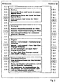
- FIGS. 3 to 6 show representations of different layer modules, specifically in FIGS. 3 and 4 base material modules, in FIG. 5 insulating layer modules, and in FIG. 6 printed circuit board modules in customary thickness graduations.
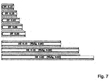
- Fig. 7 show above representations of different bore modules and and below representations of different contacting modules.
- the individual modules have customary thickness and length graduations.
- the modules shown in Figures 3 to 6 are also present at the same thickness multiple times and the modules shown in Fig. 7, even with the same thickness or length multiple times to create appropriate combinations of similar modules.
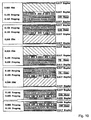
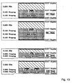
- FIGS. 8 to 13 show illustrations of different combination modules.
- the combination modules are These are modules that show a combined layer structure that can be implemented in practice. Based on the know-how of the printed circuit board manufacturer, results for the electrical properties of these combination modules were found, which are already entered in the fields of the combination modules. These allow the circuit designer to obtain the electrical properties without any calculations of their own, based solely on the choice of suitable layer modules.
- the layer modules With the help of the layer modules, it is thus possible to simulate the layer structure of a multilayer printed circuit board for the realization of an electronic circuit and to check in advance for feasibility.
- the illustrated modules are only part of the selection options. Although they are matched in the specific design of the current manufacturing capabilities of a particular PCB manufacturer, the design can be but without the inventive principle to rely on other manufacturing options adapt or update. These adjustments mainly relate to thickness gradations, the combination options for combination modules and the electrical specifications for combination modules.
- All modules have information on the strip width, the ohm value, the strip thickness and the laminate and insulating layer distances.
Landscapes
- Engineering & Computer Science (AREA)
- Manufacturing & Machinery (AREA)
- Microelectronics & Electronic Packaging (AREA)
- Structure Of Printed Boards (AREA)
- Production Of Multi-Layered Print Wiring Board (AREA)
- Supporting Of Heads In Record-Carrier Devices (AREA)
- Fixed Capacitors And Capacitor Manufacturing Machines (AREA)
- Laminated Bodies (AREA)
Description
- Die Erfindung betrifft ein Schichtenmodell für den Entwurf einer mehrschichtigen Leiterplatte nach dem Oberbegriff des Anspruchs 1.
- Mehrschichtige Leiterplatten werden zur Realisierung elektronischer Schaltungen mit hochintegrierten Schaltkreisen verwendet. Beim Entwurf mehrschichtiger Leiterplatten müssen eine Vielzahl technischer Anforderungen erfüllt werden. Bisher war es üblich, dass Schaltungsentwickler einem Leiterplattenhersteller Konzepte für die Umsetzung der elektronischen Schaltungen vorlegten und der Leiterplättenhersteller diese Konzepte auf technische Machbarkeit überprüfte. Besonders bei komplexen Aufbauten war ein erheblicher Informationsaustausch nötig, um schließlich ein technisch durchführbares Konzept zu erstellen.
- Die bisherige Vorgehensweise könnte vereinfacht werden, wenn dem Schaltungsentwickler zusätzliche Informations- und Testmöglichkeiten zur Verfügung stehen, um vorab das Konzept auf technische Machbarkeit hinsichtlich der Leiterplattenfertigung überprüfen zu können. Dazu sind allerdings disziplinübergreifende Informationen für den Schaltungsentwickler nötig, die einfach anwendbar und umsetzbar sind.
- Der Erfindung liegt die Aufgabe zugrunde, ein Schichtenmodell zu schaffen, das auf der Basis der verfügbaren Materialien und mechanischen und technischen Parameter eine Vorabprüfung der Umsetzbarkeit einer elektronischen Schaltung auf eine mehrschichtige Leiterplatte bereits in einem frühen Stadium des Entwurfs einer solchen Leiterplatte ermöglicht.
- Diese Aufgabe wird bei einem Schichtenmodell gemäß dem Anspruch 1 gelöst.
- Weiterbildungen und vorteilhafte Ausgestaltungen ergeben sich aus den Unteransprüchen.
- Mit dem erfindungsgemäßen Schichtenmodell kann in Form eines Baukastens die Konstruktion einer mehrschichtigen'Leiterplatte aus einzelnen Komponenten durchgeführt werden, die sich durch Austausch, Verschieben, Entfernen oder Ergänzen zu einem gültigen und machbaren Schichtenmodell für eine Leiterplatte zusammensetzen lassen. Der Schaltungsentwickler kann so das ihm vorschwebende Konzept erstellen, verändern und auf die technische Machbarkeit überprüfen. Dadurch gelingt es, ein Ergebnis zu erzielen, das entweder bereits als fertiges Konzept umsetzbar ist oder nur noch geringer Modifikationen seitens des Leiterplattenherstellers bedarf.
- Gemäß einer Weiterbildung ist vorgesehen, dass die Schichtenmodule wenigstens Basismaterial-Module der Leiterplatte, Isolierschichten-Module und Leiterbahn-Module umfassen.
- Mit Hilfe dieser Module ist es bereits möglich, den Schichtaufbau einer mehrschichtigen Leiterplatte zu simulieren und als Konzept vorzugeben. Dabei können in einfacher Weise unterschiedliche Module einzeln kombiniert werden, um empirisch unter Berücksichtigung der Machbarkeit ein Konzept für die Herstellung einer Leiterplatte zu erstellen.
- Ergänzend können die Schichtenmodule zusätzlich Kombinations-Module aus miteinander kombinierten Basismaterial-Modulen und/oder Isolierschichten-Modulen und/oder Leiterbahn-Modulen und/oder Impedanz-Modulen und/oder Entkopplungs-Modulen und/oder Kapazitäts-Modulen und/oder Versteifungs-Modulen und/oder Kühlungs-Modulen umfassen.
- Mit Hilfe der Kombinations-Module lassen sich bereits vorberechnete Kombinationen realisieren, die auf bestimmte physikalische Anforderungen abgestimmt sind. Dem Schaltungsentwickler ist es dadurch möglich, Kenntnisse aus einer anderen Disziplin, nämlich der Leiterplattenherstellung ohne eigene tiefer gehende Kenntnisse und Berechnungen übernehmen zu können und hiermit ein funktionsfähiges Konzept zu erstellen. Für den Schaltungsentwickler wird damit sinngemäß das Know-How des Leiterplattenherstellers verfügbar gemacht, ohne dass er sich hierbei um Einzelheiten und die Zusammenhänge kümmern muss.
- Ferner sind Kontaktierungs-Module und/oder Bohrungs-Module zum Auflegen oder Anlegen an die Schichten-Module vorgesehen. Hierdurch ist es möglich, Kontaktierungswünsche zwischen unterschiedlichen Leiterbahn-Schichten auszuprobieren und auszulegen.
- Vorzugsweise weisen der Montagerahmen und wenigstens ein Teil der Schichtenmodule Codierungsnasen und/oder Codierungsausnehmungen auf, die beim bündigen Aneinandersetzen ineinander greifen.
- Durch diese Maßnahmen wird erreicht, dass Fehler bei der Zusammenstellung der einzelnen Module sofort erkennbar werden, wenn die Codierungsnasen und/oder Codierungsaizsnehmungen nicht ineinander passen. Hingegen bieten Kombinationen von Schichtenmodulen mit passenden Codierungsnasen und/oder Codierungsausnehmungen die Gewähr, dass derartige Kombinationen auch technisch realisierbar sind.
- Bei einer Weiterbildung sind die Schichten-Module sowie die Kontaktierungs-Module und Bohrungs-Module bezogen auf die Schichtdicke der mehrschichtigen Leiterplatte maßstabsgetreu und in einem vergrößerten Maßstab ausgeführt.
- Die entsprechenden Module lassen sich so ohne optische Hilfsmittel kombinieren, da sie im vergrößerten Maßstab exakt den späteren Dickenverhältnissen der mehrschichtigen Leiterplatte entsprechen.
- Weiterhin ist vorgesehen, dass die Schichten-Module sowie die Kontaktierungs-Module und Bohrungs-Module mehrfach und in den anwendungsüblichen Dicken- und Längenabstufungen vorhanden sind.
- Dadurch lassen sich alle anwendungsüblichen Kombinationen hinsichtlich der Materialien und Schichtdicken simulieren und so ein für die spezifische Anwendung machbarer Aufbau erzeugen.
- Ferner können die Schichten-Module sowie die Kontaktierungs-Module und Bohrungs-Module Symbole und Beschriftungen tragen.
- Diese erleichtern dem Schaltungsentwickler den Aufbau eines Modells allein aufgrund der Informationsträger auf den Modulen selbst und erspart somit die sonst nötige zusätzlich Heranziehung von externen Informationen oder Handbüchern.
- Darüber hinaus kann auch der Montagerahmen Beschriftungen tragen.
- Diese ermöglichen z. B. eine einfache Überprüfung der gesamten Schichtdicke, ohne dass die Schichtdicken der einzelnen Module addiert werden müssten.
- Gemäß einer Weiterbildung ist vorgesehen, dass als Material ein nicht-transparenter Werkstoff dient und die Beschriftungen doppelseitig angeordnet sind.
- Bei dieser Ausgestaltung ist es möglich, einerseits das Schichtenmodell von oben zu betrachten, andererseits aber auch auf einer Unterlage zusammengebaut mit der dann gleichartigen Unterseite auf die Glasplatte eines Scanners oder Kopiergerätes zu schieben oder zusammen mit der in diesem Fall transparenten Unterlage zu legen und den Schichtenaufbau mit Übernahme der entsprechenden Symbole und Beschriftungen zu kopieren. Es besteht hier nicht die Gefahr, dass bei dem sonst nötigen Wendevorgang einzelne Module aus dem Montagerahmen herausfallen und falsch zusammengesetzt werden könnten.
- Gemäß einer Alternative ist vorgesehen, dass als Material ein transparenter Werkstoff dient und die Beschriftungen einseitig angeordnet sind.
- Hierdurch ist es möglich, das Schichtenmodell im Rahmen einer Schulung auch auf einen overhead-Projektor zu legen und über Durchlicht-Projektion darzustellen.
- Ergänzend können zusätzlich Informationskarten aus dem gleichen Werkstoff wie der Montagerahmen und die Module mit Hinweisen für den Anwender vorgesehen sein.
- Die entsprechenden Hinweise für den Anwender lassen sich auf diese Weise auf dem gleichen Medium darstellen, und somit lassen sich die gleichen Vorteile nutzen die auch für die Schichten-Module und den Montagerahmen gelten.
- Nachfolgend wird die Erfindung anhand eines Ausführungsbeispiels erläutert, das in der Zeichnung dargestellt ist.
- In der Zeichnung zeigen:
- Fig. 1
- einen Montagerahmen mit eingelegten Schichten-Modulen und aufgelegten Kontaktierungs- und Bohrungs-Modulen,
- Fig. 2
- einen Montagerahmen mit Informations-Modulen,
- Fig. 3, 4
- eine Darstellung unterschiedlicher Schichten-Module als Basismaterial-Module,
- Fig. 5
- eine Darstellung unterschiedlicher Schichten-Module als Isolierschichten-Module,
- Fig. 6
- eine Darstellung unterschiedlicher Schichten-Module als Leiterbahn-Module,
- Fig. 7
- eine Darstellung unterschiedlicher Bohrungs-Module und Kontaktierungs-Module,
- Fig. 8 - 13
- eine Darstellung unterschiedlicher Kombinations-Module.
- Fig. 1 zeigt einen Montagerahmen mit eingelegten Schichten-Modulen und aufgelegten Kontaktierungs- und Bohrungs-Modulen. Der Montagerahmen hat ca. das Format A4. Der mittlere Bereich des Rahmens enthält ein Fenster, in das die einzelnen Module für den Aufbau der mehrschichtigen Leiterplatte eingelegt werden können.
- Eine Skala links und rechts des Fensters zeigt die voraussichtliche Enddicke der mehrschichtigen Leiterplatte an, die diese nach dem Verpressen und der Oberflächenbearbeitung haben wird. Die Kontur des Fensters im Montagerahmens weist an der oberen und unteren Seite links und rechts eine Ausnehmung auf. Diese Ausnehmung hat die Funktion einer Codierung und ermöglicht ein bündiges Anlegen an den Rahmen nur von solchen Schichten-Modulen, die einen mehrschichtigen Aufbau der Leiterplatte abschließen sollten. Die im Rahmen eingelegten Schichtenmodule können hoch und runter verschoben werden. Dadurch sind Ergänzungen oder der Austausch einfach und unkompliziert möglich.
- Zu den einsetzbaren Modulen gehören alle Komponenten, die in der Leiterplattentechnik für den Aufbau von mehrschichtigen Leiterplatten erforderlich sind. Bei den Schichtenmodulen handelt es sich in einer Basisausführung um Basismaterial-Module, Isolierschicht-Module und Leiterbahn-Module. Darüber hinaus sind auch Kombinations-Module vorhanden, die aus Basismaterial, Isolierschichten und Leiterbahnen als Laminat gebildet sind. Auch Kombinationen aus Basismaterial und Leiterbahnen oder Isolierschichten und Leiterbahnen sind möglich.
- Für den Aufbau einer mehrschichtigen Leiterplatte gilt allgemein die Regel, dass die oberste und unterste Schicht jeweils mit einer Leiterbahn abgeschlossen sein soll. Daher weisen die Leiterbahnebenen stets eine Codiernase auf, die in eine Codierausnehmung am oberen oder unteren Ende des Fensters im Montagerahmen hineinpasst.
- Kombinations-Module aus der Kombination einer Isolierschicht mit einer Leiterbahnschicht können beidseitig mit Leiterbahnen oder einseitig belegt sein. Bei beidseitiger Belegung weisen die Kombinations-Module oben und unten eine Codiernase auf, bei einseitig belegten nur an der Leiterbahnebene. Derartige Standartkombinationen müssen immer als Paar zusammengefasst werden.
- Auf die in den Montagerahmen eingesetzten Schichten-Module sind Kontaktierungs-Module und Bohrungs-Module aufgelegt. Kontaktierungs-Module veranschaulichen die Möglichkeit einer Durchkontaktierung und Bohrungssymbole die Möglichkeit einer Blindbohrung. Für die Länge der Kontaktierungs-Modüle und Bohrungs-Module wurden fertigungstechnische Einschränkungen für das galvanische Kontaktieren berücksichtigt, die sich aus dem Tiefen-Breiten-Verhältnis der Bohrung ergeben. Lässt sich ein Kontaktierungs-Modul oder Bohrungs-Modul so anlegen, dass die galvanisch miteinander zu verbindenden Leiterbahnflächen überdeckt werden, dann ist ein galvanisches Kontaktieren möglich, anderenfalls ist es nicht möglich.
- Die Schichtenmodule sowie die Kontaktierungs-Module und Bohrungs-Module sind im Maßstab 100 : 1 ausgeführt, und in diesem Maßstab ist auch die Beschriftung am Rande des Montagerahmens ausgeführt. Die Schichten-Module sind in drei Felder unterteilt, die beschriftet oder mit Symbolen versehen sind. In der Mitte ist jeweils das Symbol für die Art des Materials, links die Benennung des Materials mit einer Größenangabe und rechts die Art der Leiterbahn, eventuell ergänzt durch elektrische Angaben.
- Bei den Kontaktierungs-Modulen und Bohrungs-Modulen ist das Symbol sowie eine Angabe zur Art des Moduls und zum Längen-Durchmesser-Verhältnis eingesetzt.
- Fig. 2 zeigt eine Darstellung des Montagerahmens ohne eingesetzte Schichten-Module. Zusätzlich sind in das Fenster des Montagerahmens Informationskarten eingelegt.
- Die Figuren 3 bis 6 zeigen Darstellungen unterschiedlicher Schichten-Module, und zwar in Fig. 3 und 4 Basismaterial-Module, in Fig. 5 Isolierschichten-Module und in Fig. 6 Leiterbahn-Modüle in anwendungsüblichen Dickenabstufungen.
- Fig. 7 zeigen oben Darstellungen unterschiedlicher Bohrungs-Module und und unten Darstellungen unterschiedlicher Kontaktierungs-Module. Die einzelnen Module weisen anwendungsübliche Dicken- und Längenabstufungen auf.
- In einem Baukastensystem sind die in den Figuren 3 bis 6 dargestellten Module auch bei gleicher Dicke mehrfach vorhanden und die in Fig. 7 dargestellten Module auch bei gleicher Dicke oder Länge mehrfach vorhanden, um entsprechende Kombinationsmöglichkeiten gleichartiger Module zu schaffen.
- Die Figuren 8 bis 13 zeigen Darstellungen unterschiedlicher Kombinations-Module. Bei den Kombinations-Modulen handelt es sich um Module, die einen kombinierten Schichtenaufbau, der anwendungsmäßig realisierbar ist, zeigen. Aufgrund des Know-Hows des Leiterplattenherstellers wurden Ergebnisse für die elektrischen Eigenschaften dieser Kombinations-Module ermittelt, die bereits in den Feldern der Kombinations-Module eingetragen sind. Diese ermöglichen es dem Schaltungsentwickler, die elektrischen Eigenschaften ohne eigene Berechnungen allein aufgrund der Auswahl der geeigneten Schichten-Module zu erlangen.
- Mit Hilfe der Schichtenmodule ist es somit möglich, den Schichtenaufbau einer mehrschichtigen Leiterplatte zur Realisierung einer elektronischen Schaltung zu simulieren und vorab auf Machbarkeit zu überprüfen. Die dargestellten Module stellen hierbei nur einen Teil der Auswahlmöglichkeiten.dar. Sie sind zwar in der konkreten Ausgestaltung auf die aktuellen Fertigungsmöglichkeiten eines bestimmten Leiterplattenherstellers abgestimmt, die Ausgestaltung lässt sich aber ohne das erfindungsgemäße Prinzip zu verlassen an andere Fertigungsmöglichkeiten anpassen oder aktualisieren. Diese Anpassungen betreffen im wesentlichen Dickenabstufungen, die Kombinationsmöglichkeiten bei Kombinations-Modulen und die elektrischen Angaben bei Kombinations-Modulen.
- Alle Module weisen Angaben der Leiterbahnbreite, des Ohm-Wertes, der Leiterbahndicke und der Laminat- sowie Isolierschichtabstände auf.
Claims (12)
- Schichtenmodell für den Entwurf einer mehrschichtigen Leiterplatte, bestehend aus einem Montagerahmen und einer Vielzahl Schichtenmodule, die zur Simulation des Schichtenaufbaus der mehrschichtigen Leiterplatte bündig aneinsetzbar und in den Montagerahmen einsetzbar sind.
- Schichtenmodell nach Anspruch 1, dadurch gekennzeichnet, dass die Schichtenmodule wenigstens Basismaterial-Module der Leiterplatte, Isolierschichten-Module und Leiterbahh-Module umfassen.
- Schichtenmodell nach Anspruch-2, dadurch gekennzeichnet, dass die Schichtenmodule zusätzlich Kombinations-Module aus' miteinander kombinierten Basismaterial-Modulen und/oder Isolierschichten-Modulen und/oder Leiterbahn-Modulen und/oder Impedanz-Modulen und/oder Entkopplungs-Modulen und/oder Kapazitäts-Modulen und/oder Versteifungs-Modulen und/oder Kühlungs-Modulen umfassen.
- Schichtenmodell nach einem der Ansprüche 1 bis 2, dadurch gekennzeichnet, dass zusätzlich Kontaktierungs-Module und/oder Bohrungs-Module zum Auflegen oder Anlegen an die Schichtenmodule vorgesehen sind.
- Schichtenmodell nach einem der Ansprüche 1 bis 4, dadurch gekennzeichnet, dass der Montagerahmen und wenigstens ein Teil der Schichtenmodule Codierungsnasen und/oder Codierungsausnehmungen aufweist, die beim bündigen Aneinandersetzen ineinander greifen.
- Schichtenmodell nach einem der Ansprüche 1 bis 5, dadurch gekennzeichnet, dass die Schichtenmodule sowie die Kontaktierungs-Module und Bohrungs-Module bezogen auf die Schichtdicke der mehrschichtigen Leiterplatte maßstabsgetreu in einem vergrößerten Maßstab ausgeführt sind.
- Schichtenmodell nach einem der Ansprüche 1 bis 6, dadurch gekennzeichnet, dass die Schichtenmodule sowie die Kontaktierungs-Module und Bohrungs-Module mehrfach und in den praxisüblichen Dicken- und Längenabstufungen vorhanden sind.
- Schichtenmodell nach einem der Ansprüche 1 bis 7, dadurch gekennzeichnet, dass die Schichtenmodule sowie die Kontaktierungs-Module und Bohrungs-Module Symbole und Beschriftungen tragen.
- Schichtenmodell nach einem der Ansprüche 1 bis 8, dadurch gekennzeichnet, dass der Montagerahmen Beschriftungen trägt.
- Schichtenmodell nach Anspruch 8 oder 9, dadurch gekennzeichnet, dass als Material ein nicht-transparenter Werkstoff dient und die Beschriftungen doppelseitig angeordnet sind.
- Schichtenmodell nach Anspruch 8 oder 9, dadurch gekennzeichnet, dass als Material ein transparenter Werkstoff dient und die Beschriftungen einseitig angeordnet sind.
- Schichtenmodell nach Anspruch 10 oder 11, dadurch gekennzeichnet, dass zusätzlich Informationskarten aus dem gleichen Werkstoff mit Hinweisen für den Anwender vorgesehen sind.
Applications Claiming Priority (5)
| Application Number | Priority Date | Filing Date | Title |
|---|---|---|---|
| DE20117912U DE20117912U1 (de) | 2001-11-02 | 2001-11-02 | Schichtenmodell für den Entwurf einer mehrschichtigen Leiterplatte |
| DE2001154087 DE10154087C2 (de) | 2001-11-02 | 2001-11-02 | Schichtenmodell für den Entwurf einer mehrschichtigen Leiterplatte |
| DE10154087 | 2001-11-02 | ||
| DE20117912U | 2001-11-02 | ||
| PCT/DE2002/003460 WO2003041468A1 (de) | 2001-11-02 | 2002-09-17 | Schichtenmodell für den entwurf einer mehrschichtigen leiterplatte |
Publications (2)
| Publication Number | Publication Date |
|---|---|
| EP1440606A1 EP1440606A1 (de) | 2004-07-28 |
| EP1440606B1 true EP1440606B1 (de) | 2007-11-07 |
Family
ID=26010507
Family Applications (1)
| Application Number | Title | Priority Date | Filing Date |
|---|---|---|---|
| EP02776676A Expired - Lifetime EP1440606B1 (de) | 2001-11-02 | 2002-09-17 | Schichtenmodell für den entwurf einer mehrschichtigen leiterplatte |
Country Status (5)
| Country | Link |
|---|---|
| EP (1) | EP1440606B1 (de) |
| AT (1) | ATE377928T1 (de) |
| DE (1) | DE50211174D1 (de) |
| ES (1) | ES2297006T3 (de) |
| WO (1) | WO2003041468A1 (de) |
-
2002
- 2002-09-17 WO PCT/DE2002/003460 patent/WO2003041468A1/de not_active Ceased
- 2002-09-17 AT AT02776676T patent/ATE377928T1/de not_active IP Right Cessation
- 2002-09-17 EP EP02776676A patent/EP1440606B1/de not_active Expired - Lifetime
- 2002-09-17 DE DE50211174T patent/DE50211174D1/de not_active Expired - Fee Related
- 2002-09-17 ES ES02776676T patent/ES2297006T3/es not_active Expired - Lifetime
Also Published As
| Publication number | Publication date |
|---|---|
| DE50211174D1 (de) | 2007-12-20 |
| ES2297006T3 (es) | 2008-05-01 |
| ATE377928T1 (de) | 2007-11-15 |
| WO2003041468A1 (de) | 2003-05-15 |
| EP1440606A1 (de) | 2004-07-28 |
Similar Documents
| Publication | Publication Date | Title |
|---|---|---|
| DE3029667A1 (de) | Traegerelement fuer einen ic-baustein | |
| WO2001015074A1 (de) | Verfahren zur herstellung einer chipkarte und nach dem verfahren hergestellte chipkarte | |
| EP0019280A1 (de) | Ausweiskarte mit IC-Baustein | |
| WO2004025552A1 (de) | Tragbarer datenträger mit anzeigevorrichtung | |
| DE112013006199T5 (de) | Leiterplatte | |
| DE102014216932A1 (de) | Leiterplatte zum Montieren eines Überbrückungsmoduls und Leiterplatten-Anordnung | |
| DE19940480C2 (de) | Leiterbahnträgerschicht zur Einlaminierung in eine Chipkarte, Chipkarte mit einer Leiterbahnträgerschicht und Verfahren zur Herstellung einer Chipkarte | |
| EP1440606B1 (de) | Schichtenmodell für den entwurf einer mehrschichtigen leiterplatte | |
| DE3810486C2 (de) | ||
| DE3512237A1 (de) | Mehrschichtige flexible schaltungsanordnung mit verbindungsvorrichtungen zwischen den schichten | |
| DE10154087C2 (de) | Schichtenmodell für den Entwurf einer mehrschichtigen Leiterplatte | |
| DE20117912U1 (de) | Schichtenmodell für den Entwurf einer mehrschichtigen Leiterplatte | |
| EP0638924A1 (de) | Verfahren zum Herstellen von TAB-Filmträgern | |
| EP1045271B1 (de) | Flüssigkristallanzeige | |
| EP1410320B1 (de) | Verfahren zur herstellung einer leiterbahnkreuzung auf einer datentragerkarte | |
| EP1377933A1 (de) | Trägerfolie für elektronische bauelemente zur einlaminierung in chipkarten | |
| DE10347460A1 (de) | Leiterplatte, die einen Speicher zum Speichern einer Information bezüglich in einer Leiterplatte verwendeten Materialien enthält | |
| DE8711698U1 (de) | Vorrichtung zum Ändern und/oder Reparieren von Flachbaugruppen bei Bestückung mit SMD-Bausteinen | |
| DE2340458B2 (de) | Anzeigebaustein | |
| DE102011006356A1 (de) | Schaltungsträger mit eingebetteter Schaltungsplatine | |
| EP0239033A1 (de) | Schaltungsträgerplatte für Laborzwecke und Verfahren zu ihrer Herstellung | |
| DE9418883U1 (de) | Leiterplatte | |
| DE3629171A1 (de) | Verfahren zum abloesen hochintegrierter bauelemente (chips) von einer leiterplatte | |
| DE2333383A1 (de) | Verfahren zur herstellung von gedruckten schaltungen in form von mehrlagenplatten | |
| DE1257909B (de) | Baugruppe aus in einem Kunststoffblock eingegossenen elektrischen Bauelementen, deren Anschlussdraehte an der Oberflaeche des Kunststoffblockes verschaltet sind |
Legal Events
| Date | Code | Title | Description |
|---|---|---|---|
| PUAI | Public reference made under article 153(3) epc to a published international application that has entered the european phase |
Free format text: ORIGINAL CODE: 0009012 |
|
| 17P | Request for examination filed |
Effective date: 20040408 |
|
| AK | Designated contracting states |
Kind code of ref document: A1 Designated state(s): AT BE BG CH CY CZ DE DK EE ES FI FR GB GR IE IT LI LU MC NL PT SE SK TR |
|
| AX | Request for extension of the european patent |
Extension state: AL LT LV MK RO SI |
|
| GRAP | Despatch of communication of intention to grant a patent |
Free format text: ORIGINAL CODE: EPIDOSNIGR1 |
|
| GRAS | Grant fee paid |
Free format text: ORIGINAL CODE: EPIDOSNIGR3 |
|
| GRAA | (expected) grant |
Free format text: ORIGINAL CODE: 0009210 |
|
| AK | Designated contracting states |
Kind code of ref document: B1 Designated state(s): AT BE BG CH CY CZ DE DK EE ES FI FR GB GR IE IT LI LU MC NL PT SE SK TR |
|
| REG | Reference to a national code |
Ref country code: GB Ref legal event code: FG4D Free format text: NOT ENGLISH |
|
| REG | Reference to a national code |
Ref country code: IE Ref legal event code: FG4D Free format text: LANGUAGE OF EP DOCUMENT: GERMAN |
|
| REG | Reference to a national code |
Ref country code: CH Ref legal event code: EP |
|
| REF | Corresponds to: |
Ref document number: 50211174 Country of ref document: DE Date of ref document: 20071220 Kind code of ref document: P |
|
| PG25 | Lapsed in a contracting state [announced via postgrant information from national office to epo] |
Ref country code: NL Free format text: LAPSE BECAUSE OF FAILURE TO SUBMIT A TRANSLATION OF THE DESCRIPTION OR TO PAY THE FEE WITHIN THE PRESCRIBED TIME-LIMIT Effective date: 20071107 Ref country code: SE Free format text: LAPSE BECAUSE OF FAILURE TO SUBMIT A TRANSLATION OF THE DESCRIPTION OR TO PAY THE FEE WITHIN THE PRESCRIBED TIME-LIMIT Effective date: 20080207 |
|
| NLV1 | Nl: lapsed or annulled due to failure to fulfill the requirements of art. 29p and 29m of the patents act | ||
| REG | Reference to a national code |
Ref country code: ES Ref legal event code: FG2A Ref document number: 2297006 Country of ref document: ES Kind code of ref document: T3 |
|
| PG25 | Lapsed in a contracting state [announced via postgrant information from national office to epo] |
Ref country code: BG Free format text: LAPSE BECAUSE OF FAILURE TO SUBMIT A TRANSLATION OF THE DESCRIPTION OR TO PAY THE FEE WITHIN THE PRESCRIBED TIME-LIMIT Effective date: 20080207 |
|
| PG25 | Lapsed in a contracting state [announced via postgrant information from national office to epo] |
Ref country code: DK Free format text: LAPSE BECAUSE OF FAILURE TO SUBMIT A TRANSLATION OF THE DESCRIPTION OR TO PAY THE FEE WITHIN THE PRESCRIBED TIME-LIMIT Effective date: 20071107 Ref country code: CZ Free format text: LAPSE BECAUSE OF FAILURE TO SUBMIT A TRANSLATION OF THE DESCRIPTION OR TO PAY THE FEE WITHIN THE PRESCRIBED TIME-LIMIT Effective date: 20071107 |
|
| EN | Fr: translation not filed | ||
| PLBE | No opposition filed within time limit |
Free format text: ORIGINAL CODE: 0009261 |
|
| STAA | Information on the status of an ep patent application or granted ep patent |
Free format text: STATUS: NO OPPOSITION FILED WITHIN TIME LIMIT |
|
| PG25 | Lapsed in a contracting state [announced via postgrant information from national office to epo] |
Ref country code: PT Free format text: LAPSE BECAUSE OF FAILURE TO SUBMIT A TRANSLATION OF THE DESCRIPTION OR TO PAY THE FEE WITHIN THE PRESCRIBED TIME-LIMIT Effective date: 20080407 |
|
| REG | Reference to a national code |
Ref country code: IE Ref legal event code: FD4D |
|
| 26N | No opposition filed |
Effective date: 20080808 |
|
| PG25 | Lapsed in a contracting state [announced via postgrant information from national office to epo] |
Ref country code: IE Free format text: LAPSE BECAUSE OF FAILURE TO SUBMIT A TRANSLATION OF THE DESCRIPTION OR TO PAY THE FEE WITHIN THE PRESCRIBED TIME-LIMIT Effective date: 20071107 Ref country code: FR Free format text: LAPSE BECAUSE OF FAILURE TO SUBMIT A TRANSLATION OF THE DESCRIPTION OR TO PAY THE FEE WITHIN THE PRESCRIBED TIME-LIMIT Effective date: 20080822 |
|
| PGFP | Annual fee paid to national office [announced via postgrant information from national office to epo] |
Ref country code: ES Payment date: 20080922 Year of fee payment: 7 |
|
| PGFP | Annual fee paid to national office [announced via postgrant information from national office to epo] |
Ref country code: SK Payment date: 20080917 Year of fee payment: 7 |
|
| PGFP | Annual fee paid to national office [announced via postgrant information from national office to epo] |
Ref country code: GB Payment date: 20080922 Year of fee payment: 7 |
|
| PG25 | Lapsed in a contracting state [announced via postgrant information from national office to epo] |
Ref country code: GR Free format text: LAPSE BECAUSE OF FAILURE TO SUBMIT A TRANSLATION OF THE DESCRIPTION OR TO PAY THE FEE WITHIN THE PRESCRIBED TIME-LIMIT Effective date: 20080208 |
|
| PG25 | Lapsed in a contracting state [announced via postgrant information from national office to epo] |
Ref country code: FI Free format text: LAPSE BECAUSE OF FAILURE TO SUBMIT A TRANSLATION OF THE DESCRIPTION OR TO PAY THE FEE WITHIN THE PRESCRIBED TIME-LIMIT Effective date: 20071107 |
|
| BERE | Be: lapsed |
Owner name: ILFA INDUSTRIEELEKTRONIK UND LEITERPLATTENFERTIGU Effective date: 20080930 |
|
| PG25 | Lapsed in a contracting state [announced via postgrant information from national office to epo] |
Ref country code: EE Free format text: LAPSE BECAUSE OF FAILURE TO SUBMIT A TRANSLATION OF THE DESCRIPTION OR TO PAY THE FEE WITHIN THE PRESCRIBED TIME-LIMIT Effective date: 20071107 Ref country code: MC Free format text: LAPSE BECAUSE OF NON-PAYMENT OF DUE FEES Effective date: 20080930 |
|
| PG25 | Lapsed in a contracting state [announced via postgrant information from national office to epo] |
Ref country code: CY Free format text: LAPSE BECAUSE OF FAILURE TO SUBMIT A TRANSLATION OF THE DESCRIPTION OR TO PAY THE FEE WITHIN THE PRESCRIBED TIME-LIMIT Effective date: 20071107 Ref country code: BE Free format text: LAPSE BECAUSE OF NON-PAYMENT OF DUE FEES Effective date: 20080930 |
|
| PG25 | Lapsed in a contracting state [announced via postgrant information from national office to epo] |
Ref country code: DE Free format text: LAPSE BECAUSE OF NON-PAYMENT OF DUE FEES Effective date: 20090401 |
|
| PGFP | Annual fee paid to national office [announced via postgrant information from national office to epo] |
Ref country code: CH Payment date: 20090928 Year of fee payment: 8 |
|
| PGFP | Annual fee paid to national office [announced via postgrant information from national office to epo] |
Ref country code: AT Payment date: 20091022 Year of fee payment: 8 |
|
| PGFP | Annual fee paid to national office [announced via postgrant information from national office to epo] |
Ref country code: IT Payment date: 20091023 Year of fee payment: 8 |
|
| GBPC | Gb: european patent ceased through non-payment of renewal fee |
Effective date: 20090917 |
|
| REG | Reference to a national code |
Ref country code: SK Ref legal event code: MM4A Ref document number: E 2983 Country of ref document: SK Effective date: 20090917 |
|
| PG25 | Lapsed in a contracting state [announced via postgrant information from national office to epo] |
Ref country code: LU Free format text: LAPSE BECAUSE OF NON-PAYMENT OF DUE FEES Effective date: 20080917 |
|
| PG25 | Lapsed in a contracting state [announced via postgrant information from national office to epo] |
Ref country code: SK Free format text: LAPSE BECAUSE OF NON-PAYMENT OF DUE FEES Effective date: 20090917 Ref country code: TR Free format text: LAPSE BECAUSE OF FAILURE TO SUBMIT A TRANSLATION OF THE DESCRIPTION OR TO PAY THE FEE WITHIN THE PRESCRIBED TIME-LIMIT Effective date: 20071107 |
|
| PG25 | Lapsed in a contracting state [announced via postgrant information from national office to epo] |
Ref country code: GB Free format text: LAPSE BECAUSE OF NON-PAYMENT OF DUE FEES Effective date: 20090917 |
|
| REG | Reference to a national code |
Ref country code: CH Ref legal event code: PL |
|
| PG25 | Lapsed in a contracting state [announced via postgrant information from national office to epo] |
Ref country code: IT Free format text: LAPSE BECAUSE OF NON-PAYMENT OF DUE FEES Effective date: 20100917 |
|
| REG | Reference to a national code |
Ref country code: ES Ref legal event code: FD2A Effective date: 20110707 |
|
| PG25 | Lapsed in a contracting state [announced via postgrant information from national office to epo] |
Ref country code: ES Free format text: LAPSE BECAUSE OF NON-PAYMENT OF DUE FEES Effective date: 20110627 Ref country code: LI Free format text: LAPSE BECAUSE OF NON-PAYMENT OF DUE FEES Effective date: 20100930 Ref country code: CH Free format text: LAPSE BECAUSE OF NON-PAYMENT OF DUE FEES Effective date: 20100930 |
|
| PG25 | Lapsed in a contracting state [announced via postgrant information from national office to epo] |
Ref country code: AT Free format text: LAPSE BECAUSE OF NON-PAYMENT OF DUE FEES Effective date: 20100917 |
|
| PG25 | Lapsed in a contracting state [announced via postgrant information from national office to epo] |
Ref country code: ES Free format text: LAPSE BECAUSE OF NON-PAYMENT OF DUE FEES Effective date: 20090918 |