EP1439574A1 - Procédé de formation d'une région localisée d'un matériau difficilement gravable - Google Patents
Procédé de formation d'une région localisée d'un matériau difficilement gravable Download PDFInfo
- Publication number
- EP1439574A1 EP1439574A1 EP03300274A EP03300274A EP1439574A1 EP 1439574 A1 EP1439574 A1 EP 1439574A1 EP 03300274 A EP03300274 A EP 03300274A EP 03300274 A EP03300274 A EP 03300274A EP 1439574 A1 EP1439574 A1 EP 1439574A1
- Authority
- EP
- European Patent Office
- Prior art keywords
- layer
- germanium
- opening
- etch
- difficult
- Prior art date
- Legal status (The legal status is an assumption and is not a legal conclusion. Google has not performed a legal analysis and makes no representation as to the accuracy of the status listed.)
- Granted
Links
Images


Classifications
-
- H—ELECTRICITY
- H10—SEMICONDUCTOR DEVICES; ELECTRIC SOLID-STATE DEVICES NOT OTHERWISE PROVIDED FOR
- H10P—GENERIC PROCESSES OR APPARATUS FOR THE MANUFACTURE OR TREATMENT OF DEVICES COVERED BY CLASS H10
- H10P14/00—Formation of materials, e.g. in the shape of layers or pillars
- H10P14/60—Formation of materials, e.g. in the shape of layers or pillars of insulating materials
- H10P14/69—Inorganic materials
- H10P14/692—Inorganic materials composed of oxides, glassy oxides or oxide-based glasses
- H10P14/6938—Inorganic materials composed of oxides, glassy oxides or oxide-based glasses the material containing at least one metal element, e.g. metal oxides, metal oxynitrides or metal oxycarbides
- H10P14/6939—Inorganic materials composed of oxides, glassy oxides or oxide-based glasses the material containing at least one metal element, e.g. metal oxides, metal oxynitrides or metal oxycarbides characterised by the metal
- H10P14/69392—Inorganic materials composed of oxides, glassy oxides or oxide-based glasses the material containing at least one metal element, e.g. metal oxides, metal oxynitrides or metal oxycarbides characterised by the metal the material containing hafnium, e.g. HfO2
-
- H—ELECTRICITY
- H10—SEMICONDUCTOR DEVICES; ELECTRIC SOLID-STATE DEVICES NOT OTHERWISE PROVIDED FOR
- H10D—INORGANIC ELECTRIC SEMICONDUCTOR DEVICES
- H10D30/00—Field-effect transistors [FET]
- H10D30/01—Manufacture or treatment
- H10D30/021—Manufacture or treatment of FETs having insulated gates [IGFET]
- H10D30/0223—Manufacture or treatment of FETs having insulated gates [IGFET] having source and drain regions or source and drain extensions self-aligned to sides of the gate
- H10D30/0225—Manufacture or treatment of FETs having insulated gates [IGFET] having source and drain regions or source and drain extensions self-aligned to sides of the gate using an initial gate mask complementary to the prospective gate location, e.g. using dummy source and drain electrodes
-
- H—ELECTRICITY
- H10—SEMICONDUCTOR DEVICES; ELECTRIC SOLID-STATE DEVICES NOT OTHERWISE PROVIDED FOR
- H10D—INORGANIC ELECTRIC SEMICONDUCTOR DEVICES
- H10D64/00—Electrodes of devices having potential barriers
- H10D64/01—Manufacture or treatment
- H10D64/013—Manufacture or treatment of electrodes having a conductor capacitively coupled to a semiconductor by an insulator
- H10D64/01302—Manufacture or treatment of electrodes having a conductor capacitively coupled to a semiconductor by an insulator the insulator being formed after the semiconductor body, the semiconductor being silicon
- H10D64/01332—Making the insulator
- H10D64/01336—Making the insulator on single crystalline silicon, e.g. chemical oxidation using a liquid
- H10D64/01342—Making the insulator on single crystalline silicon, e.g. chemical oxidation using a liquid by deposition, e.g. evaporation, ALD or laser deposition
-
- H—ELECTRICITY
- H10—SEMICONDUCTOR DEVICES; ELECTRIC SOLID-STATE DEVICES NOT OTHERWISE PROVIDED FOR
- H10P—GENERIC PROCESSES OR APPARATUS FOR THE MANUFACTURE OR TREATMENT OF DEVICES COVERED BY CLASS H10
- H10P14/00—Formation of materials, e.g. in the shape of layers or pillars
- H10P14/60—Formation of materials, e.g. in the shape of layers or pillars of insulating materials
- H10P14/69—Inorganic materials
- H10P14/692—Inorganic materials composed of oxides, glassy oxides or oxide-based glasses
- H10P14/6921—Inorganic materials composed of oxides, glassy oxides or oxide-based glasses containing silicon
- H10P14/6928—Inorganic materials composed of oxides, glassy oxides or oxide-based glasses containing silicon the material containing silicon and at least one metal element, e.g. metal silicate based insulators or metal silicon oxynitrides
- H10P14/6929—Inorganic materials composed of oxides, glassy oxides or oxide-based glasses containing silicon the material containing silicon and at least one metal element, e.g. metal silicate based insulators or metal silicon oxynitrides the material containing aluminium, e.g. AlSiOx
-
- H—ELECTRICITY
- H10—SEMICONDUCTOR DEVICES; ELECTRIC SOLID-STATE DEVICES NOT OTHERWISE PROVIDED FOR
- H10P—GENERIC PROCESSES OR APPARATUS FOR THE MANUFACTURE OR TREATMENT OF DEVICES COVERED BY CLASS H10
- H10P14/00—Formation of materials, e.g. in the shape of layers or pillars
- H10P14/60—Formation of materials, e.g. in the shape of layers or pillars of insulating materials
- H10P14/69—Inorganic materials
- H10P14/692—Inorganic materials composed of oxides, glassy oxides or oxide-based glasses
- H10P14/6921—Inorganic materials composed of oxides, glassy oxides or oxide-based glasses containing silicon
- H10P14/6928—Inorganic materials composed of oxides, glassy oxides or oxide-based glasses containing silicon the material containing silicon and at least one metal element, e.g. metal silicate based insulators or metal silicon oxynitrides
- H10P14/693—Inorganic materials composed of oxides, glassy oxides or oxide-based glasses containing silicon the material containing silicon and at least one metal element, e.g. metal silicate based insulators or metal silicon oxynitrides the material containing hafnium, e.g. HfSiOx or HfSiON
-
- H—ELECTRICITY
- H10—SEMICONDUCTOR DEVICES; ELECTRIC SOLID-STATE DEVICES NOT OTHERWISE PROVIDED FOR
- H10P—GENERIC PROCESSES OR APPARATUS FOR THE MANUFACTURE OR TREATMENT OF DEVICES COVERED BY CLASS H10
- H10P14/00—Formation of materials, e.g. in the shape of layers or pillars
- H10P14/60—Formation of materials, e.g. in the shape of layers or pillars of insulating materials
- H10P14/69—Inorganic materials
- H10P14/692—Inorganic materials composed of oxides, glassy oxides or oxide-based glasses
- H10P14/6921—Inorganic materials composed of oxides, glassy oxides or oxide-based glasses containing silicon
- H10P14/6928—Inorganic materials composed of oxides, glassy oxides or oxide-based glasses containing silicon the material containing silicon and at least one metal element, e.g. metal silicate based insulators or metal silicon oxynitrides
- H10P14/6933—Inorganic materials composed of oxides, glassy oxides or oxide-based glasses containing silicon the material containing silicon and at least one metal element, e.g. metal silicate based insulators or metal silicon oxynitrides the material containing at least one rare earth element, e.g. silicate of scandium or silicate of yttrium
-
- H—ELECTRICITY
- H10—SEMICONDUCTOR DEVICES; ELECTRIC SOLID-STATE DEVICES NOT OTHERWISE PROVIDED FOR
- H10P—GENERIC PROCESSES OR APPARATUS FOR THE MANUFACTURE OR TREATMENT OF DEVICES COVERED BY CLASS H10
- H10P14/00—Formation of materials, e.g. in the shape of layers or pillars
- H10P14/60—Formation of materials, e.g. in the shape of layers or pillars of insulating materials
- H10P14/69—Inorganic materials
- H10P14/692—Inorganic materials composed of oxides, glassy oxides or oxide-based glasses
- H10P14/6921—Inorganic materials composed of oxides, glassy oxides or oxide-based glasses containing silicon
- H10P14/6928—Inorganic materials composed of oxides, glassy oxides or oxide-based glasses containing silicon the material containing silicon and at least one metal element, e.g. metal silicate based insulators or metal silicon oxynitrides
- H10P14/6934—Inorganic materials composed of oxides, glassy oxides or oxide-based glasses containing silicon the material containing silicon and at least one metal element, e.g. metal silicate based insulators or metal silicon oxynitrides the material containing zirconium, e.g. ZrSiOx
-
- H—ELECTRICITY
- H10—SEMICONDUCTOR DEVICES; ELECTRIC SOLID-STATE DEVICES NOT OTHERWISE PROVIDED FOR
- H10P—GENERIC PROCESSES OR APPARATUS FOR THE MANUFACTURE OR TREATMENT OF DEVICES COVERED BY CLASS H10
- H10P14/00—Formation of materials, e.g. in the shape of layers or pillars
- H10P14/60—Formation of materials, e.g. in the shape of layers or pillars of insulating materials
- H10P14/69—Inorganic materials
- H10P14/692—Inorganic materials composed of oxides, glassy oxides or oxide-based glasses
- H10P14/6938—Inorganic materials composed of oxides, glassy oxides or oxide-based glasses the material containing at least one metal element, e.g. metal oxides, metal oxynitrides or metal oxycarbides
- H10P14/6939—Inorganic materials composed of oxides, glassy oxides or oxide-based glasses the material containing at least one metal element, e.g. metal oxides, metal oxynitrides or metal oxycarbides characterised by the metal
- H10P14/69396—Inorganic materials composed of oxides, glassy oxides or oxide-based glasses the material containing at least one metal element, e.g. metal oxides, metal oxynitrides or metal oxycarbides characterised by the metal the material containing at least one rare earth metal element, e.g. oxides of lanthanides, scandium or yttrium
-
- H—ELECTRICITY
- H10—SEMICONDUCTOR DEVICES; ELECTRIC SOLID-STATE DEVICES NOT OTHERWISE PROVIDED FOR
- H10P—GENERIC PROCESSES OR APPARATUS FOR THE MANUFACTURE OR TREATMENT OF DEVICES COVERED BY CLASS H10
- H10P14/00—Formation of materials, e.g. in the shape of layers or pillars
- H10P14/60—Formation of materials, e.g. in the shape of layers or pillars of insulating materials
- H10P14/69—Inorganic materials
- H10P14/692—Inorganic materials composed of oxides, glassy oxides or oxide-based glasses
- H10P14/6938—Inorganic materials composed of oxides, glassy oxides or oxide-based glasses the material containing at least one metal element, e.g. metal oxides, metal oxynitrides or metal oxycarbides
- H10P14/6939—Inorganic materials composed of oxides, glassy oxides or oxide-based glasses the material containing at least one metal element, e.g. metal oxides, metal oxynitrides or metal oxycarbides characterised by the metal
- H10P14/69397—Inorganic materials composed of oxides, glassy oxides or oxide-based glasses the material containing at least one metal element, e.g. metal oxides, metal oxynitrides or metal oxycarbides characterised by the metal the material containing two or more metal elements
-
- H—ELECTRICITY
- H10—SEMICONDUCTOR DEVICES; ELECTRIC SOLID-STATE DEVICES NOT OTHERWISE PROVIDED FOR
- H10D—INORGANIC ELECTRIC SEMICONDUCTOR DEVICES
- H10D64/00—Electrodes of devices having potential barriers
- H10D64/60—Electrodes characterised by their materials
- H10D64/66—Electrodes having a conductor capacitively coupled to a semiconductor by an insulator, e.g. MIS electrodes
- H10D64/68—Electrodes having a conductor capacitively coupled to a semiconductor by an insulator, e.g. MIS electrodes characterised by the insulator, e.g. by the gate insulator
- H10D64/691—Electrodes having a conductor capacitively coupled to a semiconductor by an insulator, e.g. MIS electrodes characterised by the insulator, e.g. by the gate insulator comprising metallic compounds, e.g. metal oxides or metal silicates
-
- H—ELECTRICITY
- H10—SEMICONDUCTOR DEVICES; ELECTRIC SOLID-STATE DEVICES NOT OTHERWISE PROVIDED FOR
- H10P—GENERIC PROCESSES OR APPARATUS FOR THE MANUFACTURE OR TREATMENT OF DEVICES COVERED BY CLASS H10
- H10P14/00—Formation of materials, e.g. in the shape of layers or pillars
- H10P14/60—Formation of materials, e.g. in the shape of layers or pillars of insulating materials
- H10P14/63—Formation of materials, e.g. in the shape of layers or pillars of insulating materials characterised by the formation processes
- H10P14/6302—Non-deposition formation processes
- H10P14/6304—Formation by oxidation, e.g. oxidation of the substrate
- H10P14/6306—Formation by oxidation, e.g. oxidation of the substrate of the semiconductor materials
- H10P14/6308—Formation by oxidation, e.g. oxidation of the substrate of the semiconductor materials of Group IV semiconductors
- H10P14/6309—Formation by oxidation, e.g. oxidation of the substrate of the semiconductor materials of Group IV semiconductors of silicon in uncombined form, i.e. pure silicon
-
- H—ELECTRICITY
- H10—SEMICONDUCTOR DEVICES; ELECTRIC SOLID-STATE DEVICES NOT OTHERWISE PROVIDED FOR
- H10P—GENERIC PROCESSES OR APPARATUS FOR THE MANUFACTURE OR TREATMENT OF DEVICES COVERED BY CLASS H10
- H10P14/00—Formation of materials, e.g. in the shape of layers or pillars
- H10P14/60—Formation of materials, e.g. in the shape of layers or pillars of insulating materials
- H10P14/63—Formation of materials, e.g. in the shape of layers or pillars of insulating materials characterised by the formation processes
- H10P14/6326—Deposition processes
- H10P14/6328—Deposition from the gas or vapour phase
- H10P14/6334—Deposition from the gas or vapour phase using decomposition or reaction of gaseous or vapour phase compounds, i.e. chemical vapour deposition
-
- H—ELECTRICITY
- H10—SEMICONDUCTOR DEVICES; ELECTRIC SOLID-STATE DEVICES NOT OTHERWISE PROVIDED FOR
- H10P—GENERIC PROCESSES OR APPARATUS FOR THE MANUFACTURE OR TREATMENT OF DEVICES COVERED BY CLASS H10
- H10P14/00—Formation of materials, e.g. in the shape of layers or pillars
- H10P14/60—Formation of materials, e.g. in the shape of layers or pillars of insulating materials
- H10P14/63—Formation of materials, e.g. in the shape of layers or pillars of insulating materials characterised by the formation processes
- H10P14/6326—Deposition processes
- H10P14/6328—Deposition from the gas or vapour phase
- H10P14/6334—Deposition from the gas or vapour phase using decomposition or reaction of gaseous or vapour phase compounds, i.e. chemical vapour deposition
- H10P14/6339—Deposition from the gas or vapour phase using decomposition or reaction of gaseous or vapour phase compounds, i.e. chemical vapour deposition deposition by cyclic CVD, e.g. ALD, ALE or pulsed CVD
-
- H—ELECTRICITY
- H10—SEMICONDUCTOR DEVICES; ELECTRIC SOLID-STATE DEVICES NOT OTHERWISE PROVIDED FOR
- H10P—GENERIC PROCESSES OR APPARATUS FOR THE MANUFACTURE OR TREATMENT OF DEVICES COVERED BY CLASS H10
- H10P14/00—Formation of materials, e.g. in the shape of layers or pillars
- H10P14/60—Formation of materials, e.g. in the shape of layers or pillars of insulating materials
- H10P14/69—Inorganic materials
- H10P14/692—Inorganic materials composed of oxides, glassy oxides or oxide-based glasses
- H10P14/6921—Inorganic materials composed of oxides, glassy oxides or oxide-based glasses containing silicon
- H10P14/69215—Inorganic materials composed of oxides, glassy oxides or oxide-based glasses containing silicon the material being a silicon oxide, e.g. SiO2
-
- H—ELECTRICITY
- H10—SEMICONDUCTOR DEVICES; ELECTRIC SOLID-STATE DEVICES NOT OTHERWISE PROVIDED FOR
- H10P—GENERIC PROCESSES OR APPARATUS FOR THE MANUFACTURE OR TREATMENT OF DEVICES COVERED BY CLASS H10
- H10P14/00—Formation of materials, e.g. in the shape of layers or pillars
- H10P14/60—Formation of materials, e.g. in the shape of layers or pillars of insulating materials
- H10P14/69—Inorganic materials
- H10P14/692—Inorganic materials composed of oxides, glassy oxides or oxide-based glasses
- H10P14/6938—Inorganic materials composed of oxides, glassy oxides or oxide-based glasses the material containing at least one metal element, e.g. metal oxides, metal oxynitrides or metal oxycarbides
- H10P14/6939—Inorganic materials composed of oxides, glassy oxides or oxide-based glasses the material containing at least one metal element, e.g. metal oxides, metal oxynitrides or metal oxycarbides characterised by the metal
- H10P14/69391—Inorganic materials composed of oxides, glassy oxides or oxide-based glasses the material containing at least one metal element, e.g. metal oxides, metal oxynitrides or metal oxycarbides characterised by the metal the material containing aluminium, e.g. Al2O3
-
- H—ELECTRICITY
- H10—SEMICONDUCTOR DEVICES; ELECTRIC SOLID-STATE DEVICES NOT OTHERWISE PROVIDED FOR
- H10P—GENERIC PROCESSES OR APPARATUS FOR THE MANUFACTURE OR TREATMENT OF DEVICES COVERED BY CLASS H10
- H10P14/00—Formation of materials, e.g. in the shape of layers or pillars
- H10P14/60—Formation of materials, e.g. in the shape of layers or pillars of insulating materials
- H10P14/69—Inorganic materials
- H10P14/692—Inorganic materials composed of oxides, glassy oxides or oxide-based glasses
- H10P14/6938—Inorganic materials composed of oxides, glassy oxides or oxide-based glasses the material containing at least one metal element, e.g. metal oxides, metal oxynitrides or metal oxycarbides
- H10P14/6939—Inorganic materials composed of oxides, glassy oxides or oxide-based glasses the material containing at least one metal element, e.g. metal oxides, metal oxynitrides or metal oxycarbides characterised by the metal
- H10P14/69395—Inorganic materials composed of oxides, glassy oxides or oxide-based glasses the material containing at least one metal element, e.g. metal oxides, metal oxynitrides or metal oxycarbides characterised by the metal the material containing zirconium, e.g. ZrO2
Definitions
- the present invention relates, in general, to the formation of integrated circuits on a silicon substrate. More in particular, the present invention relates to the formation of localized regions of hard-to-engrave material. Through difficult to engrave in the present description a lack of selectivity of etching in relation to the materials used in the standard circuit formation sector silicon, or the fact that usable chemicals would be polluting for the other elements of the integrated circuit.
- Such materials are, for example, materials with high dielectric permittivity intended to constitute the inter-electrode insulator of a capacitive element or an MOS transistor gate insulator.
- materials with high dielectric permittivity is meant in the present description insulators with dielectric permittivity up to one hundred to a thousand times greater than that of silicon oxide (SiO 2 ).
- silicon oxide SiO 2
- metal oxides of type MO 2 MSi x O y or MAl x O y , where x and y denote integers and M a metal atom chosen from the group comprising hafnium, zirconium, lanthanum and aluminum.
- the present invention relates to the formation of such elements comprising a permittivity insulator high dielectric.
- Figures 1A and 1B illustrate, in sectional view schematic and partial, successive stages of formation of an isolated gate of a MOS transistor according to a known method.
- a semiconductor substrate typically silicon
- a thin layer of insulator 2 and then a conductive layer 3.
- an insulated grid 4 is defined by etching the stack of the insulator 2 and of the conductive layer 3.
- the insulator 2 is typically a silicon oxide (SiO 2 ) resulting either d 'Chemical vapor deposition (CVD), or thermal oxidation of the surface of the substrate 1.
- the conductive layer 3, intended to constitute the gate electrode, is generally polycrystalline silicon.
- FIG. 2 illustrates, in partial section view and schematic, an intermediate step in a damascene process.
- a such a method consists in repeating, for each insulating element 2 or conductor intended to form the insulated grid, the succession of steps consisting in depositing an insulating layer, in opening it depending on the grid outline, deposit the layer of material insulation difficult to etch, and to make a leveling of the surface, generally by chemical mechanical polishing (CMP).
- CMP chemical mechanical polishing
- This process has various drawbacks.
- insulators at least one of which is usually nitride of silicon.
- the silicon nitride imposes on the substrate 1 underlying mechanical stresses such as its structure crystallographic is distorted. This affects performance not only of the capacitive element formed but also of neighboring devices.
- the doping profiles of the channel and the regions of source / drain subsequently formed are affected.
- the present invention aims to provide a method of localized formation of an insulating material with dielectric permittivity high.
- the present invention aims to propose such a method which overcomes the disadvantages of known methods.
- the present invention aims to propose such a method which allows the formation of an isolated gate of a MOS transistor.
- the present invention also aims to provide such a process which allows the formation of a metal-insulator-metal type capacitor (MIM).
- MIM metal-insulator-metal type capacitor
- the present invention provides a method for forming, in an integrated circuit, a localized region of hard-to-engrave material, comprising the steps of forming a first layer silicon oxide thickness less than 1 nm on a silicon substrate; deposit, on the first layer, a second layer selectively etchable compared to the first layer ; form in the second layer an opening according to the pattern of said localized region; selectively grow on the second layer, around the opening, a layer of germanium, the material of the second layer being chosen for allow this selective growth, from which it follows that exists in germanium an opening conforming to the above opening ; deposit the hard-to-engrave material so that it does not deposit on germanium; deposit a layer conductive so as to fill the opening in germanium; proceed to a flattening so as to discover germanium; and removing germanium and the first and second layers.
- the substrate is made of silicon.
- the second layer is made of amorphous silicon.
- the second layer has a thickness of 2 to 3 nm.
- the first oxide layer has a thickness of 0.5 to 0.7 nm.
- germanium is deposited from a mixture of germane and of hydrogen at a temperature of 350 to 600 ° C.
- the difficult to etch material being an insulator of high dielectric permittivity chosen from the group comprising MO 2 , MSi x O y or MAl x O y , where x and y denote integers, and M a metallic atom chosen from the group comprising hafnium, zirconium, lanthanum and aluminum.
- deposition of material that is difficult to etch is carried out by a chemical vapor deposition process by atomic layer (ALPCVD).
- APCVD atomic layer
- the deposition of the material which is difficult to etch is preceded by a elimination of the uncovered part of the first layer oxide at the bottom of the opening and a treatment specific to favor the growth of material that is difficult to engrave on the substrate rather than the germanium.
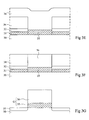
- Figures 3A to 3G illustrate, in schematic sectional view and partial, successive stages of a process formation of an isolated gate of a MOS transistor according to a mode of the present invention.
- the method according to the invention begins with the formation, on a semiconductor substrate monocrystalline 30, with a thin layer 31.
- the layer 31 is selectively etchable with respect to the substrate underlying 30. Additional elements of selection of the nature and thickness of layer 31 will be detailed in the following.
- the layer 31 is preferably a layer of oxide of silicon formed, by thermal oxidation or by CVD deposition, on a thickness corresponding to a few atomic layers, between 0.5 and 0.7 nm.
- Layer 32 is, for example, a layer of amorphous silicon, deposited at low temperature, thick between 2 and 3 nm.
- the opening 33 has, in view from above (not shown) the desired outline give an isolated gate of a MOS transistor and a socket contact of such an electrode.
- the thickness of the layer 34 is equal to the thickness that we wish to give to the isolated grid, for example, of the order of 100 to 200 nm.
- the layer 34 is made of a material capable of being selectively deposited on layer 32 without being deposited on the material constituting layer 31 present at the bottom of the opening 33.
- the layer 34 is, for example, monocrystalline germanium or polycrystalline.
- germanium on the surface of a material such as silicon from a mixture of 1 to 20% of germane in hydrogen at relatively low temperatures. , between 350 and 650 ° C.
- the growth then takes place selectively, no deposition occurs on the surfaces coated with the oxide layer 31.
- this growth is substantially vertical.
- a germanium deposit is obtained at a growth rate of 2 nm / hour by taking a flow of GeH 4 (at 10% in H 2 ) of 500 cm 3 / min, a flow of hydrogen of 20 P / min and a temperature of 450 ° C.
- the process continues, as illustrated in FIG. 3E, by depositing on the entire structure at least one conductive layer 36, for example polycrystalline silicon, so as to completely fill the opening 33.
- at least one conductive layer 36 for example polycrystalline silicon
- a gate G consisting of a gate electrode 36 isolated from the substrate 30 underlying by an insulator 35 of dielectric permittivity high.
- LDD lightly doped drain / source
- the method according to the invention advantageously allows eliminate the critical conventional etching step of the insulation wire rack. It is therefore possible to use permittivity insulators high dielectric.
- Another advantage of the process according to the present invention lies in that, given the high value of its dielectric permittivity, the thickness control of the inter-electrode insulation is less critical.
- Another advantage of the process according to the present invention is to allow recourse to a process comprising a single step of aligning a mask. Indeed, the only mask defining the opening 33 defines the grid. Then, the grid is formed self-aligned.
- Another advantage of the present invention is to obtain these results with mechanical stresses on the very limited underlying substrate. Indeed, the constraints imposed by a material such as germanium are much less than those exerted by a material such as silicon nitride.
- germanium has the advantage of being able to be eliminated under very selective and not very aggressive conditions, even over a thickness of a few hundred nanometers.
- nucleation sites OH hydroxide termination type are, for example, present in very large numbers on the surface of an oxide of silicon while they are almost nonexistent on the surface silicon.
- the preparation of the surface of the substrate 30 at the bottom of the opening 33 will be able to adapt the preparation of the surface of the substrate 30 at the bottom of the opening 33 to the insulation at high permittivity deposited.
- the nature of the layer 31 can be changed.
- layer 31 is eliminated and a preparation is carried out specific to the insulation 35 subsequently deposited.
- the preparation can also consist in the deposit, on the substrate 30, a specific initiation layer at the start of the process, before deposition (FIG. 1A) of layer 31.
- the present invention is capable of various variations and modifications that will appear to humans art.
- the invention has been described in the context of the localized formation of an insulating region intended for constitute the inter-electrode insulator of a capacitive element.
- those skilled in the art will be able to adapt the process according to the invention to the formation of a localized region of a material insulator or conductor difficult to engrave in a die given.
- the present invention has been described in case of the formation of isolated gates of MOS transistor and MIM type capacitors.
- the inter-electrode dielectric is a high permittivity dielectric, such as double grids isolated from transistors, capacitors made directly on a semiconductor substrate or in intermediate levels an integrated circuit or type capacitors metal-insulator-metal (MIM) formed in metallization levels.
- MIM metal-insulator-metal
- substrate has been designated in the present description as much a uniformly doped silicon wafer as epitaxial and / or specifically doped areas by implantation / diffusion formed on or in a solid substrate.
Landscapes
- Insulated Gate Type Field-Effect Transistor (AREA)
Abstract
Description
Claims (9)
- Procédé de formation, dans un circuit intégré, d'une région localisée d'un matériau difficilement gravable (35), caractérisé en ce qu'il comporte les étapes suivantes :former une première couche (31) d'oxyde de silicium d'épaisseur inférieure à 1 nm sur un substrat (30) ;déposer, sur la première couche, une deuxième couche (32) gravable sélectivement par rapport à la première couche ;former dans la deuxième couche une ouverture (33) selon le motif de ladite région localisée ;faire croítre sélectivement sur la deuxième couche, autour de l'ouverture, une couche de germanium (34), le matériau de la deuxième couche étant choisi pour permettre cette croissance sélective, d'où il résulte qu'il existe dans le germanium une ouverture conforme à la susdite ouverture ;déposer le matériau difficilement gravable (35) de sorte qu'il ne se dépose pas sur le germanium ;déposer une couche conductrice (36) de façon à remplir l'ouverture dans le germanium ;procéder à un aplanissement de façon à découvrir le germanium ; etéliminer le germanium et les première et deuxième couches.
- Procédé selon la revendication 1, dans lequel le substrat (30) est en silicium.
- Procédé selon la revendication 1, dans lequel la deuxième couche (32) est en silicium amorphe.
- Procédé selon la revendication 1, dans lequel la deuxième couche (32) a une épaisseur de 2 à 3 nm.
- Procédé selon la revendication 1, dans lequel la première couche d'oxyde (31) a une épaisseur de 0,5 à 0,7 nm.
- Procédé selon la revendication 1, dans lequel le germanium (34) est déposé à partir d'un mélange de germane et d'hydrogène à une température de 350 à 650°C.
- Procédé selon la revendication 1, dans lequel le matériau difficilement gravable est un isolant de permittivité diélectrique élevée (35) choisi dans le groupe comprenant MO2, MSixOy ou MAlxOy, où x et y désignent des entiers et M un atome métallique choisi parmi le groupe comprenant l'hafnium, le zirconium, le lanthane et l'aluminium.
- Procédé selon la revendication 1, dans lequel le dépôt du matériau difficilement gravable (35) est effectué par un procédé de dépôt chimique en phase vapeur par couche atomique (ALPCVD).
- Procédé selon la revendication 1, dans lequel le dépôt du matériau difficilement gravable (35) est précédé d'une élimination de la partie découverte de la première couche d'oxyde (31) au fond de l'ouverture (33) et d'un traitement propre à privilégier la croissance du matériau difficilement gravable (35) sur le substrat (30) plutôt que sur le germanium (34).
Applications Claiming Priority (2)
| Application Number | Priority Date | Filing Date | Title |
|---|---|---|---|
| FR0216800A FR2849531A1 (fr) | 2002-12-27 | 2002-12-27 | Procede de formation d'une region localisee d'un materiau difficilement gravable |
| FR0216800 | 2002-12-27 |
Publications (2)
| Publication Number | Publication Date |
|---|---|
| EP1439574A1 true EP1439574A1 (fr) | 2004-07-21 |
| EP1439574B1 EP1439574B1 (fr) | 2005-11-02 |
Family
ID=32480249
Family Applications (1)
| Application Number | Title | Priority Date | Filing Date |
|---|---|---|---|
| EP03300274A Expired - Lifetime EP1439574B1 (fr) | 2002-12-27 | 2003-12-22 | Procédé de formation d'une région localisée d'un matériau difficilement gravable |
Country Status (4)
| Country | Link |
|---|---|
| US (1) | US6969661B2 (fr) |
| EP (1) | EP1439574B1 (fr) |
| DE (1) | DE60302134D1 (fr) |
| FR (1) | FR2849531A1 (fr) |
Families Citing this family (3)
| Publication number | Priority date | Publication date | Assignee | Title |
|---|---|---|---|---|
| US6887800B1 (en) * | 2004-06-04 | 2005-05-03 | Intel Corporation | Method for making a semiconductor device with a high-k gate dielectric and metal layers that meet at a P/N junction |
| US20150024584A1 (en) * | 2013-07-17 | 2015-01-22 | Global Foundries, Inc. | Methods for forming integrated circuits with reduced replacement metal gate height variability |
| US20220108888A1 (en) * | 2020-10-04 | 2022-04-07 | Applied Materials, Inc. | Selective Deposition of Germanium |
Citations (5)
| Publication number | Priority date | Publication date | Assignee | Title |
|---|---|---|---|---|
| US6074919A (en) * | 1999-01-20 | 2000-06-13 | Advanced Micro Devices, Inc. | Method of forming an ultrathin gate dielectric |
| EP1089344A2 (fr) * | 1999-09-29 | 2001-04-04 | Kabushiki Kaisha Toshiba | Transistor à effet de champ à grille isolée et procédé pour sa fabrication |
| US6300203B1 (en) * | 2000-10-05 | 2001-10-09 | Advanced Micro Devices, Inc. | Electrolytic deposition of dielectric precursor materials for use in in-laid gate MOS transistors |
| EP1227513A2 (fr) * | 2001-01-26 | 2002-07-31 | Chartered Semiconductor Manufacturing, Inc. | Méthode de fabrication d'un diélectrique de porte ayant une constante diélectrique variable |
| EP1246254A2 (fr) * | 2001-03-28 | 2002-10-02 | Sharp Kabushiki Kaisha | Mémoire à transistor du type MFOS et son procédé de fabrication |
Family Cites Families (7)
| Publication number | Priority date | Publication date | Assignee | Title |
|---|---|---|---|---|
| US5134090A (en) * | 1982-06-18 | 1992-07-28 | At&T Bell Laboratories | Method of fabricating patterned epitaxial silicon films utilizing molecular beam epitaxy |
| US5427630A (en) * | 1994-05-09 | 1995-06-27 | International Business Machines Corporation | Mask material for low temperature selective growth of silicon or silicon alloys |
| JP2001093888A (ja) * | 1999-09-27 | 2001-04-06 | Toshiba Corp | 半導体装置の製造方法 |
| KR100639199B1 (ko) * | 2000-06-28 | 2006-10-31 | 주식회사 하이닉스반도체 | 완전 공핍형 에스오아이 소자의 제조방법 |
| US6306741B1 (en) * | 2000-07-13 | 2001-10-23 | Chartered Semiconductor Manufacturing, Inc. | Method of patterning gate electrodes with high K gate dielectrics |
| JP2003133549A (ja) * | 2001-10-29 | 2003-05-09 | Nec Corp | Mosfet及びその製造方法 |
| US6723622B2 (en) * | 2002-02-21 | 2004-04-20 | Intel Corporation | Method of forming a germanium film on a semiconductor substrate that includes the formation of a graded silicon-germanium buffer layer prior to the formation of a germanium layer |
-
2002
- 2002-12-27 FR FR0216800A patent/FR2849531A1/fr not_active Withdrawn
-
2003
- 2003-12-22 DE DE60302134T patent/DE60302134D1/de not_active Expired - Lifetime
- 2003-12-22 EP EP03300274A patent/EP1439574B1/fr not_active Expired - Lifetime
- 2003-12-23 US US10/744,680 patent/US6969661B2/en not_active Expired - Lifetime
Patent Citations (5)
| Publication number | Priority date | Publication date | Assignee | Title |
|---|---|---|---|---|
| US6074919A (en) * | 1999-01-20 | 2000-06-13 | Advanced Micro Devices, Inc. | Method of forming an ultrathin gate dielectric |
| EP1089344A2 (fr) * | 1999-09-29 | 2001-04-04 | Kabushiki Kaisha Toshiba | Transistor à effet de champ à grille isolée et procédé pour sa fabrication |
| US6300203B1 (en) * | 2000-10-05 | 2001-10-09 | Advanced Micro Devices, Inc. | Electrolytic deposition of dielectric precursor materials for use in in-laid gate MOS transistors |
| EP1227513A2 (fr) * | 2001-01-26 | 2002-07-31 | Chartered Semiconductor Manufacturing, Inc. | Méthode de fabrication d'un diélectrique de porte ayant une constante diélectrique variable |
| EP1246254A2 (fr) * | 2001-03-28 | 2002-10-02 | Sharp Kabushiki Kaisha | Mémoire à transistor du type MFOS et son procédé de fabrication |
Also Published As
| Publication number | Publication date |
|---|---|
| EP1439574B1 (fr) | 2005-11-02 |
| US20050026457A1 (en) | 2005-02-03 |
| FR2849531A1 (fr) | 2004-07-02 |
| DE60302134D1 (de) | 2005-12-08 |
| US6969661B2 (en) | 2005-11-29 |
Similar Documents
| Publication | Publication Date | Title |
|---|---|---|
| EP3127142B1 (fr) | Procédé de fabrication d'une plaque de semi-conducteur adaptée pour la fabrication d'un substrat soi, et plaque de substrat soi ainsi obtenue | |
| FR2823009A1 (fr) | Procede de fabrication d'un transistor vertical a grille isolee a faible recouvrement de la grille sur la source et sur le drain, et circuit integre comportant un tel transistor | |
| EP0463956A1 (fr) | Procédé de réalisation d'un étage d'un circuit intégré | |
| EP0258141A1 (fr) | Circuit intégré MIS tel qu'une cellule de mémoire EPROM et son procédé de fabrication | |
| FR2823010A1 (fr) | Procede de fabrication d'un transistor vertical a grille isolee a quadruple canal de conduction, et circuit integre comportant un tel transistor | |
| EP1091417A1 (fr) | Procédé fabrication d'un dispositif semi-conducteur à grille enveloppante et dispositif obtenu | |
| FR2804247A1 (fr) | Procede de realisation d'un transistor bipolaire a emetteur et base extrinseque auto-alignes | |
| FR2546664A1 (fr) | Procede de fabrication de transistors a effet de champ | |
| FR2757312A1 (fr) | Transistor mis a grille metallique auto-alignee et son procede de fabrication | |
| FR2899017A1 (fr) | Procede de realisation d'un transistor a canal comprenant du germanium | |
| FR2624304A1 (fr) | Procede pour etablir une structure d'interconnexion electrique sur un dispositif semiconducteur au silicium | |
| FR2484140A1 (fr) | Procede de fabrication d'un dispositif composite, du type metal-oxyde-semi-conducteur, d'electrode de commande a faible resistivite superficielle, et dispositif obtenu | |
| EP1074051A1 (fr) | TRANSISTOR BIPOLAIRE VERTICAL, EN PARTICULIER A BASE A HETEROJONCTION SiGe, ET PROCEDE DE FABRICATION | |
| EP1087424B1 (fr) | Procédé de fabrication d'un transistor bipolaire vertical auto-aligné | |
| EP0635880B1 (fr) | Procédé de fabrication d'un transistor en technologie silicium sur isolant | |
| EP1428247B1 (fr) | Procede de fabrication d'un transistor a effet de champ a grilles auto-alignees horizontales | |
| EP1439574B1 (fr) | Procédé de formation d'une région localisée d'un matériau difficilement gravable | |
| EP0414618A1 (fr) | Transistor MOS en couche mince avec la zone de canal reliée à la source et son procédé de fabrication | |
| EP0949667A1 (fr) | Cellule mémoire électriquement programmable | |
| WO2004057658A2 (fr) | Transistor mis a grille auto-alignee et son procede de fabrication | |
| EP0413645B1 (fr) | Procédé de fabrication de transistor MOS mésa de type silicium sur isolant | |
| EP1241704A1 (fr) | Procédé de fabrication d'un transistor bipolaire de type double polysilicum à base à hétérojonction et transistor correspondant | |
| EP0177422B1 (fr) | Procédé de réalisation de grilles en siliciure ou en silicium pour circuit intégré comportant des éléments du type grille-isolant-semiconducteur | |
| EP0403368A1 (fr) | Procédé de fabrication d'un circuit integré comportant un transistor à effet de champ à double implantation | |
| EP1223614B1 (fr) | Procédé de fabrication d'un substrat monocristallin, et circuit intégré comportant un tel substrat |
Legal Events
| Date | Code | Title | Description |
|---|---|---|---|
| PUAI | Public reference made under article 153(3) epc to a published international application that has entered the european phase |
Free format text: ORIGINAL CODE: 0009012 |
|
| AK | Designated contracting states |
Kind code of ref document: A1 Designated state(s): AT BE BG CH CY CZ DE DK EE ES FI FR GB GR HU IE IT LI LU MC NL PT RO SE SI SK TR |
|
| AX | Request for extension of the european patent |
Extension state: AL LT LV MK |
|
| 17P | Request for examination filed |
Effective date: 20050119 |
|
| AKX | Designation fees paid |
Designated state(s): DE FR GB IT |
|
| GRAP | Despatch of communication of intention to grant a patent |
Free format text: ORIGINAL CODE: EPIDOSNIGR1 |
|
| GRAP | Despatch of communication of intention to grant a patent |
Free format text: ORIGINAL CODE: EPIDOSNIGR1 |
|
| GRAS | Grant fee paid |
Free format text: ORIGINAL CODE: EPIDOSNIGR3 |
|
| GRAA | (expected) grant |
Free format text: ORIGINAL CODE: 0009210 |
|
| AK | Designated contracting states |
Kind code of ref document: B1 Designated state(s): DE FR GB IT |
|
| PG25 | Lapsed in a contracting state [announced via postgrant information from national office to epo] |
Ref country code: IT Free format text: LAPSE BECAUSE OF FAILURE TO SUBMIT A TRANSLATION OF THE DESCRIPTION OR TO PAY THE FEE WITHIN THE PRESCRIBED TIME-LIMIT;WARNING: LAPSES OF ITALIAN PATENTS WITH EFFECTIVE DATE BEFORE 2007 MAY HAVE OCCURRED AT ANY TIME BEFORE 2007. THE CORRECT EFFECTIVE DATE MAY BE DIFFERENT FROM THE ONE RECORDED. Effective date: 20051102 |
|
| REG | Reference to a national code |
Ref country code: GB Ref legal event code: FG4D Free format text: NOT ENGLISH |
|
| REF | Corresponds to: |
Ref document number: 60302134 Country of ref document: DE Date of ref document: 20051208 Kind code of ref document: P |
|
| PG25 | Lapsed in a contracting state [announced via postgrant information from national office to epo] |
Ref country code: DE Free format text: LAPSE BECAUSE OF FAILURE TO SUBMIT A TRANSLATION OF THE DESCRIPTION OR TO PAY THE FEE WITHIN THE PRESCRIBED TIME-LIMIT Effective date: 20060203 |
|
| GBT | Gb: translation of ep patent filed (gb section 77(6)(a)/1977) |
Effective date: 20060131 |
|
| PLBE | No opposition filed within time limit |
Free format text: ORIGINAL CODE: 0009261 |
|
| STAA | Information on the status of an ep patent application or granted ep patent |
Free format text: STATUS: NO OPPOSITION FILED WITHIN TIME LIMIT |
|
| 26N | No opposition filed |
Effective date: 20060803 |
|
| PGFP | Annual fee paid to national office [announced via postgrant information from national office to epo] |
Ref country code: GB Payment date: 20071129 Year of fee payment: 5 |
|
| PGFP | Annual fee paid to national office [announced via postgrant information from national office to epo] |
Ref country code: FR Payment date: 20071228 Year of fee payment: 5 |
|
| GBPC | Gb: european patent ceased through non-payment of renewal fee |
Effective date: 20081222 |
|
| REG | Reference to a national code |
Ref country code: FR Ref legal event code: ST Effective date: 20090831 |
|
| PG25 | Lapsed in a contracting state [announced via postgrant information from national office to epo] |
Ref country code: GB Free format text: LAPSE BECAUSE OF NON-PAYMENT OF DUE FEES Effective date: 20081222 |
|
| PG25 | Lapsed in a contracting state [announced via postgrant information from national office to epo] |
Ref country code: FR Free format text: LAPSE BECAUSE OF NON-PAYMENT OF DUE FEES Effective date: 20081231 |