EP1437766A2 - MOS transistor and its method of fabrication - Google Patents
MOS transistor and its method of fabrication Download PDFInfo
- Publication number
- EP1437766A2 EP1437766A2 EP20040250063 EP04250063A EP1437766A2 EP 1437766 A2 EP1437766 A2 EP 1437766A2 EP 20040250063 EP20040250063 EP 20040250063 EP 04250063 A EP04250063 A EP 04250063A EP 1437766 A2 EP1437766 A2 EP 1437766A2
- Authority
- EP
- European Patent Office
- Prior art keywords
- wsiny
- thin film
- gate
- mos transistor
- dielectric
- Prior art date
- Legal status (The legal status is an assumption and is not a legal conclusion. Google has not performed a legal analysis and makes no representation as to the accuracy of the status listed.)
- Withdrawn
Links
Images


Classifications
-
- H—ELECTRICITY
- H10—SEMICONDUCTOR DEVICES; ELECTRIC SOLID-STATE DEVICES NOT OTHERWISE PROVIDED FOR
- H10D—INORGANIC ELECTRIC SEMICONDUCTOR DEVICES
- H10D64/00—Electrodes of devices having potential barriers
- H10D64/01—Manufacture or treatment
- H10D64/013—Manufacture or treatment of electrodes having a conductor capacitively coupled to a semiconductor by an insulator
- H10D64/01302—Manufacture or treatment of electrodes having a conductor capacitively coupled to a semiconductor by an insulator the insulator being formed after the semiconductor body, the semiconductor being silicon
- H10D64/01332—Making the insulator
- H10D64/01336—Making the insulator on single crystalline silicon, e.g. chemical oxidation using a liquid
- H10D64/0134—Making the insulator on single crystalline silicon, e.g. chemical oxidation using a liquid with a treatment, e.g. annealing, after the formation of the insulator and before the formation of the conductor
-
- H—ELECTRICITY
- H10—SEMICONDUCTOR DEVICES; ELECTRIC SOLID-STATE DEVICES NOT OTHERWISE PROVIDED FOR
- H10D—INORGANIC ELECTRIC SEMICONDUCTOR DEVICES
- H10D64/00—Electrodes of devices having potential barriers
- H10D64/60—Electrodes characterised by their materials
- H10D64/66—Electrodes having a conductor capacitively coupled to a semiconductor by an insulator, e.g. MIS electrodes
- H10D64/68—Electrodes having a conductor capacitively coupled to a semiconductor by an insulator, e.g. MIS electrodes characterised by the insulator, e.g. by the gate insulator
- H10D64/681—Electrodes having a conductor capacitively coupled to a semiconductor by an insulator, e.g. MIS electrodes characterised by the insulator, e.g. by the gate insulator having a compositional variation, e.g. multilayered
- H10D64/685—Electrodes having a conductor capacitively coupled to a semiconductor by an insulator, e.g. MIS electrodes characterised by the insulator, e.g. by the gate insulator having a compositional variation, e.g. multilayered being perpendicular to the channel plane
-
- H—ELECTRICITY
- H10—SEMICONDUCTOR DEVICES; ELECTRIC SOLID-STATE DEVICES NOT OTHERWISE PROVIDED FOR
- H10D—INORGANIC ELECTRIC SEMICONDUCTOR DEVICES
- H10D64/00—Electrodes of devices having potential barriers
- H10D64/60—Electrodes characterised by their materials
- H10D64/66—Electrodes having a conductor capacitively coupled to a semiconductor by an insulator, e.g. MIS electrodes
- H10D64/68—Electrodes having a conductor capacitively coupled to a semiconductor by an insulator, e.g. MIS electrodes characterised by the insulator, e.g. by the gate insulator
- H10D64/693—Electrodes having a conductor capacitively coupled to a semiconductor by an insulator, e.g. MIS electrodes characterised by the insulator, e.g. by the gate insulator the insulator comprising nitrogen, e.g. nitrides, oxynitrides or nitrogen-doped materials
-
- H—ELECTRICITY
- H10—SEMICONDUCTOR DEVICES; ELECTRIC SOLID-STATE DEVICES NOT OTHERWISE PROVIDED FOR
- H10D—INORGANIC ELECTRIC SEMICONDUCTOR DEVICES
- H10D64/00—Electrodes of devices having potential barriers
- H10D64/01—Manufacture or treatment
- H10D64/013—Manufacture or treatment of electrodes having a conductor capacitively coupled to a semiconductor by an insulator
- H10D64/01302—Manufacture or treatment of electrodes having a conductor capacitively coupled to a semiconductor by an insulator the insulator being formed after the semiconductor body, the semiconductor being silicon
- H10D64/01332—Making the insulator
- H10D64/01336—Making the insulator on single crystalline silicon, e.g. chemical oxidation using a liquid
- H10D64/01344—Making the insulator on single crystalline silicon, e.g. chemical oxidation using a liquid in a nitrogen-containing ambient, e.g. N2O oxidation
Definitions
- the invention is in the semiconductor field and concerns MOS transistors. It particularly relates to MOS transistors with a high k gate dielectric.
- SiO2 is a stable gate dielectric material upon which the gate, typically polysilicon, may be formed.
- scaling of SiO2 gate dielectrics into the ultra-thin regime, i.e., less than ⁇ 20 ⁇ in thickness has proven ineffective because devices begin to exhibit significant leakage current, i.e., parasitic electron flow, from the channel to the gate.
- Very thin SiO2 layers are recognized to be unstable and have reached practical limits. Thicker films can be maintained to avoid leakage current, but this interferes with device scaling into the sub-micron range.
- the industry has therefore looked to high dielectric constant (k) films as substitutes for SiO2.
- a precursor for polysilicon is silane (SiH4).
- Decomposition of the precursor produces hydrogen in the ambient that can react with exposed metal oxide bonds in a conventional metal oxide dielectric.
- metal oxide dielectrics e.g., ZrO2
- Barrier layers can address this problem, but add a fabrication step. As a general principal, it is advantageous to reduce the number of fabrication steps.
- Suitable gate dielectrics that may be deposited as ultra-thin layers, e.g., about ⁇ 10nm or less, should exhibit a high dielectric constant, low interface state density and good thermal stability.
- the physical and electrical properties of high dielectric constant gate dielectrics in MOS devices aren't as well known as the properties of SiO2.
- Many high-k materials e.g., Ta2O5, HFO2, TiO2, SrTiO3, and BaSrTiO3, are thermally unstable when directly contacted with silicon and require a barrier layer.
- the barrier layers impose a thickness scaling limit.
- a preferred MOS transistor of the invention includes active regions defined in a substrate.
- An interfacial oxide thin film is upon the substrate.
- a WSiNy gate dielectric thin film is formed upon the interfacial oxide thin film and isolates a gate from the active regions.
- a preferred MOS transistor of the invention includes ultra-thin dielectric films formed of WSiNy The dielectric film properties are controlled during formation to achieve a high dielectric constant k.
- WSiNy dielectric films are formed without a barrier layer and a gate is formed directly upon the dielectric film.
- Processes of the invention include deposition processes that set deposition conditions to control the dielectric properties of the dielectric thin films.
- a particular preferred process of the invention includes controlling deposition parameters, including N2 flow, plasma power, and deposition temperature to form WSiNy dielectric films during transistor formation.
- WSiNy films normally form not as a dielectric, but as films suited for barrier layers or conductive layers.
- the invention provides a method for predictably forming dielectric WSiNy films through control of N2 flow and monitoring of plasma power during deposition.
- MOS devices In describing the invention, particular exemplary devices, formation processes, and device applications will be used for purposes of illustration. Dimensions and illustrated devices may be exaggerated for purposes of illustration and understanding of the invention. The elements of the drawings are not necessarily to scale relative to each other. Rather, emphasis has instead been placed upon clearly illustrating the invention.
- a single MOS device illustrated in conventional fashion by a two-dimensional schematic layer structure will be understood by artisans to provide teaching of three-dimensional device structures and integrations. Devices may be made and processes of the invention may be carried out with conventional integrated circuit fabrication equipment, as will also be appreciated by artisans.
- MOS transistor 8 of the invention has source and drain regions 10 defined in a substrate 12. These regions are formed conventionally, for example, by doping of a suitable semiconductor substrate.
- An exemplary substrate is a single crystal silicon wafer.
- Substrate includes a semiconductor layer having the active regions, i.e., source, drain and channel regions, and does not exclude the possibility of the substrate 12 being formed on another layer, such as a bulk layer that also might commonly be referred to as a substrate.
- the source and drain regions 10 defined in the substrate 12 are spaced apart from each other, as is conventional, defining an area of the substrate upon which a gate stack 13 may be formed.
- a channel region 14 is between the source and drain regions 10.
- the thin interfacial oxide 16 layer preferably has a thickness of less than ⁇ 1 nm.
- the gate dielectric thin film 18 is formed of dielectric WSiNy.
- the thin film 18 has a high dielectric constant k in the range of ⁇ 10 - ⁇ 35.
- the gate dielectric thin film 18 has a thickness of less than ⁇ 10nm, and preferably has a thickness in the range of ⁇ 2 - ⁇ 5 nm.
- a gate 20, for example polysilicon is formed directly upon the gate dielectric thin film 18 without use of a barrier layer. Formation of the gate 20 directly upon the gate dielectric WSiNy thin film 18 eliminates a formation process step, reducing the complexity and expense of a fabrication process to form the MOS transistor. The elimination of the barrier layer significantly simplifies transistor device and process integration.
- the WSiNy thin film 18 properties are stable during the deposition of the polysilicon gate 20, meaning any reaction with the precursors for gate deposition has a minimal or no effect on the gate dielectric thin film 18.
- Oxide spacers 22 disposed upon the source and drain regions 10 and about the gate 20 reduce hot carrier effects.
- Contacts 26 are made to the gate 20 and the source and drain regions 10. Typically, the contacts will be formed through an interlevel dielectric 27.
- the contacts 26 in preferred applications of the invention form part of a circuit interconnect pattern included in an integrated circuit connecting the MOS transistor 8 to additional devices.
- the transistor 8 operates conventionally, with source and drain voltages controlling carrier flow in the channel region 14, and the gate voltage controlling the channel.
- An initial step 30 is preparing the interface of the active region for deposition. This can include, for example, the formation of an interfacial layer. This may also include removal of excess native oxide from the interface, for example by a soft sputtering etch with Ar. In some embodiments, a thin ⁇ 1nm or less layer of native oxide is left as an interfacial layer. Embodiments of the invention may also include conventional steps prior to the preparing step 30 for forming the drain, source and channel regions of the transistor. Drain and source regions may also be formed later, for example after the gate stack, via implantation.
- ambient conditions for deposit of a thin film of dielectric WSiNy are set (step 32).
- An ambient of Ar + N2 may be used for WSiNy deposition.
- a WSi3N4 target may be sputtered in the ambient in the presence of an N2 flow to commence deposition of dielectric WSiNy (step 34).
- Reliable production of dielectric WSiNy is dependent upon the monitoring of the plasma power conditions during deposition (step 36) in a deposition chamber.
- the plasma voltage and power provide real-time information about the type of WSiNy that will deposit.
- the example graph illustrates the plasma voltage (left vertical scale graphed with diamond shaped points) and current (right vertical scale graphed with rectangle shaped points) relative to the nitrogen flow during deposition. At slightly less than about 20 sccm, plasma voltage increases rapidly while plasma current decreases rapidly. This point can vary depending on the other deposition conditions, i.e., reactor pressure, total power, relative gas flows, deposition temperature and type of target.
- the amount of nitrogen flow where plasma voltage begins to rapidly increase and plasma current begins to rapidly decrease is an accurate predictor that a dielectric WSiNy film will deposit at that and higher nitrogen flows.
- the monitoring (step 36) ensures the formation of a high-k dielectric WSiNy film.
- dielectric WSiNy films may be deposited at low temperatures, for example, room temperatures.
- the dielectric films may be annealed (step 40), for example in a rapid thermal anneal system, to relax bonds and prepare the interface and interface of the dielectric film for deposit of the gate directly thereupon.
- the annealing temperature may also be relatively low, e.g. ⁇ 450°C.
- the gate is formed (step 42) directly on the dielectric WSiNy film. Typically, this involves the formation of mask pattern with photolithography and a gate etch process, and the gate is deposited as part of a circuit interconnection pattern. After gate formation, gate oxide spacers are deposited (step 44) about the gate stack.
- doping may be conducted to form the source and drain regions of the transistor, for example, by implantation as known to those skilled in the art.
- an interlevel dielectric and source and drain contacts may then be formed to complete a transistor and its integration with other like devices.
- Transistors of the invention may be easily incorporated into integrated circuit processes without modification of conventional equipment used to form the integrated circuits. Without use of a barrier layer, a process step may be eliminated compared to processes which require a barrier layer to ensure that the gate dielectric does not degrade during deposition of the gate. This greatly simplifies transistor device and process integration
Landscapes
- Insulated Gate Type Field-Effect Transistor (AREA)
- Formation Of Insulating Films (AREA)
- Electrodes Of Semiconductors (AREA)
Abstract
The transistor has active regions (10, 14) in a substrate (12) and an interfacial oxide thin film (16) formed upon the substrate. A WSiNy gate dielectric thin film (18) formed upon the interfacial oxide thin film isolates a gate (20) from the active regions. The gate dielectric thin film has a high dielectric constant (K) in the range of 10 to 35 and a thickness in the range of 2 to 5 nanometer. An independent claim is also included for a method for forming a metal oxide semiconductor transistor gate dielectric WSiNy thin film.
Description
- The invention is in the semiconductor field and concerns MOS transistors. It particularly relates to MOS transistors with a high k gate dielectric.
- One of the industrial hurdles in the development of MOS transistors scaled down to very small sizes, for example to ~0.1 µm, is the performance of gate dielectrics. The traditional gate dielectric in silicon MOSFET devices is SiO2. SiO2 is a stable gate dielectric material upon which the gate, typically polysilicon, may be formed. However, scaling of SiO2 gate dielectrics into the ultra-thin regime, i.e., less than ~20Å in thickness, has proven ineffective because devices begin to exhibit significant leakage current, i.e., parasitic electron flow, from the channel to the gate. Very thin SiO2 layers are recognized to be unstable and have reached practical limits. Thicker films can be maintained to avoid leakage current, but this interferes with device scaling into the sub-micron range. The industry has therefore looked to high dielectric constant (k) films as substitutes for SiO2.
- The search for alternative gate dielectrics continues. One difficulty encountered in the use of alternative gate dielectrics is the need to use a separate barrier layer between a metal containing high-k dielectric and the gate, which is typically polysilicon. The function of the barrier is to prevent the reaction of precursors used to form the polysilicon with the high-k dielectric material. A precursor for polysilicon is silane (SiH4). Decomposition of the precursor produces hydrogen in the ambient that can react with exposed metal oxide bonds in a conventional metal oxide dielectric. These metal oxide dielectrics, e.g., ZrO2, provide exposed oxide bonds that react during the formation of polysilicon. This can degrade the dielectric layer and reduce its dielectric constant. Barrier layers can address this problem, but add a fabrication step. As a general principal, it is advantageous to reduce the number of fabrication steps.
- Suitable gate dielectrics that may be deposited as ultra-thin layers, e.g., about ~10nm or less, should exhibit a high dielectric constant, low interface state density and good thermal stability. The physical and electrical properties of high dielectric constant gate dielectrics in MOS devices aren't as well known as the properties of SiO2. Many high-k materials, e.g., Ta2O5, HFO2, TiO2, SrTiO3, and BaSrTiO3, are thermally unstable when directly contacted with silicon and require a barrier layer. The barrier layers impose a thickness scaling limit.
- A preferred MOS transistor of the invention includes active regions defined in a substrate. An interfacial oxide thin film is upon the substrate. A WSiNy gate dielectric thin film is formed upon the interfacial oxide thin film and isolates a gate from the active regions.
- FIG. 1 is a schematic diagram of a MOS transistor according to a preferred embodiment of the invention;
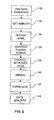
- FIG. 2 is a block diagram of a preferred embodiment method of the invention for forming a gate stack on the active region of a MOS; and
- FIG. 3 is a plot explaining exemplary growth conditions for preferred embodiment dielectric WSiNy thin films.
-
- A preferred MOS transistor of the invention includes ultra-thin dielectric films formed of WSiNy The dielectric film properties are controlled during formation to achieve a high dielectric constant k. In preferred embodiment transistors, WSiNy dielectric films are formed without a barrier layer and a gate is formed directly upon the dielectric film. Processes of the invention include deposition processes that set deposition conditions to control the dielectric properties of the dielectric thin films. A particular preferred process of the invention includes controlling deposition parameters, including N2 flow, plasma power, and deposition temperature to form WSiNy dielectric films during transistor formation. WSiNy films normally form not as a dielectric, but as films suited for barrier layers or conductive layers. The invention provides a method for predictably forming dielectric WSiNy films through control of N2 flow and monitoring of plasma power during deposition.
- The invention will now be illustrated with respect to preferred embodiment MOS devices. In describing the invention, particular exemplary devices, formation processes, and device applications will be used for purposes of illustration. Dimensions and illustrated devices may be exaggerated for purposes of illustration and understanding of the invention. The elements of the drawings are not necessarily to scale relative to each other. Rather, emphasis has instead been placed upon clearly illustrating the invention. A single MOS device illustrated in conventional fashion by a two-dimensional schematic layer structure will be understood by artisans to provide teaching of three-dimensional device structures and integrations. Devices may be made and processes of the invention may be carried out with conventional integrated circuit fabrication equipment, as will also be appreciated by artisans.
- Referring now to FIG. 1, a preferred
embodiment MOS transistor 8 of the invention is illustrated. The transistor has source anddrain regions 10 defined in asubstrate 12. These regions are formed conventionally, for example, by doping of a suitable semiconductor substrate. An exemplary substrate is a single crystal silicon wafer. Substrate, as used herein, includes a semiconductor layer having the active regions, i.e., source, drain and channel regions, and does not exclude the possibility of thesubstrate 12 being formed on another layer, such as a bulk layer that also might commonly be referred to as a substrate. The source anddrain regions 10 defined in thesubstrate 12 are spaced apart from each other, as is conventional, defining an area of the substrate upon which a gate stack 13 may be formed. Achannel region 14 is between the source anddrain regions 10. An interfacial oxidethin film 16, e.g., a native oxide or SiO2, upon thesubstrate 12 facilitates the bond of a thindielectric film 18. The thininterfacial oxide 16 layer preferably has a thickness of less than ~1 nm. In accordance with the invention, the gate dielectricthin film 18 is formed of dielectric WSiNy. Thethin film 18 has a high dielectric constant k in the range of ~10 - ~35. The gate dielectricthin film 18 has a thickness of less than ~10nm, and preferably has a thickness in the range of ~2 - ~5 nm. - According to the preferred embodiment of FIG. 1, a
gate 20, for example polysilicon, is formed directly upon the gate dielectricthin film 18 without use of a barrier layer. Formation of thegate 20 directly upon the gate dielectric WSiNythin film 18 eliminates a formation process step, reducing the complexity and expense of a fabrication process to form the MOS transistor. The elimination of the barrier layer significantly simplifies transistor device and process integration. The WSiNythin film 18 properties are stable during the deposition of thepolysilicon gate 20, meaning any reaction with the precursors for gate deposition has a minimal or no effect on the gate dielectricthin film 18. -
Oxide spacers 22 disposed upon the source anddrain regions 10 and about thegate 20 reduce hot carrier effects.Contacts 26 are made to thegate 20 and the source anddrain regions 10. Typically, the contacts will be formed through an interlevel dielectric 27. Thecontacts 26 in preferred applications of the invention form part of a circuit interconnect pattern included in an integrated circuit connecting theMOS transistor 8 to additional devices. Thetransistor 8 operates conventionally, with source and drain voltages controlling carrier flow in thechannel region 14, and the gate voltage controlling the channel. - A preferred method for forming a gate stack on the active region of a MOS transistor will now be discussed with respect to FIG. 2. An
initial step 30 is preparing the interface of the active region for deposition. This can include, for example, the formation of an interfacial layer. This may also include removal of excess native oxide from the interface, for example by a soft sputtering etch with Ar. In some embodiments, a thin ~1nm or less layer of native oxide is left as an interfacial layer. Embodiments of the invention may also include conventional steps prior to the preparingstep 30 for forming the drain, source and channel regions of the transistor. Drain and source regions may also be formed later, for example after the gate stack, via implantation. After preparing the active region interface, ambient conditions for deposit of a thin film of dielectric WSiNy are set (step 32). An ambient of Ar + N2 may be used for WSiNy deposition. A WSi3N4 target may be sputtered in the ambient in the presence of an N2 flow to commence deposition of dielectric WSiNy (step 34). - Reliable production of dielectric WSiNy is dependent upon the monitoring of the plasma power conditions during deposition (step 36) in a deposition chamber. Referring now to FIG. 3, the plasma voltage and power provide real-time information about the type of WSiNy that will deposit. The example graph illustrates the plasma voltage (left vertical scale graphed with diamond shaped points) and current (right vertical scale graphed with rectangle shaped points) relative to the nitrogen flow during deposition. At slightly less than about 20 sccm, plasma voltage increases rapidly while plasma current decreases rapidly. This point can vary depending on the other deposition conditions, i.e., reactor pressure, total power, relative gas flows, deposition temperature and type of target. In any case, the amount of nitrogen flow where plasma voltage begins to rapidly increase and plasma current begins to rapidly decrease is an accurate predictor that a dielectric WSiNy film will deposit at that and higher nitrogen flows. In conjunction with the control of nitrogen flow (step 38), the monitoring (step 36) ensures the formation of a high-k dielectric WSiNy film.
- Advantageously, dielectric WSiNy films may be deposited at low temperatures, for example, room temperatures. The dielectric films may be annealed (step 40), for example in a rapid thermal anneal system, to relax bonds and prepare the interface and interface of the dielectric film for deposit of the gate directly thereupon. The annealing temperature may also be relatively low, e.g. ~450°C. Subsequently, the gate is formed (step 42) directly on the dielectric WSiNy film. Typically, this involves the formation of mask pattern with photolithography and a gate etch process, and the gate is deposited as part of a circuit interconnection pattern. After gate formation, gate oxide spacers are deposited (step 44) about the gate stack. After the spacers, doping may be conducted to form the source and drain regions of the transistor, for example, by implantation as known to those skilled in the art. In an integrated circuit formation process an interlevel dielectric and source and drain contacts may then be formed to complete a transistor and its integration with other like devices.
- Transistors of the invention may be easily incorporated into integrated circuit processes without modification of conventional equipment used to form the integrated circuits. Without use of a barrier layer, a process step may be eliminated compared to processes which require a barrier layer to ensure that the gate dielectric does not degrade during deposition of the gate. This greatly simplifies transistor device and process integration
- While a specific embodiment of the present invention has been shown and described, it should be understood that other modifications, substitutions and alternatives are apparent to one of ordinary skill in the art. Such modifications, substitutions and alternatives can be made without departing from the scope of the invention, which should be determined from the appended claims.
- Various features of the invention are set forth in the appended claims.
Claims (10)
- A MOS transistor, comprising:thin film.a substrate (12);active regions (10,14) in said substrate;an interfacial oxide thin film (16) upon said substrate;a WSiNy gate dielectric thin film (18) formed upon said interfacial oxide thin film; anda gate (20) isolated from said active regions by said WSiNy gate dielectric
- The MOS transistor of claim 1, wherein said WSiNy gate dielectric thin film has a thickness of less than ~10nm.
- The MOS transistor of claim 2, wherein said WSiNy gate dielectric thin film has a thickness in the range of ~2 ― ~5nm.
- The MOS transistor of claim 1, further comprising spacers (22) disposed about said gate to reduce hot carrier effects.
- The MOS transistor of claim 4, wherein said active regions comprise source, drain (10) and channel (14) regions, the transistor further comprising device contacts (26) to said gate and said source and drain regions.
- The MOS transistor of claim 5, wherein said device contacts comprise part of a circuit interconnect pattern.
- The MOS transistor of claim 6, formed as part of an integrated circuit.
- A method for forming a MOS transistor gate dielectric WSiNy thin film, the method comprising steps of:preparing an interface for deposit of the gate dielectric WSiNy thin film;setting ambient conditions for deposit of the gate dielectric WSiNy thin film; anddepositing the gate dielectric WSiNy thin film.
- The method according to claim 8, wherein said step of setting comprises controlling nitrogen flow to deposit dielectric WSiNy.
- The method according to claim 9, wherein said step of depositing comprises monitoring plasma power during deposition and controlling the nitrogen flow to deposit dielectric WSiNy.
Applications Claiming Priority (2)
| Application Number | Priority Date | Filing Date | Title |
|---|---|---|---|
| US341646 | 1989-04-21 | ||
| US10/341,646 US20040135218A1 (en) | 2003-01-13 | 2003-01-13 | MOS transistor with high k gate dielectric |
Publications (1)
| Publication Number | Publication Date |
|---|---|
| EP1437766A2 true EP1437766A2 (en) | 2004-07-14 |
Family
ID=32507500
Family Applications (1)
| Application Number | Title | Priority Date | Filing Date |
|---|---|---|---|
| EP20040250063 Withdrawn EP1437766A2 (en) | 2003-01-13 | 2004-01-08 | MOS transistor and its method of fabrication |
Country Status (4)
| Country | Link |
|---|---|
| US (1) | US20040135218A1 (en) |
| EP (1) | EP1437766A2 (en) |
| JP (1) | JP2004221580A (en) |
| TW (1) | TW200412671A (en) |
Families Citing this family (1)
| Publication number | Priority date | Publication date | Assignee | Title |
|---|---|---|---|---|
| RU2723982C1 (en) * | 2019-08-06 | 2020-06-18 | Федеральное государственное бюджетное образовательное учреждение высшего образования "Кабардино-Балкарский государственный университет им. Х.М. Бербекова" (КБГУ) | Semiconductor device manufacturing method |
Family Cites Families (28)
| Publication number | Priority date | Publication date | Assignee | Title |
|---|---|---|---|---|
| US81862A (en) * | 1868-09-08 | Alfred arnemann | ||
| US46789A (en) * | 1865-03-14 | Peeey g | ||
| US5440174A (en) * | 1992-10-20 | 1995-08-08 | Matsushita Electric Industrial Co., Ltd. | Plurality of passive elements in a semiconductor integrated circuit and semiconductor integrated circuit in which passive elements are arranged |
| JPH08125412A (en) * | 1994-10-19 | 1996-05-17 | Mitsubishi Electric Corp | Transmission line and manufacturing method thereof |
| US5907188A (en) * | 1995-08-25 | 1999-05-25 | Kabushiki Kaisha Toshiba | Semiconductor device with conductive oxidation preventing film and method for manufacturing the same |
| US5916634A (en) * | 1996-10-01 | 1999-06-29 | Sandia Corporation | Chemical vapor deposition of W-Si-N and W-B-N |
| JPH10223900A (en) * | 1996-12-03 | 1998-08-21 | Toshiba Corp | Semiconductor device and method of manufacturing semiconductor device |
| US5872376A (en) * | 1997-03-06 | 1999-02-16 | Advanced Micro Devices, Inc. | Oxide formation technique using thin film silicon deposition |
| US6084279A (en) * | 1997-03-31 | 2000-07-04 | Motorola Inc. | Semiconductor device having a metal containing layer overlying a gate dielectric |
| JPH11233451A (en) * | 1997-10-07 | 1999-08-27 | Texas Instr Inc <Ti> | CVD-based process for producing stable, low-resistance poly-metal gate electrodes |
| US6861356B2 (en) * | 1997-11-05 | 2005-03-01 | Tokyo Electron Limited | Method of forming a barrier film and method of forming wiring structure and electrodes of semiconductor device having a barrier film |
| US6103607A (en) * | 1998-09-15 | 2000-08-15 | Lucent Technologies | Manufacture of MOSFET devices |
| US6339246B1 (en) * | 1998-12-11 | 2002-01-15 | Isik C. Kizilyalli | Tungsten silicide nitride as an electrode for tantalum pentoxide devices |
| KR100296126B1 (en) * | 1998-12-22 | 2001-08-07 | 박종섭 | Gate electrode formation method of highly integrated memory device |
| US6294807B1 (en) * | 1999-02-26 | 2001-09-25 | Agere Systems Guardian Corp. | Semiconductor device structure including a tantalum pentoxide layer sandwiched between silicon nitride layers |
| US6444478B1 (en) * | 1999-08-31 | 2002-09-03 | Micron Technology, Inc. | Dielectric films and methods of forming same |
| US6383879B1 (en) * | 1999-12-03 | 2002-05-07 | Agere Systems Guardian Corp. | Semiconductor device having a metal gate with a work function compatible with a semiconductor device |
| JP2001185506A (en) * | 1999-12-22 | 2001-07-06 | Mitsubishi Electric Corp | Method for manufacturing semiconductor device |
| US6184072B1 (en) * | 2000-05-17 | 2001-02-06 | Motorola, Inc. | Process for forming a high-K gate dielectric |
| US6383873B1 (en) * | 2000-05-18 | 2002-05-07 | Motorola, Inc. | Process for forming a structure |
| WO2002004704A2 (en) * | 2000-07-11 | 2002-01-17 | Applied Materials, Inc. | Method and apparatus for patching electrochemically deposited layers using electroless deposited materials |
| US20020089023A1 (en) * | 2001-01-05 | 2002-07-11 | Motorola, Inc. | Low leakage current metal oxide-nitrides and method of fabricating same |
| US6541280B2 (en) * | 2001-03-20 | 2003-04-01 | Motorola, Inc. | High K dielectric film |
| US6518106B2 (en) * | 2001-05-26 | 2003-02-11 | Motorola, Inc. | Semiconductor device and a method therefor |
| US7037862B2 (en) * | 2001-06-13 | 2006-05-02 | Micron Technology, Inc. | Dielectric layer forming method and devices formed therewith |
| JP3781666B2 (en) * | 2001-11-29 | 2006-05-31 | エルピーダメモリ株式会社 | Method for forming gate electrode and gate electrode structure |
| US6696332B2 (en) * | 2001-12-26 | 2004-02-24 | Texas Instruments Incorporated | Bilayer deposition to avoid unwanted interfacial reactions during high K gate dielectric processing |
| US6794281B2 (en) * | 2002-05-20 | 2004-09-21 | Freescale Semiconductor, Inc. | Dual metal gate transistors for CMOS process |
-
2003
- 2003-01-13 US US10/341,646 patent/US20040135218A1/en not_active Abandoned
- 2003-07-28 TW TW092120522A patent/TW200412671A/en unknown
-
2004
- 2004-01-08 JP JP2004002826A patent/JP2004221580A/en active Pending
- 2004-01-08 EP EP20040250063 patent/EP1437766A2/en not_active Withdrawn
Also Published As
| Publication number | Publication date |
|---|---|
| US20040135218A1 (en) | 2004-07-15 |
| JP2004221580A (en) | 2004-08-05 |
| TW200412671A (en) | 2004-07-16 |
Similar Documents
| Publication | Publication Date | Title |
|---|---|---|
| US6060755A (en) | Aluminum-doped zirconium dielectric film transistor structure and deposition method for same | |
| US6620713B2 (en) | Interfacial layer for gate electrode and high-k dielectric layer and methods of fabrication | |
| US7541650B2 (en) | Gate electrode structures | |
| KR101065045B1 (en) | How to form metal gate structure by adjusting work function by silicon incorporation | |
| JP4165076B2 (en) | Semiconductor device having high dielectric constant insulating film | |
| US8088678B2 (en) | Semiconductor manufacturing apparatus and method | |
| KR20020005432A (en) | Doped zirconia, or zirconia-like, dielectric film transistor structure and deposition method for same | |
| US20040070036A1 (en) | ULSI MOS with high dielectric constant gate insulator | |
| US7863083B2 (en) | High temperature processing compatible metal gate electrode for pFETS and methods for fabrication | |
| US6100188A (en) | Stable and low resistance metal/barrier/silicon stack structure and related process for manufacturing | |
| KR20230140576A (en) | MOSFET gate engineering using dipole films | |
| TWI393176B (en) | Method for manufacturing a metal oxide germanium device having a non-cerium oxide gate dielectric | |
| US6066519A (en) | Semiconductor device having an outgassed oxide layer and fabrication thereof | |
| KR100671722B1 (en) | Silicon Gate Field Effect Transistor Device Manufacturing Method | |
| EP1437766A2 (en) | MOS transistor and its method of fabrication | |
| US6624093B1 (en) | Method of producing high dielectric insulator for integrated circuit | |
| JP2004179612A (en) | Method for manufacturing semiconductor device | |
| KR100379621B1 (en) | Gate insulator of MOS transistor and method for fabricating the same | |
| TW202226596A (en) | Pmos high-k metal gates | |
| CN114373678B (en) | A method for enhancing multi-layer thin film silicide by ion implantation | |
| US20080242114A1 (en) | Thermal anneal method for a high-k dielectric | |
| KR100680970B1 (en) | Gate Forming Method of Semiconductor Device | |
| KR100364524B1 (en) | Method for Forming MOS Transistor Having Single-Layer Gate Structure Made of Tungsten Silicide | |
| Gopalan | by Sundararaman Gopalan | |
| Nieh | An evaluation of the electrical, material, and reliability characteristics and process viability of ZrO₂ and ZrOxNy for future generation MOS gate dielectric |
Legal Events
| Date | Code | Title | Description |
|---|---|---|---|
| PUAI | Public reference made under article 153(3) epc to a published international application that has entered the european phase |
Free format text: ORIGINAL CODE: 0009012 |
|
| AK | Designated contracting states |
Kind code of ref document: A2 Designated state(s): AT BE BG CH CY CZ DE DK EE ES FI FR GB GR HU IE IT LI LU MC NL PT RO SE SI SK TR |
|
| AX | Request for extension of the european patent |
Extension state: AL LT LV MK |
|
| STAA | Information on the status of an ep patent application or granted ep patent |
Free format text: STATUS: THE APPLICATION HAS BEEN WITHDRAWN |
|
| 18W | Application withdrawn |
Effective date: 20041124 |