EP1436865B1 - MICROCHIPLASER FÜR DEN MITTLEREN IR-BEREICH: ZnS:Cr-2+-LASER MIT SÄTTIGBAREM ABSORBIERERMATERIAL - Google Patents
MICROCHIPLASER FÜR DEN MITTLEREN IR-BEREICH: ZnS:Cr-2+-LASER MIT SÄTTIGBAREM ABSORBIERERMATERIAL Download PDFInfo
- Publication number
- EP1436865B1 EP1436865B1 EP02761727.3A EP02761727A EP1436865B1 EP 1436865 B1 EP1436865 B1 EP 1436865B1 EP 02761727 A EP02761727 A EP 02761727A EP 1436865 B1 EP1436865 B1 EP 1436865B1
- Authority
- EP
- European Patent Office
- Prior art keywords
- crystal
- laser
- zns
- microchip
- transition metal
- Prior art date
- Legal status (The legal status is an assumption and is not a legal conclusion. Google has not performed a legal analysis and makes no representation as to the accuracy of the status listed.)
- Expired - Lifetime
Links
Images







Classifications
-
- H—ELECTRICITY
- H01—ELECTRIC ELEMENTS
- H01S—DEVICES USING THE PROCESS OF LIGHT AMPLIFICATION BY STIMULATED EMISSION OF RADIATION [LASER] TO AMPLIFY OR GENERATE LIGHT; DEVICES USING STIMULATED EMISSION OF ELECTROMAGNETIC RADIATION IN WAVE RANGES OTHER THAN OPTICAL
- H01S3/00—Lasers, i.e. devices using stimulated emission of electromagnetic radiation in the infrared, visible or ultraviolet wave range
- H01S3/05—Construction or shape of optical resonators; Accommodation of active medium therein; Shape of active medium
- H01S3/08—Construction or shape of optical resonators or components thereof
- H01S3/08018—Mode suppression
- H01S3/0804—Transverse or lateral modes
- H01S3/0805—Transverse or lateral modes by apertures, e.g. pin-holes or knife-edges
-
- C—CHEMISTRY; METALLURGY
- C30—CRYSTAL GROWTH
- C30B—SINGLE-CRYSTAL GROWTH; UNIDIRECTIONAL SOLIDIFICATION OF EUTECTIC MATERIAL OR UNIDIRECTIONAL DEMIXING OF EUTECTOID MATERIAL; REFINING BY ZONE-MELTING OF MATERIAL; PRODUCTION OF A HOMOGENEOUS POLYCRYSTALLINE MATERIAL WITH DEFINED STRUCTURE; SINGLE CRYSTALS OR HOMOGENEOUS POLYCRYSTALLINE MATERIAL WITH DEFINED STRUCTURE; AFTER-TREATMENT OF SINGLE CRYSTALS OR A HOMOGENEOUS POLYCRYSTALLINE MATERIAL WITH DEFINED STRUCTURE; APPARATUS THEREFOR
- C30B31/00—Diffusion or doping processes for single crystals or homogeneous polycrystalline material with defined structure; Apparatus therefor
-
- C—CHEMISTRY; METALLURGY
- C30—CRYSTAL GROWTH
- C30B—SINGLE-CRYSTAL GROWTH; UNIDIRECTIONAL SOLIDIFICATION OF EUTECTIC MATERIAL OR UNIDIRECTIONAL DEMIXING OF EUTECTOID MATERIAL; REFINING BY ZONE-MELTING OF MATERIAL; PRODUCTION OF A HOMOGENEOUS POLYCRYSTALLINE MATERIAL WITH DEFINED STRUCTURE; SINGLE CRYSTALS OR HOMOGENEOUS POLYCRYSTALLINE MATERIAL WITH DEFINED STRUCTURE; AFTER-TREATMENT OF SINGLE CRYSTALS OR A HOMOGENEOUS POLYCRYSTALLINE MATERIAL WITH DEFINED STRUCTURE; APPARATUS THEREFOR
- C30B29/00—Single crystals or homogeneous polycrystalline material with defined structure characterised by the material or by their shape
- C30B29/10—Inorganic compounds or compositions
- C30B29/46—Sulfur-, selenium- or tellurium-containing compounds
- C30B29/48—AIIBVI compounds wherein A is Zn, Cd or Hg, and B is S, Se or Te
-
- C—CHEMISTRY; METALLURGY
- C30—CRYSTAL GROWTH
- C30B—SINGLE-CRYSTAL GROWTH; UNIDIRECTIONAL SOLIDIFICATION OF EUTECTIC MATERIAL OR UNIDIRECTIONAL DEMIXING OF EUTECTOID MATERIAL; REFINING BY ZONE-MELTING OF MATERIAL; PRODUCTION OF A HOMOGENEOUS POLYCRYSTALLINE MATERIAL WITH DEFINED STRUCTURE; SINGLE CRYSTALS OR HOMOGENEOUS POLYCRYSTALLINE MATERIAL WITH DEFINED STRUCTURE; AFTER-TREATMENT OF SINGLE CRYSTALS OR A HOMOGENEOUS POLYCRYSTALLINE MATERIAL WITH DEFINED STRUCTURE; APPARATUS THEREFOR
- C30B31/00—Diffusion or doping processes for single crystals or homogeneous polycrystalline material with defined structure; Apparatus therefor
- C30B31/02—Diffusion or doping processes for single crystals or homogeneous polycrystalline material with defined structure; Apparatus therefor by contacting with diffusion materials in the solid state
-
- H—ELECTRICITY
- H01—ELECTRIC ELEMENTS
- H01S—DEVICES USING THE PROCESS OF LIGHT AMPLIFICATION BY STIMULATED EMISSION OF RADIATION [LASER] TO AMPLIFY OR GENERATE LIGHT; DEVICES USING STIMULATED EMISSION OF ELECTROMAGNETIC RADIATION IN WAVE RANGES OTHER THAN OPTICAL
- H01S3/00—Lasers, i.e. devices using stimulated emission of electromagnetic radiation in the infrared, visible or ultraviolet wave range
- H01S3/05—Construction or shape of optical resonators; Accommodation of active medium therein; Shape of active medium
- H01S3/06—Construction or shape of active medium
- H01S3/0602—Crystal lasers or glass lasers
- H01S3/0604—Crystal lasers or glass lasers in the form of a plate or disc
-
- H—ELECTRICITY
- H01—ELECTRIC ELEMENTS
- H01S—DEVICES USING THE PROCESS OF LIGHT AMPLIFICATION BY STIMULATED EMISSION OF RADIATION [LASER] TO AMPLIFY OR GENERATE LIGHT; DEVICES USING STIMULATED EMISSION OF ELECTROMAGNETIC RADIATION IN WAVE RANGES OTHER THAN OPTICAL
- H01S3/00—Lasers, i.e. devices using stimulated emission of electromagnetic radiation in the infrared, visible or ultraviolet wave range
- H01S3/05—Construction or shape of optical resonators; Accommodation of active medium therein; Shape of active medium
- H01S3/06—Construction or shape of active medium
- H01S3/0627—Construction or shape of active medium the resonator being monolithic, e.g. microlaser
-
- H—ELECTRICITY
- H01—ELECTRIC ELEMENTS
- H01S—DEVICES USING THE PROCESS OF LIGHT AMPLIFICATION BY STIMULATED EMISSION OF RADIATION [LASER] TO AMPLIFY OR GENERATE LIGHT; DEVICES USING STIMULATED EMISSION OF ELECTROMAGNETIC RADIATION IN WAVE RANGES OTHER THAN OPTICAL
- H01S3/00—Lasers, i.e. devices using stimulated emission of electromagnetic radiation in the infrared, visible or ultraviolet wave range
- H01S3/05—Construction or shape of optical resonators; Accommodation of active medium therein; Shape of active medium
- H01S3/08—Construction or shape of optical resonators or components thereof
- H01S3/08004—Construction or shape of optical resonators or components thereof incorporating a dispersive element, e.g. a prism for wavelength selection
- H01S3/08009—Construction or shape of optical resonators or components thereof incorporating a dispersive element, e.g. a prism for wavelength selection using a diffraction grating
-
- H—ELECTRICITY
- H01—ELECTRIC ELEMENTS
- H01S—DEVICES USING THE PROCESS OF LIGHT AMPLIFICATION BY STIMULATED EMISSION OF RADIATION [LASER] TO AMPLIFY OR GENERATE LIGHT; DEVICES USING STIMULATED EMISSION OF ELECTROMAGNETIC RADIATION IN WAVE RANGES OTHER THAN OPTICAL
- H01S3/00—Lasers, i.e. devices using stimulated emission of electromagnetic radiation in the infrared, visible or ultraviolet wave range
- H01S3/05—Construction or shape of optical resonators; Accommodation of active medium therein; Shape of active medium
- H01S3/08—Construction or shape of optical resonators or components thereof
- H01S3/08086—Multiple-wavelength emission
-
- H—ELECTRICITY
- H01—ELECTRIC ELEMENTS
- H01S—DEVICES USING THE PROCESS OF LIGHT AMPLIFICATION BY STIMULATED EMISSION OF RADIATION [LASER] TO AMPLIFY OR GENERATE LIGHT; DEVICES USING STIMULATED EMISSION OF ELECTROMAGNETIC RADIATION IN WAVE RANGES OTHER THAN OPTICAL
- H01S3/00—Lasers, i.e. devices using stimulated emission of electromagnetic radiation in the infrared, visible or ultraviolet wave range
- H01S3/09—Processes or apparatus for excitation, e.g. pumping
- H01S3/091—Processes or apparatus for excitation, e.g. pumping using optical pumping
- H01S3/094—Processes or apparatus for excitation, e.g. pumping using optical pumping by coherent light
- H01S3/094042—Processes or apparatus for excitation, e.g. pumping using optical pumping by coherent light of a fibre laser
-
- H—ELECTRICITY
- H01—ELECTRIC ELEMENTS
- H01S—DEVICES USING THE PROCESS OF LIGHT AMPLIFICATION BY STIMULATED EMISSION OF RADIATION [LASER] TO AMPLIFY OR GENERATE LIGHT; DEVICES USING STIMULATED EMISSION OF ELECTROMAGNETIC RADIATION IN WAVE RANGES OTHER THAN OPTICAL
- H01S3/00—Lasers, i.e. devices using stimulated emission of electromagnetic radiation in the infrared, visible or ultraviolet wave range
- H01S3/09—Processes or apparatus for excitation, e.g. pumping
- H01S3/091—Processes or apparatus for excitation, e.g. pumping using optical pumping
- H01S3/094—Processes or apparatus for excitation, e.g. pumping using optical pumping by coherent light
- H01S3/094042—Processes or apparatus for excitation, e.g. pumping using optical pumping by coherent light of a fibre laser
- H01S3/094046—Processes or apparatus for excitation, e.g. pumping using optical pumping by coherent light of a fibre laser of a Raman fibre laser
-
- H—ELECTRICITY
- H01—ELECTRIC ELEMENTS
- H01S—DEVICES USING THE PROCESS OF LIGHT AMPLIFICATION BY STIMULATED EMISSION OF RADIATION [LASER] TO AMPLIFY OR GENERATE LIGHT; DEVICES USING STIMULATED EMISSION OF ELECTROMAGNETIC RADIATION IN WAVE RANGES OTHER THAN OPTICAL
- H01S3/00—Lasers, i.e. devices using stimulated emission of electromagnetic radiation in the infrared, visible or ultraviolet wave range
- H01S3/09—Processes or apparatus for excitation, e.g. pumping
- H01S3/091—Processes or apparatus for excitation, e.g. pumping using optical pumping
- H01S3/094—Processes or apparatus for excitation, e.g. pumping using optical pumping by coherent light
- H01S3/0941—Processes or apparatus for excitation, e.g. pumping using optical pumping by coherent light of a laser diode
- H01S3/09415—Processes or apparatus for excitation, e.g. pumping using optical pumping by coherent light of a laser diode the pumping beam being parallel to the lasing mode of the pumped medium, e.g. end-pumping
-
- H—ELECTRICITY
- H01—ELECTRIC ELEMENTS
- H01S—DEVICES USING THE PROCESS OF LIGHT AMPLIFICATION BY STIMULATED EMISSION OF RADIATION [LASER] TO AMPLIFY OR GENERATE LIGHT; DEVICES USING STIMULATED EMISSION OF ELECTROMAGNETIC RADIATION IN WAVE RANGES OTHER THAN OPTICAL
- H01S3/00—Lasers, i.e. devices using stimulated emission of electromagnetic radiation in the infrared, visible or ultraviolet wave range
- H01S3/10—Controlling the intensity, frequency, phase, polarisation or direction of the emitted radiation, e.g. switching, gating, modulating or demodulating
- H01S3/105—Controlling the intensity, frequency, phase, polarisation or direction of the emitted radiation, e.g. switching, gating, modulating or demodulating by controlling the mutual position or the reflecting properties of the reflectors of the cavity, e.g. by controlling the cavity length
- H01S3/1055—Controlling the intensity, frequency, phase, polarisation or direction of the emitted radiation, e.g. switching, gating, modulating or demodulating by controlling the mutual position or the reflecting properties of the reflectors of the cavity, e.g. by controlling the cavity length one of the reflectors being constituted by a diffraction grating
-
- H—ELECTRICITY
- H01—ELECTRIC ELEMENTS
- H01S—DEVICES USING THE PROCESS OF LIGHT AMPLIFICATION BY STIMULATED EMISSION OF RADIATION [LASER] TO AMPLIFY OR GENERATE LIGHT; DEVICES USING STIMULATED EMISSION OF ELECTROMAGNETIC RADIATION IN WAVE RANGES OTHER THAN OPTICAL
- H01S3/00—Lasers, i.e. devices using stimulated emission of electromagnetic radiation in the infrared, visible or ultraviolet wave range
- H01S3/10—Controlling the intensity, frequency, phase, polarisation or direction of the emitted radiation, e.g. switching, gating, modulating or demodulating
- H01S3/106—Controlling the intensity, frequency, phase, polarisation or direction of the emitted radiation, e.g. switching, gating, modulating or demodulating by controlling devices placed within the cavity
- H01S3/108—Controlling the intensity, frequency, phase, polarisation or direction of the emitted radiation, e.g. switching, gating, modulating or demodulating by controlling devices placed within the cavity using non-linear optical devices, e.g. exhibiting Brillouin or Raman scattering
-
- H—ELECTRICITY
- H01—ELECTRIC ELEMENTS
- H01S—DEVICES USING THE PROCESS OF LIGHT AMPLIFICATION BY STIMULATED EMISSION OF RADIATION [LASER] TO AMPLIFY OR GENERATE LIGHT; DEVICES USING STIMULATED EMISSION OF ELECTROMAGNETIC RADIATION IN WAVE RANGES OTHER THAN OPTICAL
- H01S3/00—Lasers, i.e. devices using stimulated emission of electromagnetic radiation in the infrared, visible or ultraviolet wave range
- H01S3/10—Controlling the intensity, frequency, phase, polarisation or direction of the emitted radiation, e.g. switching, gating, modulating or demodulating
- H01S3/11—Mode locking; Q-switching; Other giant-pulse techniques, e.g. cavity dumping
- H01S3/1123—Q-switching
- H01S3/115—Q-switching using intracavity electro-optic devices
-
- H—ELECTRICITY
- H01—ELECTRIC ELEMENTS
- H01S—DEVICES USING THE PROCESS OF LIGHT AMPLIFICATION BY STIMULATED EMISSION OF RADIATION [LASER] TO AMPLIFY OR GENERATE LIGHT; DEVICES USING STIMULATED EMISSION OF ELECTROMAGNETIC RADIATION IN WAVE RANGES OTHER THAN OPTICAL
- H01S3/00—Lasers, i.e. devices using stimulated emission of electromagnetic radiation in the infrared, visible or ultraviolet wave range
- H01S3/10—Controlling the intensity, frequency, phase, polarisation or direction of the emitted radiation, e.g. switching, gating, modulating or demodulating
- H01S3/11—Mode locking; Q-switching; Other giant-pulse techniques, e.g. cavity dumping
- H01S3/1123—Q-switching
- H01S3/117—Q-switching using intracavity acousto-optic devices
-
- H—ELECTRICITY
- H01—ELECTRIC ELEMENTS
- H01S—DEVICES USING THE PROCESS OF LIGHT AMPLIFICATION BY STIMULATED EMISSION OF RADIATION [LASER] TO AMPLIFY OR GENERATE LIGHT; DEVICES USING STIMULATED EMISSION OF ELECTROMAGNETIC RADIATION IN WAVE RANGES OTHER THAN OPTICAL
- H01S3/00—Lasers, i.e. devices using stimulated emission of electromagnetic radiation in the infrared, visible or ultraviolet wave range
- H01S3/14—Lasers, i.e. devices using stimulated emission of electromagnetic radiation in the infrared, visible or ultraviolet wave range characterised by the material used as the active medium
- H01S3/16—Solid materials
- H01S3/1601—Solid materials characterised by an active (lasing) ion
- H01S3/162—Solid materials characterised by an active (lasing) ion transition metal
-
- H—ELECTRICITY
- H01—ELECTRIC ELEMENTS
- H01S—DEVICES USING THE PROCESS OF LIGHT AMPLIFICATION BY STIMULATED EMISSION OF RADIATION [LASER] TO AMPLIFY OR GENERATE LIGHT; DEVICES USING STIMULATED EMISSION OF ELECTROMAGNETIC RADIATION IN WAVE RANGES OTHER THAN OPTICAL
- H01S3/00—Lasers, i.e. devices using stimulated emission of electromagnetic radiation in the infrared, visible or ultraviolet wave range
- H01S3/14—Lasers, i.e. devices using stimulated emission of electromagnetic radiation in the infrared, visible or ultraviolet wave range characterised by the material used as the active medium
- H01S3/16—Solid materials
- H01S3/1601—Solid materials characterised by an active (lasing) ion
- H01S3/162—Solid materials characterised by an active (lasing) ion transition metal
- H01S3/1623—Solid materials characterised by an active (lasing) ion transition metal chromium, e.g. Alexandrite
-
- H—ELECTRICITY
- H01—ELECTRIC ELEMENTS
- H01S—DEVICES USING THE PROCESS OF LIGHT AMPLIFICATION BY STIMULATED EMISSION OF RADIATION [LASER] TO AMPLIFY OR GENERATE LIGHT; DEVICES USING STIMULATED EMISSION OF ELECTROMAGNETIC RADIATION IN WAVE RANGES OTHER THAN OPTICAL
- H01S2301/00—Functional characteristics
- H01S2301/04—Gain spectral shaping, flattening
-
- H—ELECTRICITY
- H01—ELECTRIC ELEMENTS
- H01S—DEVICES USING THE PROCESS OF LIGHT AMPLIFICATION BY STIMULATED EMISSION OF RADIATION [LASER] TO AMPLIFY OR GENERATE LIGHT; DEVICES USING STIMULATED EMISSION OF ELECTROMAGNETIC RADIATION IN WAVE RANGES OTHER THAN OPTICAL
- H01S3/00—Lasers, i.e. devices using stimulated emission of electromagnetic radiation in the infrared, visible or ultraviolet wave range
- H01S3/0014—Monitoring arrangements not otherwise provided for
-
- H—ELECTRICITY
- H01—ELECTRIC ELEMENTS
- H01S—DEVICES USING THE PROCESS OF LIGHT AMPLIFICATION BY STIMULATED EMISSION OF RADIATION [LASER] TO AMPLIFY OR GENERATE LIGHT; DEVICES USING STIMULATED EMISSION OF ELECTROMAGNETIC RADIATION IN WAVE RANGES OTHER THAN OPTICAL
- H01S3/00—Lasers, i.e. devices using stimulated emission of electromagnetic radiation in the infrared, visible or ultraviolet wave range
- H01S3/05—Construction or shape of optical resonators; Accommodation of active medium therein; Shape of active medium
- H01S3/06—Construction or shape of active medium
- H01S3/0602—Crystal lasers or glass lasers
- H01S3/0617—Crystal lasers or glass lasers having a varying composition or cross-section in a specific direction
-
- H—ELECTRICITY
- H01—ELECTRIC ELEMENTS
- H01S—DEVICES USING THE PROCESS OF LIGHT AMPLIFICATION BY STIMULATED EMISSION OF RADIATION [LASER] TO AMPLIFY OR GENERATE LIGHT; DEVICES USING STIMULATED EMISSION OF ELECTROMAGNETIC RADIATION IN WAVE RANGES OTHER THAN OPTICAL
- H01S3/00—Lasers, i.e. devices using stimulated emission of electromagnetic radiation in the infrared, visible or ultraviolet wave range
- H01S3/09—Processes or apparatus for excitation, e.g. pumping
- H01S3/091—Processes or apparatus for excitation, e.g. pumping using optical pumping
- H01S3/094—Processes or apparatus for excitation, e.g. pumping using optical pumping by coherent light
- H01S3/094038—End pumping
-
- H—ELECTRICITY
- H01—ELECTRIC ELEMENTS
- H01S—DEVICES USING THE PROCESS OF LIGHT AMPLIFICATION BY STIMULATED EMISSION OF RADIATION [LASER] TO AMPLIFY OR GENERATE LIGHT; DEVICES USING STIMULATED EMISSION OF ELECTROMAGNETIC RADIATION IN WAVE RANGES OTHER THAN OPTICAL
- H01S3/00—Lasers, i.e. devices using stimulated emission of electromagnetic radiation in the infrared, visible or ultraviolet wave range
- H01S3/10—Controlling the intensity, frequency, phase, polarisation or direction of the emitted radiation, e.g. switching, gating, modulating or demodulating
- H01S3/11—Mode locking; Q-switching; Other giant-pulse techniques, e.g. cavity dumping
- H01S3/1123—Q-switching
- H01S3/113—Q-switching using intracavity saturable absorbers
-
- H—ELECTRICITY
- H01—ELECTRIC ELEMENTS
- H01S—DEVICES USING THE PROCESS OF LIGHT AMPLIFICATION BY STIMULATED EMISSION OF RADIATION [LASER] TO AMPLIFY OR GENERATE LIGHT; DEVICES USING STIMULATED EMISSION OF ELECTROMAGNETIC RADIATION IN WAVE RANGES OTHER THAN OPTICAL
- H01S3/00—Lasers, i.e. devices using stimulated emission of electromagnetic radiation in the infrared, visible or ultraviolet wave range
- H01S3/14—Lasers, i.e. devices using stimulated emission of electromagnetic radiation in the infrared, visible or ultraviolet wave range characterised by the material used as the active medium
- H01S3/16—Solid materials
- H01S3/1628—Solid materials characterised by a semiconducting matrix
-
- Y—GENERAL TAGGING OF NEW TECHNOLOGICAL DEVELOPMENTS; GENERAL TAGGING OF CROSS-SECTIONAL TECHNOLOGIES SPANNING OVER SEVERAL SECTIONS OF THE IPC; TECHNICAL SUBJECTS COVERED BY FORMER USPC CROSS-REFERENCE ART COLLECTIONS [XRACs] AND DIGESTS
- Y10—TECHNICAL SUBJECTS COVERED BY FORMER USPC
- Y10S—TECHNICAL SUBJECTS COVERED BY FORMER USPC CROSS-REFERENCE ART COLLECTIONS [XRACs] AND DIGESTS
- Y10S438/00—Semiconductor device manufacturing: process
- Y10S438/914—Doping
- Y10S438/917—Deep level dopants, e.g. gold, chromium, iron or nickel
Definitions
- the present invention relates to the field of Quantum Electronics, and more particularly to the elemental basis of laser technology, and can be used to develop tunable mid-infrared (mid-IR) solid state lasers.
- the invention can be used in cases where monochromatic laser emissions tunable in the middle-infrared spectral region are required for solving problems in various fields of science and technology, such as laser spectroscopy, trace gas analysis, photo chemistry, photo biology, medicine, and wavelength specific military applications, among others.
- TM doped II-VI compounds have a wide bandgap and possess several important features that distinguish them from other oxide and fluoride laser crystals.
- First is the existence of chemically stable divalent TM dopant ions, which substitute Zn 2+ or Cd 2+ host ions, with no need for charge compensation.
- II-VI compounds An additional feature of the II-VI compounds is their tendency to crystallize in tetrahedrally coordinated structures. As opposed to the typical octahedral coordination at the dopant site, tetrahedral coordination gives smaller crystal field splitting, placing the dopant transitions further into the IR. Finally, a key feature of these materials is a poor phonon spectrum that makes them transparent in a wide spectral region, decreases the efficiency of non-radiative decay and gives promise to a high yield of fluorescence at room temperature.
- thermo-mechanical properties having thermal shock resistance values comparable to and coefficient of thermal conductivity better than such thermo-mechanically robust materials as YAG crystals.
- TM 2+ doped II-VI materials showed that in terms of spectroscopic and laser characteristics these media are very close mid-IR analogues of the titanium-doped sapphire (Ti-S). It is anticipated that, similarly to the Ti-S laser, TM 2+ doped chalcogenides will be lasing in the near future with a great variety of possible regimes of oscillations, but with an additional significant advantage of being directly pumpable with radiation of InGaAsP or InGaNAs diode arrays.
- Microchip lasing requires several specific factors in addition to standard factors required for any laser media. These additional factors are high optical density and high gain of thin layers (usually ⁇ 1-2 mm) of active material, which is translated into high cross sections of absorption and emission, combined with a high doping levels of active ions at which there is still no concentration quenching of fluorescence and no degradation of the optical quality of the host material.
- U.S. Patents No. 5,461,635 and 6,236,666 taught the approach of superbroadband (SBL) or multiwavelength system 22,23,24,25 based on spatial separation of different wavelengths in a single laser cavity.
- the optical components of the cavity maintain distinct gain channels in the active zone of semiconductor chip, reduce cross talk, suppress mode competition, and force each channel to lase at a specific stabilized wavelength.
- the system creates its own microcavities each lasing at different wavelengths across the complete gain spectrum of the active material.
- the system is ideal from the point of view of control of laser wavelengths generated in a common laser cavity and allows the obtaining of very small and controllable wavelength spacing.
- the microchip laser is the most compact and simplest diode or fiber laser pumped solid state laser with a typical dimension of 0.5-1 mm 3 .
- the main advantages of the proposed microchip lasers will be the ability to be fabricated with collective fabrication processes allowing low cost mass production with good reproducibility and reliability as well as simplicity, allowing its utilization without any optical alignment and maintenance.
- transitional metal e.g. Cr
- Transitional metal e.g. Cr
- the microchip laser thus fabricated can utilize direct diode or fiber laser pumping with a level of power density providing formation of positive lens and corresponding cavity stabilization as well as threshold population inversion in the laser material.
- the present specification by taking advantage of acousto-optic, electro-optic, photorefractive and birefringent properties of II-VI crystals also contemplate an integrated microchip system combining active medium, acousto- or electro-optic modulator, filter, other passive components of the cavity such as waveguide grating, or birefringent filter.
- the present specification further contemplates microchip lasers integrated into "spatially dispersive" cavities for realization of flexible laser modules easily reprogrammable from monochromatic to ultrabroadband and multiline regimes of operation.
- Laser performance of Cr ⁇ 2+> doped ZnS Proceedings of the SPIE, Solid State Laser Conf. 24-25 January 2001, vol. 4267, pages 81-88, by K.Graham and co-workers , discloses laser experiments performed using the output from a D 2 Raman cell pumped into the backscattering geometry by the radiation of a single frequency Nd:YAG laser.
- the laser system disclosed uses a hemispherical laser cavity consisting of an input mirror deposited on the facet of the ZnS crystal and an output mirror with a 20 cm radius of curvature.
- the second facet of the crystal is anti-reflection coated in the lasing region and is fully reflective at the wavelength of pumping, providing a double path pumping system.
- the Cr 2+ :ZnS crystals are prepared by a three-stage method according to a flow chart depicted in Fig. 1 .
- undoped single crystals are synthesized by a chemical transport reaction from gas phase using an iodine gas transport scheme, preferably in a quartz tube 20mm in diameter and 200mm in length placed in a two heating zone furnace. Powder obtained by a joint ignition of initial components serves as raw material. Temperatures in the zones of raw material and crystallization are approximately 1200°C and 1100°C respectively. I 2 concentration is in the range of 2-5 mg/cm 3 .
- High optical quality unoriented ingots, preferably ⁇ 2xcm 3 are cut and ground to slabs of 5x5x3 mm size.
- introduction of chromium (or other transitional metal) into the crystalline host is performed by thermal diffusion (third stage) from a then film deposited, preferably, by the pulse laser deposition method (second stage).
- Thermal annealing can be carried out in sealed ampoules under a pressure of, preferably, approximately 10 -5 torr and temperature of approximately 830° to approximately 1100°C over 3 to 20 days.
- Polished samples of 1-3 mm thickness and up to 5 mm aperture can then be produced.
- the room-temperature absorption and fluorescence spectra of the studied Cr 2+ :ZnS and Cr 2 +:ZnSe crystals are given in cross section units in Fig. 2A and 2C , respectively.
- the absorption spectra were measured using a (Shimadzu UV-VIS-NIR-3101PC) spectrophotometer.
- the fluorescence spectra were measured using an (Acton Research ARC-300i) spectrometer and a liquid nitrogen cooled (EGG Judson J10D-M204-R04M-60) InSb detector coupled to amplifier (Perry PA050). This InSb detector-amplifier combination featured a temporal resolution of 0.4 ⁇ s.
- the fluorescence spectra were corrected with respect to the spectral sensitivity of the recording system using a tungsten halogen calibration lamp (Oriel 9-2050).
- a tungsten halogen calibration lamp Oriel 9-2050.
- CW Erbium doped fiber laser IPG Photonics, ELD-2
- Cr 2+ :ZnSe crystals did not exhibit any polarization dependence of the absorption and the difference due to the polarization dependence of the absorption and fluorescence spectra for Cr:ZnS did not exceed 10% at room temperature. This allowed us to treat the studied crystal in the first approximation as optically isotropic.
- the luminescence kinetics of the crystals were measured at 1950, 2100, 2400, and 2600 nm across a broad temperature range using D 2 and H 2 Raman-shifted Nd:YAG laser excitation at 1560 and 1907 nm. Within the 0.4 ⁇ s accuracy of measurements there was no difference in the lifetime of luminescence for different wavelengths of excitation and registration.
- Fig.2B shows that the emission lifetime drops only slightly for ZnS, i.e. from 5.7 to 4.3 ⁇ s, between 14 and 300°K and is practically unchanged for ZnSe ( Fig. 2D ). This shows that quenching is not important below 300°K.
- TM:II_-VI crystals One of the important potential applications of TM:II_-VI crystals is the passive Q-switching of the resonators of solid state lasers (e.g. Cr 2+ : ZnS crystals for passive Q-switching of Er:glass lasers).
- solid state lasers e.g. Cr 2+ : ZnS crystals for passive Q-switching of Er:glass lasers.
- saturation of Cr 2+ :ZnS absorption were performed under 1.56 ⁇ m excitation.
- the radiation of a D 2 -Raman-shifted YAG:Nd laser with a pulse duration of 5ns and pulse energy of up to 20 mJ and repetition rate of 10Hz was used.
- the pump radiation was focused on the sample by a 26.5 cm lens and the dependence of the crystal transmission as a function of pumping energy density was measured by means of the sample Z-scanning. Spatial energy distributions of the pump radiation were determined by a standard knife-edge method. The effective radius of the pumping beam was measured at the 0.5 level of maximum pump intensity of radiation.
- Cr 2+ concentration in the crystal was 3.5x10 18 cm -3 .
- This satisfactory agreement of ⁇ abs values determined from spectroscopic and saturation measurements indicates negligible excited state absorption losses for Cr 2+ :ZnS at 1.56 ⁇ m and the wavelength of Er: glass laser oscillation (1.54 ⁇ m).
- Cr 2+ :ZnS crystals feature a relatively high cross section of absorption 0.7x10 -18 cm 2 at 1.56 ⁇ m compared with 7x10 -21 cm 2 for Er: glass.
- Cr 2+ :ZnS element will serve simultaneously as passive Q-switch or mode-locker, as a load for solid state laser, and as an active element. Due to stimulated processes in Cr 2+ :ZnS one can expect that the effective time of depopulation of Cr 2+ :ZnS excited levels will be much faster than for regular arrangement without coupled cavity. It will result in a shorter pulsed duration in a Q-switch regime and even possibility of mode-locked operation.
- FIG. 5 A block-diagram of experimental nonselective hemispherical cavity used for Cr 2+ :ZnS gain switched lasing is depicted in Fig. 5 .
- the arrangement described in Fig. 5 does not form part of the invention as claimed in the present application but represents additional technical information that is useful for understanding the invention as claimed.
- Laser experiments were performed using the 1.5607 ⁇ m output from a D 2 Raman cell pumped in the backscattering geometry by the 1.064 ⁇ m radiation of a Nd:YAG laser. An optical diode was placed before the Raman cell to prevent possible damage of Nd:YAG laser optics by amplified backscattered 1.06 ⁇ m radiation.
- Pump pulses from the Raman cell had pulse duration of 5 ns at FWHM; output energy reached 100 mJ and was continuously attenuated by a combination of a half-wave plate and a Glan prism. Amplitude stability of the pump pulses was about 5%.
- the hemispherical cavity consisted of the input mirror deposited on the facet of the ZnS crystal and output mirror with 20 cm radius of curvature. Output mirrors had either 10-20% transmission in the spectral region 2.05-2.5 ⁇ m, or 20-30% transmission in the spectral region 1.95-2.5 ⁇ m. Both mirrors had their peak reflectivity at 2.360 ⁇ m. Length of the cavity was 18.5 cm.
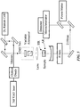
- a hemispherical cavity of the length 19.7 cm was utilized.
- the arrangement depicted in Fig. 7 does not form part of the invention as claimed in the present application but represents additional technical information that is useful for understanding the invention as claimed.
- Wavelength tuning was realized using a CaF 2 Brewster prism as the dispersive element placed 5 cm from the output coupler. The focusing lens and crystal remained at the positions that were used in the nonselective cavity.
- the pump source was operating at 1.5607 ⁇ m with the pulse energy of about 600 ⁇ J and 5 ns pulse duration in a TEM 00 mode. This pump energy was about three times larger than the threshold pump energy level.
- the Cr 2+ :ZnS laser output was directed through a CaF 2 lens to a 0.3 m "SpectraPro" monochromator with a PbS detector for wavelength measurements.
- Fig. 8 demonstrates a continuous wavelength tuning that was realized over the 2.05-2.40 ⁇ m spectral region.
- the output of the chromium laser oscillation had a linewidth of approximately 30 nm (FWHM).
- the peak efficiency of the tunable output was centered at 2.25 ⁇ m.
- the tuning limits were due to coatings of the cavity optics and not the emission spectrum of Cr 2+ :ZnS crystal. The use of proper broadband coatings could potentially increase the tuning range to 1.85-2.7 ⁇ m.
- the laser output linewidth could be further narrowed by means of a Littrow or Littman configured grating tuned cavity.
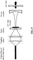
- FIG. 9 A block diagram of experimental set-up for Cr 2+ :ZnS CW lasing under Er fiber laser excitation in external hemispherical cavity is depicted in Fig. 9 .
- Pump source was an Erbium Doped Fiber Laser (ELD-2, IPG Photonics). This laser delivers 2W of single mode CW non-polarized radiation at 1550 nm and was equipped with an optical isolator to prevent any possible feedback from the ZnS and ZnSe laser system.
- the fiber core was 5 ⁇ m in diameter.
- the hemispherical cavity consisted of the flat input mirror and output mirror with 20 cm radius.
- the input mirror crystal had 99.5% reflectivity in the spectral region from 2.2 to 2.5 ⁇ m.
- the output mirrors had either 2-20% transmission in the spectral region 2.2-2.5 ⁇ m, or 20-30% transmission in the spectral region 1.95-2.5 ⁇ m. Both output mirrors had their peak reflectivity at 2.360 ⁇ m.
- the antireflection coated chromium doped ZnS crystal with a thickness of 1.1 mm and an absorption coefficient of 5 cm -1 at the pump wavelength was utilized.
- the crystal was mounted on an optical contact to the input flat dichoric mirror made from the YAG crystal for the sake of effective dissipation of heat.
- the pump radiation of the Er fiber laser was first collimated with a microscope objective in a parallel pencil of light having 1 mm in diameter, and than focused with a second 15 mm focal length objective into the crystal through the input mirror.
- the output laser parameters were different when the cavity was adjusted to minimum threshold and maximum output power.
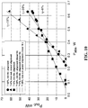
- the output-input dependences for ZnS:Cr 2+ continuous wave lasing under Er fiber pumping for two different output couplers and for different cavity adjustments to the minimum threshold and maximum output power are depicted in Fig. 10 .
- the minimum threshold values were measured to be 100 mW and 200 mW of absorbed pump power for output couplers with 2% and 20% transmission, respectively.
- An output power of 63 mW near 2370 nm at an absorbed pump power of 0.6W was demonstrated with an output coupler with 2% transmission for maximum output power adjustment.
- the maximum slope efficiency " ⁇ " with respect to the absorbed pump power was 18% in this exper A.
- the round trip passive losses "L d " in the cavity were estimated to be of 3.7% from the Findley-Clay analysis.
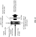
- FIG. 11 A block diagram of Cr 2+ :ZnS and Cr 2 +:ZnSe gain switched microchip lasers with mirrors deposited on the crystal facets is depicted in Fig. 11 .
- the arrangement described in Fig. 11 does not form part of the invention as claimed in the present application but represents additional technical information that is useful for understanding the invention as claimed.
- Gain switched microchip laser experiments were performed with Cr 2+ doped ZnSe and ZnS.
- the crystal used were 0.5-3mm thick with polished but uncoated parallel faces and had coefficient of absorption of k ⁇ 6cm -1 at 1.77 ⁇ m.
- Pumping was from the 1.56 ⁇ m output of a D 2 Raman shifted Nd:YAG operating at 10Hz with a pulse duration of about 5 ns and 1.5mm beam diameter.
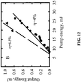
- Output-input energies for pulsed ZnSe microchip lasing for different lasing spots are shown in Fig. 12 .
- Threshold input energy was found to be 7mJ.
- a maximum slope efficiency of 6.5% and maximum output power of 1 mJ were obtained for a microchip without mirrors, when positive feedback was only due to the Fresnel reflections.
- the spectral range of the free-running laser output was from 2270 to-2290nm.
- FIG. 13 A block diagram of experimental set-up for Cr 2+ :ZnS and Cr 2+ :ZnSe CW lasing under Er fiber laser excitation in microchip configuration is displayed in Fig. 13 .
- Cr 2+ :ZnS and Cr 2+ :ZnSe crystals were studied.
- the crystals were polished flat and parallel (parallelism of -10") to 1.1 and 2.5 mm thickness, respectively.
- the mirrors were directly deposited on the parallel polished facets of a thin wafer of laser material.
- Input and output dichroic mirrors had 0.01 and 3.5% transmission over 2300-2500 nm spectral region, respectively, and their transmission at 1550 nm pumping wavelength was 75%. Two different pump arrangements were utilized.
- the first one was identical to the pump conditions for the Cr 2+ :ZnS CW lasing in hemispherical cavity when the pump radiation of the Er fiber laser was first collimated with a microscope objective in a parallel pencil of light having 1 mm in diameter, and then focused with a second 15 mm focal length objective into the crystal through the input mirror.
- the second pump arrangement was provided without any additional optics by means of the microchip laser mounting at a close ( ⁇ 20 um) distance from the tip of the pump Er-fiber laser.
- the rather large value of the temperature derivative of the refraction index for ZnS and ZnSe crystals ( ⁇ 5 times larger than for YAG crystal) played a constructive role by means of creating a strong positive lens and providing effective stabilization of the microchip cavity.
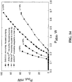
- Fig. 14 shows the output power of the Cr 2+ :ZnS and Cr 2+ :ZnSe microchip laser plotted as a function of absorbed pump power.
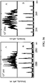
- the output spectrum in free-running laser operation covered the spectrum range from 2280 to 2360 and from 2480 to 2590 for ZnS and ZnSe microchip lasers, respectively.
- L 330 mm from output laser surfaces.
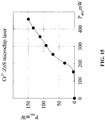
- a 18 mrad FWHM of the intensity profile was measured for the Cr 2+ :ZnS laser. It is slightly less than that for Cr 2+ :ZnSe laser (25 mrad).
- the divergence difference may be explained by a lower dn / dT in Cr 2+ :ZnS crystal (+46x10 -6 K -1 in ZnS vs. +70x10 -6 K -1 in ZnSe).
- the laser operates as follows. Emission from the spatially separated channels of the active medium passes through the intracavity lens into the off-axis mode suppression element, aperture A, which together with the spatially filtered pump radiation divides active zone of the gain waveguide into a number of channels and separates from the amplified emission of individual channel only part of it that is spread parallel to the resonator axis. This separated radiation is diffracted on the diffraction grating.
- the Littrow mount grating works as a retroreflector in the auto-collimating regime in the first order of diffraction and returns part of radiation back to the aperture.
- the off-axis mode suppression element, aperture in turn extracts from the diffracted radiation only the radiation of the main laser modes.
- the aperture should simultaneously select the fundamental transverse modes for all existing channels in the cavity.
- the radiation of the main laser modes, each with a distinct wavelength, is collimated by the focusing lens and directed back to the active medium.
- the optical components of the cavity maintain distinct gain channels in the active zone of active element, reduce cross talk, suppress mode competition, and force each channel to lase at specific stabilized wavelength.
- This approach allows the construction of the laser that emits a plurality of narrow spectral lines that can be easily tailored to any pre-assigned spectral composition within the amplification spectrum of the gain medium.
- TM doped II-VI hosts and, specifically, chromium doped ZnS and ZnSe crystals featuring broad amplification spectra are ideal active media for superbroadband and multiline lasing.
- FIG. 19 displays further chip scale integration of multiline TM:II-VI laser.
- This integrated optical chip is made on II-VI substrate.
- the chip consists of several sections.
- the right section has multiple V-grooves etched in II-VI substrate and is provided for connection with fiber lasers or fiber coupled diode lasers.
- Central section consists of multiple waveguides (e.g. made by ion exchange or ridge technology) and provides delivery of the pump radiation to the active section.
- the active section consists of multiple II-VI waveguides doped with TM 2+ and can be further combined with dispersive element such as a tapered grating. Tapered grating, for example, can be provided by exposing active waveguides with UV interference pattern.
- Utilization of tapered grating provides an autocollimation regime of retroreflection for different wavelengths for each individual active waveguide giving rise to a multifrequency regime of oscillation. Due to electro-optic properties of II-VI materials it is possible to integrate Mach-Zehnder or electro-reflection internal modulator with the active section of the same waveguide (not shown on the Figure). Output multifrequency radiation can be coupled to an output fiber.
Landscapes
- Physics & Mathematics (AREA)
- Electromagnetism (AREA)
- Engineering & Computer Science (AREA)
- Optics & Photonics (AREA)
- Plasma & Fusion (AREA)
- Chemical & Material Sciences (AREA)
- Crystallography & Structural Chemistry (AREA)
- Inorganic Chemistry (AREA)
- Metallurgy (AREA)
- Organic Chemistry (AREA)
- Materials Engineering (AREA)
- Nonlinear Science (AREA)
- Lasers (AREA)
Claims (16)
- Verfahren zum Bauen und Verwenden eines mit einem Übergangsmetall dotierten Lasermediums, umfassend die folgenden Schritte:a. Bilden eines Kristalls mit einer Dicke, die für die Verwendung als ein Mikrochip-Lasermaterial ausreicht, wobei der Kristall ausgewählt ist aus den Strukturen von MeX2Z4 und MeZ, wobei Me ausgewählt ist aus der Gruppe bestehend aus Zn, Cd, Ca, Mg, Sr, Ba, Hg und Pb; Z ausgewählt ist aus der Gruppe bestehend aus S, Se, Te, O und ihren Gemischen; und X ausgewählt ist aus der Gruppe bestehend aus Ga, In und Al;b. Aufbringen einer Dünnfilmschicht aus einem Übergangsmetall auf gegenüberliegenden Flächen des Kristalls durch ein Verfahren, ausgewählt aus der Gruppe aus Laserstrahlverdampfen, Lichtbogenverdampfen und Plasmasputtern;c. Glühen des Kristalls in einem Ofen für einen Zeitraum und bei einer Temperatur, der/die ausreichend ist, um das Dotieren der Übergangsmetallionen in dem Kristall durch Übergangsmetalldiffusion und -austausch in ausgewählten Bereichen des Kristalls zuzulassen, wobei der dotierte Kristall funktionsfähig ist, um Pumplicht mit einer Pumpwellenlänge zu absorbieren, um eine Laserverstärkung mit einer Laserwellenlänge zu erzeugen, die anders als die Pumpwellenlänge ist, dadurch gekennzeichnet, dass es ferner Folgendes umfasst:
Errichten eines elektrischen Felds über den Kristall und zwischen Übergangsmetall-Dünnfilmen auf den gegenüberliegenden Oberflächen des Kristalls während des Glühschritts, um die Übergangsmetalldiffusion zu fördern, und nach dem Glühschritt Aufbringen von zwei dichroitischen Spiegeln jeweils unmittelbar auf zwei gegenüberliegenden Flächen des Kristalls, wobei die zwei dichroitischen Spiegel konfiguriert sind, um Licht mit der Laserwellenlänge auf solche Weise zu reflektieren, um einen Laserhohlraum zwischen den zwei dichroitischen Spiegeln zu bilden und um Licht mit der Pumpwellenlänge zu übermitteln, um Lichtabsorption in dem Kristall zu bewirken, um einen positiven Linseneffekt in dem Kristall zu verursachen, um den Laserhohlraum zu stabilisieren. - Verfahren nach Anspruch 1, ferner gekennzeichnet durch Polieren der Flächen des Kristalls nach dem Dotieren.
- Verfahren nach Anspruch 1, wobei Me ausgewählt ist aus der Gruppe aus Zn und Cd.
- Verfahren nach Anspruch 3, wobei Z ausgewählt ist aus der Gruppe aus S, Se und Te.
- Verfahren nach Anspruch 1, wobei der Kristall ZnS ist und das Übergangsmetall Cr++ ist.
- Verfahren nach Anspruch 1, wobei der Kristall eine Dicke von weniger als etwa 3,0 Millimeter hat.
- Verfahren nach Anspruch 1, wobei der Zeitraum im Bereich von zwischen drei bis zwanzig Tage ist und die Temperatur etwa 830 ° bis etwa 1100 °C ist.
- Verfahren nach Anspruch 1, wobei das Dotieren nur in definierten Bereichen nahe der Flächen des Kristalls auftritt.
- Verfahren nach Anspruch 1, wobei das Dotieren über die Weite des Kristalls variiert wird durch Variieren des Diffusionsgradienten, sodass variierende Konzentrationen von Übergangsmetallsubstitution in dem Kristall erzeugt werden.
- Verfahren nach Anspruch 2, ferner umfassend das Aufbringen von Spiegeln auf den Flächen des Kristalls nach dem Polieren der Flächen des Kristalls.
- Verfahren nach Anspruch 1, ferner umfassend das Aufteilen des Kristalls in eine Vielzahl von Mikrochip-großen Einheiten, die einen TM:MeZ-Wafer mit Spiegeln auf gegenüberliegenden Flächen haben.
- Verfahren nach Anspruch 11, wobei jede Mikrochip-große Einheit in dem TM:MeZ-Wafer einen Dotierungskonzentrationsgradienten definiert hat.
- Verfahren nach Anspruch 1, umfassend das Bereitstellen eines Spiegels, um einen gekoppelten Hohlraum mit den zwei dichroitischen Siegeln zu bilden, um Modi des Lasers zu steuern.
- Verfahren nach Anspruch 11, ferner umfassend das Befestigen von mindestens einem der Mikrochip-großen Einheiten auf einem Halbleiter einschließlich einer Erregerdiode.
- Verfahren nach Anspruch 11, ferner umfassend den Schritt des Bereitstellens von Dauerstrich-Anregungsenergie an den Kristall, um eine Dauerstrichgaslaser-Ausgangsstrahlung anzuregen.
- Verfahren nach Anspruch 11, ferner umfassend das Bereitstellen von gepulster Anregungsenergie an den Kristall, um eine Impulslaser-Ausgangsstrahlung anzuregen.
Applications Claiming Priority (3)
| Application Number | Priority Date | Filing Date | Title |
|---|---|---|---|
| US32355101P | 2001-09-20 | 2001-09-20 | |
| US323551P | 2001-09-20 | ||
| PCT/US2002/029707 WO2003026086A1 (en) | 2001-09-20 | 2002-09-19 | MID-IR MICROCHIP LASER: ZnS:Cr2+ LASER WITH SATURABLE ABSORBER MATERIAL |
Publications (3)
| Publication Number | Publication Date |
|---|---|
| EP1436865A1 EP1436865A1 (de) | 2004-07-14 |
| EP1436865A4 EP1436865A4 (de) | 2005-12-28 |
| EP1436865B1 true EP1436865B1 (de) | 2019-06-05 |
Family
ID=23259696
Family Applications (1)
| Application Number | Title | Priority Date | Filing Date |
|---|---|---|---|
| EP02761727.3A Expired - Lifetime EP1436865B1 (de) | 2001-09-20 | 2002-09-19 | MICROCHIPLASER FÜR DEN MITTLEREN IR-BEREICH: ZnS:Cr-2+-LASER MIT SÄTTIGBAREM ABSORBIERERMATERIAL |
Country Status (6)
| Country | Link |
|---|---|
| US (6) | US6960486B2 (de) |
| EP (1) | EP1436865B1 (de) |
| JP (1) | JP2005504437A (de) |
| CN (1) | CN1589513A (de) |
| CA (2) | CA2783176C (de) |
| WO (1) | WO2003026086A1 (de) |
Families Citing this family (26)
| Publication number | Priority date | Publication date | Assignee | Title |
|---|---|---|---|---|
| US7606274B2 (en) * | 2001-09-20 | 2009-10-20 | The Uab Research Foundation | Mid-IR instrument for analyzing a gaseous sample and method for using the same |
| US8817830B2 (en) * | 2002-09-19 | 2014-08-26 | The Uab Research Foundation | Saturable absorbers for Q-switching of middle infrared laser cavaties |
| EP1436865B1 (de) * | 2001-09-20 | 2019-06-05 | University of Alabama at Birmingham Research Foundation | MICROCHIPLASER FÜR DEN MITTLEREN IR-BEREICH: ZnS:Cr-2+-LASER MIT SÄTTIGBAREM ABSORBIERERMATERIAL |
| US7024066B1 (en) * | 2003-04-07 | 2006-04-04 | Luxtera, Inc. | Littrow gratings as alignment structures for the wafer level testing of optical and optoelectronic chips |
| US7286573B1 (en) | 2004-08-12 | 2007-10-23 | United States Of America As Represented By The Administrator Of The National Aeronautics And Space Administration (Nasa) | Conversion of type of quantum well structure |
| JPWO2007013608A1 (ja) | 2005-07-28 | 2009-02-12 | パナソニック株式会社 | レーザ光源およびディスプレイ装置 |
| US7519253B2 (en) | 2005-11-18 | 2009-04-14 | Omni Sciences, Inc. | Broadband or mid-infrared fiber light sources |
| US10278711B2 (en) * | 2006-02-27 | 2019-05-07 | Biomet Manufacturing, Llc | Patient-specific femoral guide |
| EP2052445A4 (de) * | 2006-03-13 | 2014-05-07 | Uab Research Foundation | Elektrische gepumpte breit abstimmbare infrarot-laser auf der basis quantenbegrenzter übergangsmetalldotierter halbleiter |
| US7995631B2 (en) * | 2006-04-14 | 2011-08-09 | Raytheon Company | Solid-state laser with spatially-tailored active ion concentration using valence conversion with surface masking and method |
| WO2008052161A2 (en) * | 2006-10-27 | 2008-05-02 | University Of Alabama At Birmingham Research Foundation | Saturable absorbers for q-switching of middle infrared laser cavities |
| KR101529367B1 (ko) * | 2008-12-02 | 2015-06-16 | 바이오리텍 파마 마케팅 엘티디. | 레이저 유발 증기/플라스마 매개 의학적 처치방법 및 장치 |
| FR2971640B1 (fr) | 2011-02-16 | 2014-04-04 | Univ Bordeaux 1 | Dispositif de pompage optique. |
| CN102208749B (zh) * | 2011-04-15 | 2012-06-27 | 中国人民解放军国防科学技术大学 | 中、远红外双波段激光器 |
| DE102011054024B4 (de) * | 2011-09-28 | 2014-10-09 | Deutsches Zentrum für Luft- und Raumfahrt e.V. | Infrarotlaserverstärkersystem |
| JPWO2015105154A1 (ja) * | 2014-01-10 | 2017-03-23 | 国立研究開発法人理化学研究所 | 医療用レーザ光源システム |
| CN103897692A (zh) * | 2014-03-31 | 2014-07-02 | 中国科学院上海光学精密机械研究所 | 过渡金属离子浓度渐变掺杂硫化锌或硒化锌及其制备方法 |
| WO2016024877A1 (ru) * | 2014-08-13 | 2016-02-18 | Федеральное государственное бюджетное учреждение науки Институт химии высокочистых веществ им. Г.Г. Девятых Российской академии наук (ИХВВ РАН) | Способ получения легированных халькогенидов цинка |
| US9768901B2 (en) * | 2014-11-20 | 2017-09-19 | Kaiam Corp. | Planar lightwave circuit active connector |
| US10211600B2 (en) * | 2015-03-23 | 2019-02-19 | Ipg Photonics Corporation | High power CW mid-IR laser |
| CN105204115B (zh) * | 2015-10-10 | 2018-02-16 | 浙江大学 | 一种基于对称金属包覆波导的中红外波段可调光延时器 |
| US11067438B2 (en) | 2017-07-27 | 2021-07-20 | Canare Electric Co., Ltd. | Laser beam profile measurement device |
| JP6551898B1 (ja) * | 2017-09-05 | 2019-07-31 | 国立研究開発法人量子科学技術研究開発機構 | レーザー装置、光源および測定装置 |
| CN110082349B (zh) * | 2019-02-01 | 2021-11-02 | 南京师范大学 | 一种基于olci的内陆富营养化湖泊水体蓝藻生物量比例遥感估算方法 |
| US11947048B2 (en) | 2020-05-06 | 2024-04-02 | Waymo Llc | Crosstalk reduction for light detection and ranging (lidar) devices using wavelength locking |
| CN113186602B (zh) * | 2021-04-29 | 2023-06-02 | 杭州光学精密机械研究所 | 一种Cr掺杂II-VI族化合物同质包边多晶激光材料及其制备方法 |
Family Cites Families (42)
| Publication number | Priority date | Publication date | Assignee | Title |
|---|---|---|---|---|
| US3820896A (en) * | 1973-01-02 | 1974-06-28 | Singer Co | Velocimeter with improved signal to noise ratio |
| US4070094A (en) * | 1975-08-25 | 1978-01-24 | The United States Of America As Represented By The Secretary Of The Navy | Optical waveguide interferometer modulator-switch |
| US4097118A (en) * | 1975-10-30 | 1978-06-27 | Rca Corporation | Optical waveguide coupler employing deformed shape fiber-optic core coupling portion |
| US4169009A (en) * | 1977-03-30 | 1979-09-25 | United Technologies Corporation | Large area microstructure processing |
| US4124270A (en) * | 1977-03-30 | 1978-11-07 | United Technologies Corporation | Monolithic, three-dimensional infrared waveguide for high power lasers |
| US4158207A (en) * | 1978-03-27 | 1979-06-12 | The United States Of America As Represented By The Secretary Of The Navy | Iron-doped indium phosphide semiconductor laser |
| US4762382A (en) * | 1987-06-29 | 1988-08-09 | Honeywell Inc. | Optical interconnect circuit for GaAs optoelectronics and Si VLSI/VHSIC |
| US4847138A (en) * | 1987-10-07 | 1989-07-11 | Corning Glass Works | Thermal writing on glass and glass-ceramic substrates |
| US5070488A (en) * | 1988-06-29 | 1991-12-03 | Atsuko Fukushima | Optical integrated circuit and optical apparatus |
| US5022729A (en) * | 1988-10-21 | 1991-06-11 | Sony Corporation | Optical waveguide and second harmonic generator |
| US5009502A (en) * | 1989-04-20 | 1991-04-23 | Hughes Aircraft Company | System of holographic optical elements for testing laser range finders |
| US4991926A (en) * | 1990-04-06 | 1991-02-12 | Litton Systems, Inc. | Integrated optics decorrelator |
| US5488626A (en) * | 1991-01-14 | 1996-01-30 | Light Age, Inc. | Method of and apparatus for pumping of transition metal ion containing solid state lasers using diode laser sources |
| US5321711A (en) * | 1992-08-17 | 1994-06-14 | Alliedsignal Inc. | Segmented solid state laser gain media with gradient doping level |
| US5461635A (en) * | 1993-04-02 | 1995-10-24 | Basiev; Tasoltan T. | Solid state laser with superbroadband or control generation spectrum |
| US5379310A (en) * | 1993-05-06 | 1995-01-03 | Board Of Trustees Of The University Of Illinois | External cavity, multiple wavelength laser transmitter |
| DE4427215A1 (de) * | 1993-08-02 | 1995-02-23 | Agency Ind Science Techn | Transparente und leitfähige ultradünne Filme und Verfahren zu ihrer Herstellung |
| US5428635A (en) * | 1994-01-11 | 1995-06-27 | American Biogenetic Sciences, Inc. | Multi-wavelength tunable laser |
| GB9405613D0 (en) * | 1994-03-22 | 1994-05-11 | British Tech Group | Laser waveguide |
| US5541948A (en) * | 1994-11-28 | 1996-07-30 | The Regents Of The University Of California | Transition-metal doped sulfide, selenide, and telluride laser crystal and lasers |
| AU4144497A (en) * | 1996-05-17 | 1997-12-05 | Uab Research Foundation | Semiconductor laser with a superbroadband or multiline spectral output |
| FR2751480A1 (fr) * | 1996-07-19 | 1998-01-23 | Commissariat Energie Atomique | Microlaser solide a declenchement actif par semi-conducteur |
| US5796771A (en) * | 1996-08-19 | 1998-08-18 | The Regents Of The University Of California | Miniature self-pumped monolithically integrated solid state laser |
| US5832008A (en) * | 1997-01-24 | 1998-11-03 | Hughes Electronics | Eyesafe laser system using transition metal-doped group II-VI semiconductor as a passive saturable absorber Q-switch |
| EP0987769B1 (de) * | 1998-09-18 | 2003-05-02 | Sumitomo Electric Industries, Ltd. | Photodiodenmodul |
| US6330388B1 (en) * | 1999-01-27 | 2001-12-11 | Northstar Photonics, Inc. | Method and apparatus for waveguide optics and devices |
| US6297179B1 (en) * | 1999-10-18 | 2001-10-02 | Corning Incorporated | Transition-metal, glass-ceramic gain media |
| US6326666B1 (en) * | 2000-03-23 | 2001-12-04 | International Business Machines Corporation | DTCMOS circuit having improved speed |
| DE10102818A1 (de) * | 2001-01-23 | 2002-08-08 | Lohmann Therapie Syst Lts | Primärverpackungseinheit für mehrere vereinzelte Filmplättchen als Darreichungsformen |
| CN1313656C (zh) * | 2001-03-02 | 2007-05-02 | 独立行政法人科学技术振兴机构 | Ⅱ-ⅵ族或ⅲ-ⅴ族系单结晶铁磁性化合物及其铁磁性特性的调整方法 |
| AU2002255791A1 (en) * | 2001-03-16 | 2002-10-03 | Peregrine Semiconductor Corporation | Coupled optical and optoelectronic devices, and method of making the same |
| GB2379747B (en) * | 2001-06-22 | 2003-08-27 | Bookham Technology Plc | Optical Chip with optic fibre alignment features |
| EP1436865B1 (de) * | 2001-09-20 | 2019-06-05 | University of Alabama at Birmingham Research Foundation | MICROCHIPLASER FÜR DEN MITTLEREN IR-BEREICH: ZnS:Cr-2+-LASER MIT SÄTTIGBAREM ABSORBIERERMATERIAL |
| US8817830B2 (en) * | 2002-09-19 | 2014-08-26 | The Uab Research Foundation | Saturable absorbers for Q-switching of middle infrared laser cavaties |
| US7606274B2 (en) * | 2001-09-20 | 2009-10-20 | The Uab Research Foundation | Mid-IR instrument for analyzing a gaseous sample and method for using the same |
| US7672546B2 (en) * | 2001-10-09 | 2010-03-02 | Infinera Corporation | Optical transport network having a plurality of monolithic photonic integrated circuit semiconductor chips |
| US7751658B2 (en) * | 2001-10-09 | 2010-07-06 | Infinera Corporation | Monolithic transmitter photonic integrated circuit (TxPIC) having tunable modulated sources with feedback system for source power level or wavelength tuning |
| EP1436870A2 (de) * | 2001-10-09 | 2004-07-14 | Infinera Corporation | Integrierte fotonische sendschaltung und optisches netzwerk damit |
| US7194016B2 (en) * | 2002-03-22 | 2007-03-20 | The Research Foundation Of The University Of Central Florida | Laser-to-fiber coupling |
| WO2005003845A2 (en) | 2003-02-03 | 2005-01-13 | Bae Systems Information And Electronic Systems Integration Inc. | Method and apparatus for generating mid and long ir wavelength radiation |
| US8288157B2 (en) * | 2007-09-12 | 2012-10-16 | Plc Diagnostics, Inc. | Waveguide-based optical scanning systems |
| US7676122B2 (en) * | 2006-12-11 | 2010-03-09 | Jiahua James Dou | Apparatus, system and method for particle manipulation using waveguides |
-
2002
- 2002-09-19 EP EP02761727.3A patent/EP1436865B1/de not_active Expired - Lifetime
- 2002-09-19 US US10/247,272 patent/US6960486B2/en not_active Expired - Lifetime
- 2002-09-19 CA CA2783176A patent/CA2783176C/en not_active Expired - Lifetime
- 2002-09-19 JP JP2003529589A patent/JP2005504437A/ja active Pending
- 2002-09-19 WO PCT/US2002/029707 patent/WO2003026086A1/en not_active Ceased
- 2002-09-19 CA CA2461096A patent/CA2461096C/en not_active Expired - Lifetime
- 2002-09-19 CN CNA028229487A patent/CN1589513A/zh active Pending
-
2005
- 2005-05-27 US US11/140,271 patent/US7548571B2/en not_active Expired - Lifetime
-
2009
- 2009-06-16 US US12/485,826 patent/US20100022049A1/en not_active Abandoned
-
2011
- 2011-12-01 US US13/309,496 patent/US8767789B2/en not_active Expired - Lifetime
-
2014
- 2014-07-01 US US14/321,553 patent/US9887510B2/en not_active Expired - Fee Related
-
2018
- 2018-01-30 US US15/884,271 patent/US20180175579A1/en not_active Abandoned
Non-Patent Citations (1)
| Title |
|---|
| LESCROART G ET AL: "Experimental investigations and theoretical modeling of a Tm:YVO4 microchip laser", OPTICS COMMUNICATIONS, NORTH-HOLLAND PUBLISHING CO. AMSTERDAM, NL, vol. 143, no. 1-3, 1 November 1997 (1997-11-01), pages 147 - 155, XP004094030, ISSN: 0030-4018, DOI: 10.1016/S0030-4018(97)00302-7 * |
Also Published As
| Publication number | Publication date |
|---|---|
| US9887510B2 (en) | 2018-02-06 |
| US20120224599A1 (en) | 2012-09-06 |
| US8767789B2 (en) | 2014-07-01 |
| US7548571B2 (en) | 2009-06-16 |
| EP1436865A4 (de) | 2005-12-28 |
| US6960486B2 (en) | 2005-11-01 |
| CA2783176A1 (en) | 2003-03-27 |
| CA2461096C (en) | 2014-02-18 |
| CA2461096A1 (en) | 2003-03-27 |
| US20150333470A1 (en) | 2015-11-19 |
| CA2783176C (en) | 2014-05-20 |
| US20180175579A1 (en) | 2018-06-21 |
| US20100022049A1 (en) | 2010-01-28 |
| CN1589513A (zh) | 2005-03-02 |
| JP2005504437A (ja) | 2005-02-10 |
| US20050281301A1 (en) | 2005-12-22 |
| WO2003026086A1 (en) | 2003-03-27 |
| EP1436865A1 (de) | 2004-07-14 |
| US20030072340A1 (en) | 2003-04-17 |
Similar Documents
| Publication | Publication Date | Title |
|---|---|---|
| US9887510B2 (en) | Mid-IR microchip laser: ZnS:Cr2+ laser with saturable absorber material | |
| Vodopyanov | Laser-based mid-infrared sources and applications | |
| Fedorov et al. | 3.77-5.05-μm tunable solid-state lasers based on Fe/sup 2+/-doped ZnSe crystals operating at low and room temperatures | |
| Mirov et al. | Progress in mid-IR lasers based on Cr and Fe-doped II–VI chalcogenides | |
| Sorokin et al. | Ultrabroadband infrared solid-state lasers | |
| Tsuda et al. | Mode-locking ultrafast solid-state lasers with saturable Bragg reflectors | |
| Mirov et al. | Recent progress in transition-metal-doped II–VI Mid-IR lasers | |
| Agnesi et al. | Optical spectroscopy and diode-pumped laser performance of Nd/sup 3+/in the CNGG crystal | |
| Carrig | Transition-metal-doped chalcogenide lasers | |
| Akimov et al. | Efficient IR Fe: ZnSe laser continuously tunable in the spectral range from 3.77 to 4.40 μm | |
| Carrig et al. | Chromium-doped chalcogenide lasers | |
| Mirov et al. | Diode and fibre pumped Cr2+: ZnS mid-infrared external cavity and microchip lasers | |
| US20140362879A1 (en) | Saturable absorbers for q-switching of middle infrared laser cavaties | |
| Sorokina | Broadband mid-infrared solid-state lasers | |
| Graham et al. | Spectroscopic characterization and laser performance of diffusion doped Cr2+: ZnS | |
| Graham et al. | Pulsed mid-IR Cr2+: ZnS and Cr2+: ZnSe lasers pumped by Raman-shifted Q-switched neodymium lasers | |
| Kück | Spectroscopy and laser characteristics of Cr2+-doped chalcogenide crystals—overview and recent results | |
| McKinnie et al. | Ti/sup 3+/ion concentration and Ti: sapphire laser performance | |
| Graham et al. | Laser performance of Cr2+-doped ZnS | |
| Mond et al. | Continuous wave diode pumped Cr2+: ZnSe and high power laser operation | |
| Basiev et al. | Colour centre lasers | |
| Wagner et al. | High-efficiency, broadly tunable continuous-wave Cr2+: ZnSe laser | |
| Fedorov et al. | Energy scaling of nanosecond gain-switched Cr2+: ZnSe lasers | |
| Doroshenko et al. | Bulk Fe: ZnSe laser gain-switched by the Q-switched Er: YAG laser | |
| Mirov et al. | Progress in Cr and Fe doped ZnSe and ZnS polycrystalline materials and lasers |
Legal Events
| Date | Code | Title | Description |
|---|---|---|---|
| PUAI | Public reference made under article 153(3) epc to a published international application that has entered the european phase |
Free format text: ORIGINAL CODE: 0009012 |
|
| 17P | Request for examination filed |
Effective date: 20040415 |
|
| AK | Designated contracting states |
Kind code of ref document: A1 Designated state(s): AT BE BG CH CY CZ DE DK EE ES FI FR GB GR IE IT LI LU MC NL PT SE SK TR |
|
| AX | Request for extension of the european patent |
Extension state: AL LT LV MK RO SI |
|
| RIN1 | Information on inventor provided before grant (corrected) |
Inventor name: MIROV, SERGEY, B. Inventor name: FEDEROV, VLADIMIR, V. |
|
| A4 | Supplementary search report drawn up and despatched |
Effective date: 20051115 |
|
| 17Q | First examination report despatched |
Effective date: 20080430 |
|
| STAA | Information on the status of an ep patent application or granted ep patent |
Free format text: STATUS: EXAMINATION IS IN PROGRESS |
|
| GRAP | Despatch of communication of intention to grant a patent |
Free format text: ORIGINAL CODE: EPIDOSNIGR1 |
|
| STAA | Information on the status of an ep patent application or granted ep patent |
Free format text: STATUS: GRANT OF PATENT IS INTENDED |
|
| RIC1 | Information provided on ipc code assigned before grant |
Ipc: H01S 3/0941 20060101ALI20181207BHEP Ipc: H01S 3/1055 20060101ALI20181207BHEP Ipc: H01S 3/16 20060101AFI20181207BHEP Ipc: H01S 3/06 20060101ALI20181207BHEP Ipc: H01S 3/117 20060101ALI20181207BHEP Ipc: C30B 31/00 20060101ALI20181207BHEP Ipc: H01S 3/094 20060101ALI20181207BHEP Ipc: C30B 29/48 20060101ALI20181207BHEP Ipc: C30B 31/02 20060101ALI20181207BHEP Ipc: H01S 3/115 20060101ALI20181207BHEP Ipc: H01S 3/113 20060101ALI20181207BHEP Ipc: H01S 3/00 20060101ALI20181207BHEP Ipc: H01S 3/108 20060101ALI20181207BHEP Ipc: H01S 3/08 20060101ALI20181207BHEP |
|
| INTG | Intention to grant announced |
Effective date: 20190104 |
|
| RIC1 | Information provided on ipc code assigned before grant |
Ipc: C30B 31/00 20060101ALI20181207BHEP Ipc: C30B 29/48 20060101ALI20181207BHEP Ipc: H01S 3/115 20060101ALI20181207BHEP Ipc: H01S 3/0941 20060101ALI20181207BHEP Ipc: H01S 3/117 20060101ALI20181207BHEP Ipc: C30B 31/02 20060101ALI20181207BHEP Ipc: H01S 3/094 20060101ALI20181207BHEP Ipc: H01S 3/16 20060101AFI20181207BHEP Ipc: H01S 3/06 20060101ALI20181207BHEP Ipc: H01S 3/1055 20060101ALI20181207BHEP Ipc: H01S 3/00 20060101ALI20181207BHEP Ipc: H01S 3/113 20060101ALI20181207BHEP Ipc: H01S 3/08 20060101ALI20181207BHEP Ipc: H01S 3/108 20060101ALI20181207BHEP |
|
| GRAS | Grant fee paid |
Free format text: ORIGINAL CODE: EPIDOSNIGR3 |
|
| GRAA | (expected) grant |
Free format text: ORIGINAL CODE: 0009210 |
|
| STAA | Information on the status of an ep patent application or granted ep patent |
Free format text: STATUS: THE PATENT HAS BEEN GRANTED |
|
| AK | Designated contracting states |
Kind code of ref document: B1 Designated state(s): AT BE BG CH CY CZ DE DK EE ES FI FR GB GR IE IT LI LU MC NL PT SE SK TR |
|
| REG | Reference to a national code |
Ref country code: GB Ref legal event code: FG4D |
|
| REG | Reference to a national code |
Ref country code: CH Ref legal event code: EP |
|
| REG | Reference to a national code |
Ref country code: AT Ref legal event code: REF Ref document number: 1140945 Country of ref document: AT Kind code of ref document: T Effective date: 20190615 |
|
| REG | Reference to a national code |
Ref country code: DE Ref legal event code: R096 Ref document number: 60249923 Country of ref document: DE |
|
| REG | Reference to a national code |
Ref country code: IE Ref legal event code: FG4D |
|
| REG | Reference to a national code |
Ref country code: NL Ref legal event code: MP Effective date: 20190605 |
|
| PG25 | Lapsed in a contracting state [announced via postgrant information from national office to epo] |
Ref country code: SE Free format text: LAPSE BECAUSE OF FAILURE TO SUBMIT A TRANSLATION OF THE DESCRIPTION OR TO PAY THE FEE WITHIN THE PRESCRIBED TIME-LIMIT Effective date: 20190605 Ref country code: ES Free format text: LAPSE BECAUSE OF FAILURE TO SUBMIT A TRANSLATION OF THE DESCRIPTION OR TO PAY THE FEE WITHIN THE PRESCRIBED TIME-LIMIT Effective date: 20190605 Ref country code: FI Free format text: LAPSE BECAUSE OF FAILURE TO SUBMIT A TRANSLATION OF THE DESCRIPTION OR TO PAY THE FEE WITHIN THE PRESCRIBED TIME-LIMIT Effective date: 20190605 |
|
| PG25 | Lapsed in a contracting state [announced via postgrant information from national office to epo] |
Ref country code: GR Free format text: LAPSE BECAUSE OF FAILURE TO SUBMIT A TRANSLATION OF THE DESCRIPTION OR TO PAY THE FEE WITHIN THE PRESCRIBED TIME-LIMIT Effective date: 20190906 Ref country code: BG Free format text: LAPSE BECAUSE OF FAILURE TO SUBMIT A TRANSLATION OF THE DESCRIPTION OR TO PAY THE FEE WITHIN THE PRESCRIBED TIME-LIMIT Effective date: 20190905 |
|
| REG | Reference to a national code |
Ref country code: AT Ref legal event code: MK05 Ref document number: 1140945 Country of ref document: AT Kind code of ref document: T Effective date: 20190605 |
|
| PG25 | Lapsed in a contracting state [announced via postgrant information from national office to epo] |
Ref country code: AT Free format text: LAPSE BECAUSE OF FAILURE TO SUBMIT A TRANSLATION OF THE DESCRIPTION OR TO PAY THE FEE WITHIN THE PRESCRIBED TIME-LIMIT Effective date: 20190605 Ref country code: EE Free format text: LAPSE BECAUSE OF FAILURE TO SUBMIT A TRANSLATION OF THE DESCRIPTION OR TO PAY THE FEE WITHIN THE PRESCRIBED TIME-LIMIT Effective date: 20190605 Ref country code: PT Free format text: LAPSE BECAUSE OF FAILURE TO SUBMIT A TRANSLATION OF THE DESCRIPTION OR TO PAY THE FEE WITHIN THE PRESCRIBED TIME-LIMIT Effective date: 20191007 Ref country code: CZ Free format text: LAPSE BECAUSE OF FAILURE TO SUBMIT A TRANSLATION OF THE DESCRIPTION OR TO PAY THE FEE WITHIN THE PRESCRIBED TIME-LIMIT Effective date: 20190605 Ref country code: NL Free format text: LAPSE BECAUSE OF FAILURE TO SUBMIT A TRANSLATION OF THE DESCRIPTION OR TO PAY THE FEE WITHIN THE PRESCRIBED TIME-LIMIT Effective date: 20190605 Ref country code: SK Free format text: LAPSE BECAUSE OF FAILURE TO SUBMIT A TRANSLATION OF THE DESCRIPTION OR TO PAY THE FEE WITHIN THE PRESCRIBED TIME-LIMIT Effective date: 20190605 |
|
| PG25 | Lapsed in a contracting state [announced via postgrant information from national office to epo] |
Ref country code: IT Free format text: LAPSE BECAUSE OF FAILURE TO SUBMIT A TRANSLATION OF THE DESCRIPTION OR TO PAY THE FEE WITHIN THE PRESCRIBED TIME-LIMIT Effective date: 20190605 |
|
| REG | Reference to a national code |
Ref country code: DE Ref legal event code: R097 Ref document number: 60249923 Country of ref document: DE |
|
| PG25 | Lapsed in a contracting state [announced via postgrant information from national office to epo] |
Ref country code: TR Free format text: LAPSE BECAUSE OF FAILURE TO SUBMIT A TRANSLATION OF THE DESCRIPTION OR TO PAY THE FEE WITHIN THE PRESCRIBED TIME-LIMIT Effective date: 20190605 |
|
| PLBE | No opposition filed within time limit |
Free format text: ORIGINAL CODE: 0009261 |
|
| STAA | Information on the status of an ep patent application or granted ep patent |
Free format text: STATUS: NO OPPOSITION FILED WITHIN TIME LIMIT |
|
| PG25 | Lapsed in a contracting state [announced via postgrant information from national office to epo] |
Ref country code: DK Free format text: LAPSE BECAUSE OF FAILURE TO SUBMIT A TRANSLATION OF THE DESCRIPTION OR TO PAY THE FEE WITHIN THE PRESCRIBED TIME-LIMIT Effective date: 20190605 |
|
| 26N | No opposition filed |
Effective date: 20200306 |
|
| PG25 | Lapsed in a contracting state [announced via postgrant information from national office to epo] |
Ref country code: MC Free format text: LAPSE BECAUSE OF FAILURE TO SUBMIT A TRANSLATION OF THE DESCRIPTION OR TO PAY THE FEE WITHIN THE PRESCRIBED TIME-LIMIT Effective date: 20190605 |
|
| REG | Reference to a national code |
Ref country code: CH Ref legal event code: PL |
|
| PG25 | Lapsed in a contracting state [announced via postgrant information from national office to epo] |
Ref country code: CH Free format text: LAPSE BECAUSE OF NON-PAYMENT OF DUE FEES Effective date: 20190930 Ref country code: IE Free format text: LAPSE BECAUSE OF NON-PAYMENT OF DUE FEES Effective date: 20190919 Ref country code: LU Free format text: LAPSE BECAUSE OF NON-PAYMENT OF DUE FEES Effective date: 20190919 Ref country code: LI Free format text: LAPSE BECAUSE OF NON-PAYMENT OF DUE FEES Effective date: 20190930 |
|
| REG | Reference to a national code |
Ref country code: BE Ref legal event code: MM Effective date: 20190930 |
|
| PG25 | Lapsed in a contracting state [announced via postgrant information from national office to epo] |
Ref country code: BE Free format text: LAPSE BECAUSE OF NON-PAYMENT OF DUE FEES Effective date: 20190930 |
|
| PG25 | Lapsed in a contracting state [announced via postgrant information from national office to epo] |
Ref country code: FR Free format text: LAPSE BECAUSE OF NON-PAYMENT OF DUE FEES Effective date: 20190930 |
|
| PG25 | Lapsed in a contracting state [announced via postgrant information from national office to epo] |
Ref country code: CY Free format text: LAPSE BECAUSE OF FAILURE TO SUBMIT A TRANSLATION OF THE DESCRIPTION OR TO PAY THE FEE WITHIN THE PRESCRIBED TIME-LIMIT Effective date: 20190605 |
|
| PGFP | Annual fee paid to national office [announced via postgrant information from national office to epo] |
Ref country code: GB Payment date: 20210927 Year of fee payment: 20 Ref country code: DE Payment date: 20210929 Year of fee payment: 20 |
|
| REG | Reference to a national code |
Ref country code: DE Ref legal event code: R071 Ref document number: 60249923 Country of ref document: DE |
|
| REG | Reference to a national code |
Ref country code: GB Ref legal event code: PE20 Expiry date: 20220918 |
|
| PG25 | Lapsed in a contracting state [announced via postgrant information from national office to epo] |
Ref country code: GB Free format text: LAPSE BECAUSE OF EXPIRATION OF PROTECTION Effective date: 20220918 |