EP1435677A2 - Elektrischer Verbinder und elektrische oder elektronische Baugruppe mit elektrischem Verbinder - Google Patents
Elektrischer Verbinder und elektrische oder elektronische Baugruppe mit elektrischem Verbinder Download PDFInfo
- Publication number
- EP1435677A2 EP1435677A2 EP03030013A EP03030013A EP1435677A2 EP 1435677 A2 EP1435677 A2 EP 1435677A2 EP 03030013 A EP03030013 A EP 03030013A EP 03030013 A EP03030013 A EP 03030013A EP 1435677 A2 EP1435677 A2 EP 1435677A2
- Authority
- EP
- European Patent Office
- Prior art keywords
- electrical
- circuit board
- busbar
- contact
- connection section
- Prior art date
- Legal status (The legal status is an assumption and is not a legal conclusion. Google has not performed a legal analysis and makes no representation as to the accuracy of the status listed.)
- Granted
Links
Images

Classifications
-
- H—ELECTRICITY
- H01—ELECTRIC ELEMENTS
- H01R—ELECTRICALLY-CONDUCTIVE CONNECTIONS; STRUCTURAL ASSOCIATIONS OF A PLURALITY OF MUTUALLY-INSULATED ELECTRICAL CONNECTING ELEMENTS; COUPLING DEVICES; CURRENT COLLECTORS
- H01R12/00—Structural associations of a plurality of mutually-insulated electrical connecting elements, specially adapted for printed circuits, e.g. printed circuit boards [PCB], flat or ribbon cables, or like generally planar structures, e.g. terminal strips, terminal blocks; Coupling devices specially adapted for printed circuits, flat or ribbon cables, or like generally planar structures; Terminals specially adapted for contact with, or insertion into, printed circuits, flat or ribbon cables, or like generally planar structures
- H01R12/70—Coupling devices
- H01R12/7088—Arrangements for power supply
-
- H—ELECTRICITY
- H01—ELECTRIC ELEMENTS
- H01R—ELECTRICALLY-CONDUCTIVE CONNECTIONS; STRUCTURAL ASSOCIATIONS OF A PLURALITY OF MUTUALLY-INSULATED ELECTRICAL CONNECTING ELEMENTS; COUPLING DEVICES; CURRENT COLLECTORS
- H01R12/00—Structural associations of a plurality of mutually-insulated electrical connecting elements, specially adapted for printed circuits, e.g. printed circuit boards [PCB], flat or ribbon cables, or like generally planar structures, e.g. terminal strips, terminal blocks; Coupling devices specially adapted for printed circuits, flat or ribbon cables, or like generally planar structures; Terminals specially adapted for contact with, or insertion into, printed circuits, flat or ribbon cables, or like generally planar structures
- H01R12/70—Coupling devices
- H01R12/71—Coupling devices for rigid printing circuits or like structures
- H01R12/712—Coupling devices for rigid printing circuits or like structures co-operating with the surface of the printed circuit or with a coupling device exclusively provided on the surface of the printed circuit
- H01R12/716—Coupling device provided on the PCB
-
- H—ELECTRICITY
- H05—ELECTRIC TECHNIQUES NOT OTHERWISE PROVIDED FOR
- H05K—PRINTED CIRCUITS; CASINGS OR CONSTRUCTIONAL DETAILS OF ELECTRIC APPARATUS; MANUFACTURE OF ASSEMBLAGES OF ELECTRICAL COMPONENTS
- H05K1/00—Printed circuits
- H05K1/02—Details
- H05K1/0213—Electrical arrangements not otherwise provided for
- H05K1/0263—High current adaptations, e.g. printed high current conductors or using auxiliary non-printed means; Fine and coarse circuit patterns on one circuit board
Definitions
- the present invention relates to an electrical connector for attachment on a circuit board as well as an electrical or electronic Assembly with a printed circuit board, at least partially arranged thereon electrical or electronic circuit and one on the Printed circuit board attached electrical connector.
- Corresponding modules are for this provided that a circuit arranged on a circuit board have with a connector held on the circuit board connected is.
- the circuit is on the circuit board via this connector on the one hand with a voltage or current source and on the other others with appropriate power supplies to the electrical Connectable to consumers. You can also use the connector Control lines are connected to the circuit.
- the electronic circuit on the circuit board usually includes electrical and / or electronic switching elements, by means of which the comparatively high currents depending on the electrical consumers of control signals on the control lines are switchable.
- the Currents to the consumers and thus also to the circuit Total current are compared to that supplied via the control lines Tax flows large.
- the high currents leading connections of the electrical and / or electronic switching elements must therefore corresponding thick and / or wide conductor tracks with corresponding Contacts of the connector attached to the circuit board connected to be the comparatively high currents with little loss and only a small heat load between the connector and lead the circuit.
- the present invention is therefore based on the object of an electrical or electronic assembly with a circuit board, one on it at least partially arranged electrical or electronic circuit and an electrical connector attached to the circuit board to provide suitable for guiding consumption flows Connections are easy to make, as well as a usable To create connectors.
- the connector according to the invention for fastening on a printed circuit board, on the at least partially an electrical or electronic circuit is arranged, and for the electrical connection of electrical lines with the electrical or electronic circuit includes one on the circuit board attachable housing and an at least partially in or arranged on the housing and connectable with an electrical line Busbar, which has a connection section, wherein, when the connector is attached to the circuit board, the connection section on a surface of the circuit board or from the surface spaced so that at least one contact of an electrical or electronic component of the circuit with the connection section is connectable.
- the electrical or electronic assembly according to the invention comprises a printed circuit board, an electrical one at least partially arranged thereon or electronic circuit and one attached to the circuit board electrical connector according to the invention, wherein at least one electrical or electronic component of the circuit with the connection section the conductor rail and a conductor track on the circuit board is electrically connected.
- the circuit board can be any circuit board act on the electrical or electronic components attachable are.
- printed circuit boards with printed conductor tracks usual thickness and width can be used, however, is fundamental the use of other conductor tracks is also conceivable.
- the electrical or electronic circuit is at least partially open arranged on the circuit board and can in particular be electrical or electronic Have components by means of which currents to electrical Consumers are switchable and at least partially via conductor tracks can be electrically connected on the circuit board.
- the connector according to the invention is used to connect the circuit to corresponding external lines. It has a housing on the PCB is attachable.
- the type of attachment can basically take place conventionally, in particular corresponding connecting elements can be used for this purpose for a snap, snap or screw connection be provided, then corresponding complementary on the circuit board Elements are provided.
- the housing can also be opened glued to the circuit board or by means of contact elements on the PCB are soldered, be attached to it.
- At least one is for guiding currents to electrical consumers conductor rail partially arranged in or on the housing, which, in particular, are made of a material which is a good electrical conductor for example copper or a copper alloy. On the one hand, this can be connected to at least one electrical line, via which a corresponding supply current can be supplied.
- the busbar has a connection section which, when the connector is attached to the circuit board, on a surface the circuit board or spaced from the surface.
- the arrangement is such that at least one contact of an electrical or electronic component of the circuit with the connection section is connectable.
- At least a section of a surface the connecting section is therefore, preferably outside of a Housing of the electrical connector, arranged so that a direct Contacting the section is possible.
- the electrical or electronic component simply with a large one Supply current can be supplied without being wide and / or thick Conductor tracks on the circuit board would be necessary.
- the connection section spaced from the surface there is the possibility the circuit board also in an area between the surface and to print the connecting section with further conductor tracks, so that the circuit board can take up a smaller area overall.
- the connector according to the invention enables production an electrical or electronic assembly according to the invention, at of the at least one electrical or electronic component Circuit with the connection section of the busbar and a conductor track on the circuit board, in particular with another component the circuit or a contact of the electrical connector can be connected, is electrically connected.
- it can in the electrical connection of the conductor track on the circuit board a control line for the electrical or electronic component act if this, for example, an electronic component for Switching of currents is.
- the busbar is preferably used to carry currents that can assume great strengths compared to control currents.
- at least the connection section has a cross-sectional area of at least 1 mm 2 .
- the cross-sectional area is oriented essentially orthogonally to the direction of a current through the connection section.
- connection section of the busbar a carrier for forms the electrical or electronic component.
- the component on the connection section for example, by a Adhesion and / or the electrical connection of the component with the Connection section, for example a solder connection, may be attached.
- the connecting section particularly preferably points to this a thickness of more than 0.2 mm.
- the thickness refers to one Direction in which the component is held on the connection section is, i.e. a perpendicular to a corresponding surface of the connection section. In this way, sufficient stability of the Connection section can be reached.
- the electrical connector according to the invention only has the busbar.
- the Electrical connector according to the invention at least one contact element for the electrical connection of a conductor track and / or one with the Conductor electrically connected contact area with at least has one of the electrical lines.
- the electrical according to the invention The connector can then not only be used to feed or discharge also serve larger currents for electrical consumers, but also for the supply of, for example, control signals to the the circuit board at least partially arranged electronic circuit.
- the contact element can be in itself at a contacting end can be designed in any way so that it with one of the conductor tracks is connectable.
- the contacting end can be used as a contact surface or resilient contact section that only on a corresponding Conductor or contact surface is pressed onto the circuit board his.
- the contact element for insertion into a corresponding opening in the circuit board The insertion direction is formed, and that the connection section of the Busbar oriented substantially orthogonal to the direction of insertion is.
- a corresponding one according to the invention on the printed circuit board electrical connector is attached, the contact element inserted into a corresponding opening in the circuit board and soldered there and that the connection section of the busbar essentially is oriented orthogonal to the direction of insertion.
- the direction of insertion essentially relative to a reference direction of a Contacting end defined on the contact element.
- the contact end can in particular be a pin-like or tongue-like design, have to be inserted into the opening in the circuit board, so that then the direction of insertion parallel to the pin or tongue-shaped Section is oriented.
- connection section Under the orientation of the connection section for the direction of insertion is understood in the case of a linear connection section, that this is essentially orthogonal to the direction of insertion is arranged.
- connection section can also essentially lying in one plane, but non-linear, then the essentially orthogonal orientation is understood that a plane by the extension of the connector section is defined, is oriented perpendicular to the direction of insertion. It can particularly preferably the connection section parallel to the surface the PCB be aligned when the connector is on the PCB is attached. In this way, several can be used independently switching electrical consumers through only one electronic assembly be powered with only one connector.
- the busbar is preferably used to supply a supply current to the electrical circuit. To the individual consumers then, however, currents of similar size may be discharged. It it is therefore preferred that at least one contact element is provided, the one located near the connection section of the busbar Has contact section, so that an electrical or electronic Component electrically with the connection section of the busbar and the contact section is connectable. In particular, the contact section run essentially parallel to the connection section. Such a contact element is therefore of a different type than the aforementioned contact element.
- the contact section can preferably at a free end of the contact element, in particular as Pin or particularly preferably be designed as a contact tongue. On the wider area of the contact tongue is a corresponding connection of the corresponding electrical or electronic component with the Contact tongue particularly easy to manufacture.
- the contact element can preferably end to form a connection be formed with an electrical line.
- a corresponding connector is attached to the circuit board, and that the electrical or electronic component is electrical with both the connection section of the busbar and the contact section connected is. In this way, the supply flows in a level above the circuit board with very little Losses are caused, so that on the circuit board wide and / or thick conductor tracks can be largely avoided, which the Manufacture of the printed circuit board simplified and its size reduced.
- connection section the busbar have a corresponding size. It is then preferred that the connection section of the busbar is bow-shaped is trained. The connection section can thus at both ends or are held in the housing of the electrical connector, whereby overall a very stable arrangement results. Such Busbar can therefore very well as a carrier for the electrical or serve electronic component. In addition, a corresponding Voltage is applied to both ends of the busbar, so that voltage drops across the busbar even at longer lengths are easier to balance.
- the then bow-shaped is particularly preferred Connection section oriented parallel to the circuit board.
- the busbar can in principle at least partially in any or be held on the housing.
- the Busbar only in corresponding channels in or on the housing is pressed in or pressed in.
- the contact elements can accordingly be pressed or pressed into the housing.
- the housing is an injection molded part and that the busbar is at least partially injected into the housing. To this This results in a particularly stable mounting of the busbar or in the housing, with moreover also more complex shaped Busbars, in particular in an area in which these with a electrical line are connectable, can be introduced into the housing.
- the busbar and the contact elements by punching process with the following bending if necessary getting produced.
- the electrical connector can be designed such that the electrical lines cannot be detached from the busbar or, if necessary further contact elements in the connector can be connected, where "insoluble” is understood to mean that to separate the connection Tools or atypical large forces for normal use and / or temperatures are necessary.
- the ends be designed for soldered connections or as an insulation displacement terminal.
- the connector is designed as a plug connector and the busbar and / or the contact element with a plug contact element connected or formed at one end as a plug contact are.
- the busbar and / or the contact element in one piece with the plug contact arranged at one end be trained.
- the electrical or electronic Assembly manufactured independently of the wiring and for example be installed in a vehicle, but only at a later stage the electrical connections simply by making a plug connection can be produced with a complementary connector.
- the housing of the connector according to the invention be designed to produce a plug connection and corresponding Have guide elements.
- electrical or electronic components with the busbar are electrically connectable, basically any electrical or electronic components, in particular electrical or electronic Switches.
- This can be, in particular integrated circuits act in an appropriate IC package are packed.
- electrically connected electrical or electronic component is unpackaged integrated circuit.
- Such components are also referred to as "bare dies”. Since such components are very small, can achieved a particularly compact structure of the electrical assembly become.
- Protective layer can be applied, in particular using corresponding lacquers or gels, in particular self-healing Gels, for example based on silicone gels, can be produced.
- the components can be contacted normally Have designs, but there can also be components for flip-chip contacting be used.
- 1 to 3 comprises an electronic assembly 10 according to one preferred embodiment of the invention, a printed circuit board 12, a attached electrical connector 14, several, in the example four integrated circuits 16 arranged on the plug connector 14, a circuit block 18 formed on the printed circuit board 12 and on the printed circuit board 12 formed conductor tracks 20, which are the integrated circuits 16 connect to circuit block 18.
- the printed circuit board 12 is a conventional printed circuit board, the bores 22 for through-plating, i.e. for holding contact elements, in particular contact pins, from which in conventional, not shown in the figures, printed on the printed circuit board 12 Conductor tracks with a thickness of approximately 35 ⁇ m to the circuit block 18 lead. These conductor tracks can be on one or both sides on the Printed circuit board 12 may be formed.
- the conductor tracks which are also conventionally printed on the printed circuit board 12 20 with a thickness of 35 ⁇ m end in contacting areas 24, on which connections of the integrated circuits 16 for contacting are solderable.
- circuit block 18 is shown only roughly schematically in the figures and can include a variety of electronic components.
- circuit block 18 includes a microprocessor that serves to control the integrated circuits 16.
- the Circuit block 18 continues to have corresponding inputs and outputs are connected to the conductor tracks 20.
- the circuit block 18 forms together with the over the conductor tracks 20 connected integrated circuits 16 an electronic circuit the electronic assembly 10, by means of which four different Consumers can be controlled independently of one another.
- the connector 14 is used to connect electrical lines to the electronic assembly 10 and is on the circuit board 12 by means of the Figures not shown locking elements on also not in the figures complementary locking elements shown held on the circuit board 12.
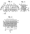
- the connector 14 is shown in more detail in FIGS. 4 to 6.
- the connector 14 comprises a cuboid housing in the example 26 made of plastic, which is manufactured by injection molding.
- the housing has a surface referred to below as the underside 28, with which the housing 26 rests on the circuit board 12 when it is on this is attached.
- the housing 26 comprises an adjoining the underside 28 Side surface, which is referred to below as plug side 30, a circumferential collar 32 on which a guide and receptacle for a corresponding part of an external, not shown in the figures Lines or cables connected complementary connector forms in a plug-in direction parallel to the circuit board 12 in the connector 14 is pluggable.
- first contact elements 34 In the housing 26 there are several, in the example six, first contact elements 34, several, in the example four, second contact elements 36 and one Busbar 38 arranged.
- the first contact elements 34 are in a direction parallel to that Bottom 28 arranged at equal intervals and parallel to each other.
- the one-piece first contact elements 34 each have two sections oriented essentially at right angles to one another (see FIGS. 2 and 5), one of which is designed as a first plug contact tongue Section 40 has a substantially flat, rectangular cross-section and partially on the connector side 30 within the collar 32 out of the housing 26 in a direction parallel to the printed circuit board 12 protrudes so that it is the first plug-in contact tongue 40 for a plug connection with a corresponding contact sleeve of the complementary Connector can serve.
- the other section is the first contact pin 42 formed and protrudes so far from the bottom 28 of the housing 26 out that the first contact pin 42 in one to the longitudinal direction of the first contact pin 42 parallel insertion direction in one of the holes 22 insertable in the circuit board 12 and there by soldering can be fastened or electrically connected to a conductor track.
- the second contact elements 36 are also in the direction parallel to the bottom 28 arranged at equal intervals and parallel to each other, however, in the direction parallel to the bottom 28 or are offset along the connector side 30 to the first contact elements.
- the second contact elements 36 are also formed in one piece and have three sections arranged in the form of a step, each have the same flat, rectangular cross-section.
- a first of these Section is designed as a second plug contact tongue 44 and extends essentially parallel to the first plug contact tongues 40, however towards them towards the underside 28 of the housing 26 added.
- the second plug contact tongues 44 of the second contact elements 36 are thus orthogonal to the printed circuit board 12 both in one direction as well as in a direction parallel to it relative to the first plug contact tongues 40 of the first contact elements 34 are arranged offset.
- the second, middle section of the second contact elements 36 runs in the Then, substantially orthogonal to the bottom 28 of the housing 26 to transition to the third section at the free end, which is the contact tongue 46 is formed.
- the contact tongue 46 runs parallel to the Bottom 28 of the housing 26 and protrudes on one of the connector side 30 opposite side out of the housing 26.
- the second contact elements 36 have a cross section that corresponds predetermined currents for supply currents for in the Figures not shown electrical consumers are dimensioned and in particular, can possibly carry a larger current than that first contact pins 42 of the first contact elements 34. In the example they have a cross section of about 1 mm x 4 mm.
- the busbar 38 comprises a bracket section 48, which essentially parallel to the underside 28 of the housing 26 and thus orthogonal to the direction of the first contact pins 42 or the insertion direction is oriented, two substantially orthogonal to the surface of the bracket portion 48 extending connecting sections 50 and two third plug contact tongues 52, which is essentially parallel to the second plug contact tongues 44 run at about the same height and about the same distance within the collar 32 on the connector side 30 of the housing 26 emerge and so for connection with receptacles of the complementary Connector can serve.
- second contact pins 54 are formed on the busbar 38, which have the same cross section as the first contact pins 42 and run parallel to these. Also the second contact pins 54 are in the insertion direction in corresponding holes 22 in the circuit board 12 insertable and there for contacting the corresponding Conductor tracks can be soldered.
- the bracket portion 48 of the busbar 38 has an outside of the Housing 26 arranged U-shaped connection section 58, the Middle section is widened in relation to the lateral legs and in Example has a width of about 7 mm with a thickness of about 1mm.
- the connection section 58 is arranged in the same plane, like the contact tongues of the second contact elements 36 and close this together with the housing 26 in the plane of the connection section 58 a (see FIGS. 5 and 6).
- connection section 58 runs essentially parallel to the underside 28 of the housing and thus when the connector 14 on the Printed circuit board 12 is held substantially parallel to the printed circuit board 12. It is from this, in the example with a distance of about 1 mm, spaced. However, the connection section 58 can be in another Embodiment also sit directly on the circuit board 12.
- the integrated are on a central section 56 of the connection section 58 Circuits 16 arranged at equal intervals.
- the integrated circuits 16 are unpackaged integrated circuits that are very small due to the lack of housing Have dimensions.
- the integrated circuits 16 form electronic ones Switches with two control connections 60 with the contacting areas 24 are connected to the printed circuit board 12.
- a current input 62 is shown, only schematically in the figures, with the connection section 58 connected to supply current while a current output 64 each with one of the contact tongues 48 of the second contact elements 36, which protrude from the housing 26, are connected.
- the busbar 38 or the connection section 58 also serves as Carrier for the integrated circuits 16, which thereupon with a suitable Glue are attached.
- the connecting section 58 therefore forms with the contact tongues 46 in FIG second contact elements 36 and the integrated circuits 16 spatially seen a second circuit level spaced from the circuit board.
- dome-like on the integrated Circuits 16 are applied so that they are hermetically sealed and protected against moisture and mechanical influences would.
- the Printed circuit board 12 with the circuit block 18 and the plug connector 14 manufactured. Then on the connector section 58 of the connector 14 the integrated circuits 16 glued on and the current input 62 with the connection section 58 and the current output 64 with the contact tongues of the second contact elements 36 are soldered. In one The following step is then the connector 14 on the printed circuit board 12 inserted and locked there. The first and second contact pins 42 or 54 in the insertion direction parallel to the contact pins moved into the corresponding holes 22. Then on the one hand the first and second contact pins 42 and 54 with corresponding ones Traces and the control terminals 60 of the integrated circuits 16 soldered to the contacting areas 24 on the printed circuit board 12. The Applying the paint to the integrated circuits can either be done in the stage in which the connector 14 is not yet on the Circuit board 12 is attached, or after attachment to the circuit board 12th
- the electronic assembly 10 produced in this way can now easily be used Control of supply flows used by consumers by placing a complementary connector on connector 14 is plugged in, for example when used in a motor vehicle, the third plug-in contact tongues 52 with a positive pole of the auto electrical system are connected and the second plug contact tongues 44 with the relevant consumers. Via the second contact pins 54 the Busbar 38 is the circuit block 18 also with voltage provided. Via the first contact elements 34 or the first contact tongues 40 can be supplied to the circuit block 18 signals which corresponding to these signals via the conductor tracks 20 and the control connections 60 drives the integrated circuits 16, which then the positive voltage at its current inputs 62 to the current outputs 64 and thus the consumer switch or the electrical connection separate.
- the conductor tracks 20 and the others on the Printed circuit board 12 existing conductor tracks only for the routing of signal or control currents to be designed so that they are narrow and thin can be trained.
- the distance between the connector 12 and the Circuit block 18 chosen very large for the sake of clarity. In a real assembly, the connector 12 and the Circuit block 18 arranged as close as possible, so that there is a very compact assembly 10.
- the plug contact tongues 40, 44 and 52 by means of a corresponding socket for receiving contact tongues or pins of a complementary connector replaced.
- the second contact elements and the sections of the busbar located in the housing 26 are linear formed and in corresponding, parallel to the bottom of the housing 26 extending channels inserted into the housing 26.
Landscapes
- Coupling Device And Connection With Printed Circuit (AREA)
- Multi-Conductor Connections (AREA)
Abstract
Description
- Fig. 1
- eine schematische Seitenansicht einer elektronischen Baugruppe mit einem Steckverbinder nach einer bevorzugten Ausführungsform der Erfindung in der in Fig. 3 gezeigten Richtung B, wobei zur besseren Darstellung ein Gehäuse des Steckverbinders transparent dargestellt ist,
- Fig. 2
- eine schematische teilweise Schnittansicht der elektronischen Baugruppe in Fig. 1 entlang der Ebene A,
- Fig. 3
- eine schematische Draufsicht auf die elektronische Baugruppe in Fig. 1,
- Fig. 4
- eine schematische Seitenansicht des Steckverbinders in Fig. 1 in Richtung B,
- Fig. 5
- eine Schnittansicht durch den Steckverbinder in Fig. 4 entlang der Ebene A, und
- Fig. 6
- eine schematische Ansicht des Steckverbinders in Fig. 4, der teilweise in den Ebenen C, D und E geschnitten ist.
- 10
- elektronische Baugruppe
- 12
- Leiterplatte
- 14
- Steckverbinder
- 16
- integrierte Schaltungen
- 18
- Schaltungsblock
- 20
- Leiterbahnen
- 22
- Bohrungen
- 24
- Kontaktierungsflächen
- 26
- Gehäuse
- 28
- Unterseite
- 30
- Steckerseite
- 32
- Kragen
- 34
- erste Kontaktelemente
- 36
- zweite Kontaktelemente
- 38
- Stromschienen
- 40
- erste Steckkontaktzungen
- 42
- erste Kontaktstifte
- 44
- zweite Steckkontaktzungen
- 46
- Kontaktzungen
- 48
- Bügelabschnitt
- 50
- Verbindungsabschnitt
- 52
- dritte Steckkontaktzungen
- 54
- zweite Kontaktstifte
- 56
- Mittelabschnitt
- 58
- Anschlussabschnitt
- 60
- Steueranschlüsse
- 62
- Stromeingänge
- 64
- Stromausgänge
Claims (12)
- Elektrischer Verbinder zur Befestigung auf einer Leiterplatte (10), auf der wenigstens teilweise eine elektrische oder elektronische Schaltung (18) angeordnet ist, und zur elektrischen Verbindung von elektrischen Leitungen mit der elektrischen oder elektronischen Schaltung (16, 18), mit
einem auf der Leiterplatte (10) befestigbaren Gehäuse (26), und einer wenigstens teilweise in oder an dem Gehäuse (26) angeordneten, mit einer elektrischen Leitung verbindbaren Stromschiene (38), die einen Anschlussabschnitt (58) aufweist,
wobei, wenn der elektrische Verbinder (14) an der Leiterplatte (10) befestigt ist, der Anschlussabschnitt (58) an einer Oberfläche der Leiterplatte (10) oder von der Oberfläche beabstandet so angeordnet ist, dass wenigstens ein Kontakt (62) eines elektrischen oder elektronischen Bauelements (16) der Schaltung (16, 18) mit dem Anschlussabschnitt (58) verbindbar ist. - Elektrischer Verbinder nach Anspruch 1,
gekennzeichnet durch
wenigstens ein Kontaktelement (34) zur elektrischen Verbindung einer Leiterbahn (20) und/oder einer mit der Leiterbahn (20) elektrisch verbundenen Kontaktierungsfläche (24) mit wenigstens einer der elektrischen Leitungen. - Vorrichtung nach Anspruch 2,
dadurch gekennzeichnet, dass das Kontaktelement (34) zur Einführung in eine entsprechende Öffnung (22) der Leiterplatte (10) in einer Einführrichtung ausgebildet ist, und
dass der Anschlussabschnitt (58) der Stromschiene (38) im Wesentlichen orthogonal zur der Einführrichtung orientiert ist. - Elektrischer Verbinder nach einem der vorhergehenden Ansprüche,
dadurch gekennzeichnet, dass wenigstens ein Kontaktelement (36) vorgesehen ist, das einen nahe dem Anschlussabschnitt (58) der Stromschiene (38) angeordneten Kontaktabschnitt (46) aufweist, so dass ein elektrisches oder elektronisches Bauelement (16) elektrisch mit dem Anschlussabschnitt (58) der Stromschiene (38) und dem Kontaktabschnitt (46) verbindbar ist. - Elektrischer Verbinder nach einem der vorhergehenden Ansprüche,
dadurch gekennzeichnet, dass der Anschlussabschnitt (58) der Stromschiene (38) bügelförmig ausgebildet ist. - Elektrischer Verbinder nach einem der vorhergehenden Ansprüche,
dadurch gekennzeichnet, dass das Gehäuse (26) ein Spritzgussteil ist und die Stromschiene (38) wenigstens teilweise in das Gehäuse (26) eingespritzt ist. - Elektrischer Verbinder nach einem der vorhergehenden Ansprüche,
dadurch gekennzeichnet, dass der elektrische Verbinder als Steckverbinder (14) ausgebildet ist und die Stromschiene (38) und/oder das Kontaktelement (34, 36) mit einem Steckkontaktelement verbunden oder an einem Ende als Steckkontakt ausgebildet sind. - Elektrische oder elektronische Baugruppe mit einer Leiterplatte (10), einer darauf wenigstens teilweise angeordneten elektrischen oder elektronischen Schaltung (16, 18) und einem auf der Leiterplatte (10) befestigten elektrischen Verbinder (14) nach einem der vorhergehenden Ansprüche, bei der wenigstens ein elektrisches oder elektronisches Bauelement (16) der Schaltung (16, 18) mit dem Anschlussabschnitt (58) der Stromschiene (38) und einer Leiterbahn (20) auf der Leiterplatte (10) elektrisch verbunden ist.
- Elektrische oder elektronische Baugruppe nach Anspruch 8,
dadurch gekennzeichnet, dass der Anschlussabschnitt (58) der Stromschiene (38) einen Träger für das elektrische oder elektronische Bauelement (16) bildet. - Elektrische oder elektronische Baugruppe nach Anspruch 8 oder 9,
dadurch gekennzeichnet, dass auf der Leiterplatte (10) ein elektrischer Verbinder (14) nach Anspruch 3 befestigt ist, dessen Kontaktelement (34) in eine entsprechende Öffnungen der Leiterplatte (10) eingeführt und dort verlötet ist, und
dass der Anschlussabschnitt (58) der Stromschiene (38) im Wesentlichen orthogonal zur der Einführrichtung orientiert ist. - Elektrische oder elektronische Baugruppe nach einem der Ansprüche 8 bis 10,
dadurch gekennzeichnet, dass ein elektrischer Verbinder (14) nach Anspruch 4 auf der Leiterplatte (10) befestigt ist, und
dass das elektrische oder elektronische Bauelement (16) elektrisch sowohl mit dem Anschlussabschnitt (58) der Stromschiene (38) als auch dem Kontaktendabschnitt verbunden ist. - Elektrische oder elektronische Baugruppe nach einem der Ansprüche 8 bis 11,
dadurch gekennzeichnet, dass das mit der Stromschiene (38) verbundene elektrische oder elektronische Bauelement (16) eine unverpackte integrierte Schaltung ist.
Applications Claiming Priority (2)
| Application Number | Priority Date | Filing Date | Title |
|---|---|---|---|
| DE10300006 | 2003-01-02 | ||
| DE10300006A DE10300006A1 (de) | 2003-01-02 | 2003-01-02 | Elektrischer Verbinder und elektrische oder elektronische Baugruppe mit elektrischem Verbinder |
Publications (3)
| Publication Number | Publication Date |
|---|---|
| EP1435677A2 true EP1435677A2 (de) | 2004-07-07 |
| EP1435677A3 EP1435677A3 (de) | 2006-11-02 |
| EP1435677B1 EP1435677B1 (de) | 2007-11-07 |
Family
ID=32478144
Family Applications (1)
| Application Number | Title | Priority Date | Filing Date |
|---|---|---|---|
| EP03030013A Expired - Lifetime EP1435677B1 (de) | 2003-01-02 | 2003-12-30 | Elektrischer Verbinder und elektrische oder elektronische Baugruppe mit elektrischem Verbinder |
Country Status (3)
| Country | Link |
|---|---|
| EP (1) | EP1435677B1 (de) |
| AT (1) | ATE377857T1 (de) |
| DE (2) | DE10300006A1 (de) |
Cited By (1)
| Publication number | Priority date | Publication date | Assignee | Title |
|---|---|---|---|---|
| DE102008030027A1 (de) * | 2008-06-13 | 2009-12-17 | Würth Elektronik Ics Gmbh & Co. Kg | Modulare Kfz-Elektronik |
Families Citing this family (1)
| Publication number | Priority date | Publication date | Assignee | Title |
|---|---|---|---|---|
| DE102022211053A1 (de) | 2022-10-19 | 2024-04-25 | Robert Bosch Gesellschaft mit beschränkter Haftung | Elektrische Verbindung mit Stromschienen |
Family Cites Families (5)
| Publication number | Priority date | Publication date | Assignee | Title |
|---|---|---|---|---|
| DE4225358A1 (de) * | 1992-07-31 | 1994-02-03 | Bosch Gmbh Robert | Anbausteuergerät |
| JPH09139264A (ja) * | 1995-11-13 | 1997-05-27 | Yazaki Corp | Pcb用多極コネクタ |
| JP3112868B2 (ja) * | 1997-09-12 | 2000-11-27 | 甲府日本電気株式会社 | 電子装置の給電装置 |
| US6402566B1 (en) * | 1998-09-15 | 2002-06-11 | Tvm Group, Inc. | Low profile connector assembly and pin and socket connectors for use therewith |
| DE10059761A1 (de) * | 2000-11-30 | 2002-06-06 | 2 E Rolf Hiller Gmbh | Spritzgegossener Schaltungsträger |
-
2003
- 2003-01-02 DE DE10300006A patent/DE10300006A1/de not_active Withdrawn
- 2003-12-30 AT AT03030013T patent/ATE377857T1/de not_active IP Right Cessation
- 2003-12-30 EP EP03030013A patent/EP1435677B1/de not_active Expired - Lifetime
- 2003-12-30 DE DE50308535T patent/DE50308535D1/de not_active Expired - Lifetime
Cited By (1)
| Publication number | Priority date | Publication date | Assignee | Title |
|---|---|---|---|---|
| DE102008030027A1 (de) * | 2008-06-13 | 2009-12-17 | Würth Elektronik Ics Gmbh & Co. Kg | Modulare Kfz-Elektronik |
Also Published As
| Publication number | Publication date |
|---|---|
| DE50308535D1 (de) | 2007-12-20 |
| EP1435677A3 (de) | 2006-11-02 |
| EP1435677B1 (de) | 2007-11-07 |
| DE10300006A1 (de) | 2004-07-15 |
| ATE377857T1 (de) | 2007-11-15 |
Similar Documents
| Publication | Publication Date | Title |
|---|---|---|
| EP0634888B1 (de) | Steckbare Baugruppe, insbesondere Relaismodul für Kraftfahrzeuge | |
| DE102013103069B3 (de) | Steckverbinder mit Übersprechkompensation | |
| EP2277242B1 (de) | Messerleisten-kontaktierung über zwischenleiterplatten | |
| EP2595249B1 (de) | Anschlussklemme | |
| DE10141400A1 (de) | Steuergerät | |
| DE10261536A1 (de) | Anschluß- und Verbindungsklemme für elektrische Leiter | |
| DE3731413C2 (de) | ||
| DE102016107898B4 (de) | Laterale Leiterplattenverbindung | |
| DE3501711C2 (de) | ||
| DE10249575B3 (de) | Elektrische Einrichtung | |
| EP1435677B1 (de) | Elektrischer Verbinder und elektrische oder elektronische Baugruppe mit elektrischem Verbinder | |
| EP1654748B1 (de) | Schaltgeraete-leiterplatten-kombination | |
| WO2009065470A1 (de) | Überspannungsschutzstecker und erdungsschiene | |
| DE102006009582B4 (de) | Elektronisches Gerät eines Fahrzeuges, insbesondere ein Antennenverstärker oder ein TV-Tuner, mit einem Aufnahmeraum für einen Steckverbinder | |
| DE8135107U1 (de) | Fassung für ein Miniaturrelais | |
| DE102017011113B4 (de) | Elektrisches Verbindungselement mit einer Stromschiene | |
| EP1291983B1 (de) | Anschlusseinheit für elektrische Module | |
| EP1112607B1 (de) | Platinen-steckkontakt-anordnung | |
| DE3502241A1 (de) | Elektrisches geraet | |
| DE19651800A1 (de) | Leitungs-Steckverbindung | |
| WO2002073746A1 (de) | Leitungsverbinder | |
| EP0895660A1 (de) | Kabelsteckverbinder mit in einem isolationskörper befestigten kontaktbahnen mit lötanschlüssen | |
| DE102007041904A1 (de) | Kombinierte Lötverbindung für Signal- und Lastströme | |
| DE102004002077A1 (de) | Anordnung von elektronischen Koppelmodulen und Durchschaltebrücke für diese | |
| DE2756149A1 (de) | Elektrische leiterplatte mit anbaumoeglichkeit in mehreren ebenen |
Legal Events
| Date | Code | Title | Description |
|---|---|---|---|
| PUAI | Public reference made under article 153(3) epc to a published international application that has entered the european phase |
Free format text: ORIGINAL CODE: 0009012 |
|
| AK | Designated contracting states |
Kind code of ref document: A2 Designated state(s): AT BE BG CH CY CZ DE DK EE ES FI FR GB GR HU IE IT LI LU MC NL PT RO SE SI SK TR |
|
| AX | Request for extension of the european patent |
Extension state: AL LT LV MK |
|
| PUAL | Search report despatched |
Free format text: ORIGINAL CODE: 0009013 |
|
| AK | Designated contracting states |
Kind code of ref document: A3 Designated state(s): AT BE BG CH CY CZ DE DK EE ES FI FR GB GR HU IE IT LI LU MC NL PT RO SE SI SK TR |
|
| AX | Request for extension of the european patent |
Extension state: AL LT LV MK |
|
| 17P | Request for examination filed |
Effective date: 20061130 |
|
| 17Q | First examination report despatched |
Effective date: 20070126 |
|
| GRAP | Despatch of communication of intention to grant a patent |
Free format text: ORIGINAL CODE: EPIDOSNIGR1 |
|
| AKX | Designation fees paid |
Designated state(s): AT BE BG CH CY CZ DE DK EE ES FI FR GB GR HU IE IT LI LU MC NL PT RO SE SI SK TR |
|
| GRAS | Grant fee paid |
Free format text: ORIGINAL CODE: EPIDOSNIGR3 |
|
| GRAA | (expected) grant |
Free format text: ORIGINAL CODE: 0009210 |
|
| AK | Designated contracting states |
Kind code of ref document: B1 Designated state(s): AT BE BG CH CY CZ DE DK EE ES FI FR GB GR HU IE IT LI LU MC NL PT RO SE SI SK TR |
|
| REG | Reference to a national code |
Ref country code: GB Ref legal event code: FG4D Free format text: NOT ENGLISH |
|
| REG | Reference to a national code |
Ref country code: IE Ref legal event code: FG4D Free format text: LANGUAGE OF EP DOCUMENT: GERMAN |
|
| REG | Reference to a national code |
Ref country code: CH Ref legal event code: EP |
|
| REF | Corresponds to: |
Ref document number: 50308535 Country of ref document: DE Date of ref document: 20071220 Kind code of ref document: P |
|
| PG25 | Lapsed in a contracting state [announced via postgrant information from national office to epo] |
Ref country code: NL Free format text: LAPSE BECAUSE OF FAILURE TO SUBMIT A TRANSLATION OF THE DESCRIPTION OR TO PAY THE FEE WITHIN THE PRESCRIBED TIME-LIMIT Effective date: 20071107 Ref country code: ES Free format text: LAPSE BECAUSE OF FAILURE TO SUBMIT A TRANSLATION OF THE DESCRIPTION OR TO PAY THE FEE WITHIN THE PRESCRIBED TIME-LIMIT Effective date: 20080218 Ref country code: SE Free format text: LAPSE BECAUSE OF FAILURE TO SUBMIT A TRANSLATION OF THE DESCRIPTION OR TO PAY THE FEE WITHIN THE PRESCRIBED TIME-LIMIT Effective date: 20080207 |
|
| NLV1 | Nl: lapsed or annulled due to failure to fulfill the requirements of art. 29p and 29m of the patents act | ||
| PG25 | Lapsed in a contracting state [announced via postgrant information from national office to epo] |
Ref country code: SI Free format text: LAPSE BECAUSE OF FAILURE TO SUBMIT A TRANSLATION OF THE DESCRIPTION OR TO PAY THE FEE WITHIN THE PRESCRIBED TIME-LIMIT Effective date: 20071107 Ref country code: BG Free format text: LAPSE BECAUSE OF FAILURE TO SUBMIT A TRANSLATION OF THE DESCRIPTION OR TO PAY THE FEE WITHIN THE PRESCRIBED TIME-LIMIT Effective date: 20080207 |
|
| GBV | Gb: ep patent (uk) treated as always having been void in accordance with gb section 77(7)/1977 [no translation filed] | ||
| BERE | Be: lapsed |
Owner name: DELPHI TECHNOLOGIES, INC. Effective date: 20071231 |
|
| ET | Fr: translation filed | ||
| PG25 | Lapsed in a contracting state [announced via postgrant information from national office to epo] |
Ref country code: CZ Free format text: LAPSE BECAUSE OF FAILURE TO SUBMIT A TRANSLATION OF THE DESCRIPTION OR TO PAY THE FEE WITHIN THE PRESCRIBED TIME-LIMIT Effective date: 20071107 Ref country code: DK Free format text: LAPSE BECAUSE OF FAILURE TO SUBMIT A TRANSLATION OF THE DESCRIPTION OR TO PAY THE FEE WITHIN THE PRESCRIBED TIME-LIMIT Effective date: 20071107 Ref country code: MC Free format text: LAPSE BECAUSE OF NON-PAYMENT OF DUE FEES Effective date: 20071231 |
|
| REG | Reference to a national code |
Ref country code: CH Ref legal event code: PL |
|
| PG25 | Lapsed in a contracting state [announced via postgrant information from national office to epo] |
Ref country code: RO Free format text: LAPSE BECAUSE OF FAILURE TO SUBMIT A TRANSLATION OF THE DESCRIPTION OR TO PAY THE FEE WITHIN THE PRESCRIBED TIME-LIMIT Effective date: 20071107 Ref country code: SK Free format text: LAPSE BECAUSE OF FAILURE TO SUBMIT A TRANSLATION OF THE DESCRIPTION OR TO PAY THE FEE WITHIN THE PRESCRIBED TIME-LIMIT Effective date: 20071107 |
|
| PLBE | No opposition filed within time limit |
Free format text: ORIGINAL CODE: 0009261 |
|
| STAA | Information on the status of an ep patent application or granted ep patent |
Free format text: STATUS: NO OPPOSITION FILED WITHIN TIME LIMIT |
|
| PG25 | Lapsed in a contracting state [announced via postgrant information from national office to epo] |
Ref country code: BE Free format text: LAPSE BECAUSE OF NON-PAYMENT OF DUE FEES Effective date: 20071231 Ref country code: PT Free format text: LAPSE BECAUSE OF FAILURE TO SUBMIT A TRANSLATION OF THE DESCRIPTION OR TO PAY THE FEE WITHIN THE PRESCRIBED TIME-LIMIT Effective date: 20080407 |
|
| REG | Reference to a national code |
Ref country code: IE Ref legal event code: FD4D |
|
| 26N | No opposition filed |
Effective date: 20080808 |
|
| PG25 | Lapsed in a contracting state [announced via postgrant information from national office to epo] |
Ref country code: LI Free format text: LAPSE BECAUSE OF NON-PAYMENT OF DUE FEES Effective date: 20071231 Ref country code: IE Free format text: LAPSE BECAUSE OF NON-PAYMENT OF DUE FEES Effective date: 20071231 Ref country code: CH Free format text: LAPSE BECAUSE OF NON-PAYMENT OF DUE FEES Effective date: 20071231 |
|
| PG25 | Lapsed in a contracting state [announced via postgrant information from national office to epo] |
Ref country code: GB Free format text: LAPSE BECAUSE OF FAILURE TO SUBMIT A TRANSLATION OF THE DESCRIPTION OR TO PAY THE FEE WITHIN THE PRESCRIBED TIME-LIMIT Effective date: 20071107 |
|
| PG25 | Lapsed in a contracting state [announced via postgrant information from national office to epo] |
Ref country code: GR Free format text: LAPSE BECAUSE OF FAILURE TO SUBMIT A TRANSLATION OF THE DESCRIPTION OR TO PAY THE FEE WITHIN THE PRESCRIBED TIME-LIMIT Effective date: 20080208 Ref country code: EE Free format text: LAPSE BECAUSE OF FAILURE TO SUBMIT A TRANSLATION OF THE DESCRIPTION OR TO PAY THE FEE WITHIN THE PRESCRIBED TIME-LIMIT Effective date: 20071107 |
|
| PG25 | Lapsed in a contracting state [announced via postgrant information from national office to epo] |
Ref country code: FI Free format text: LAPSE BECAUSE OF FAILURE TO SUBMIT A TRANSLATION OF THE DESCRIPTION OR TO PAY THE FEE WITHIN THE PRESCRIBED TIME-LIMIT Effective date: 20071107 |
|
| PG25 | Lapsed in a contracting state [announced via postgrant information from national office to epo] |
Ref country code: AT Free format text: LAPSE BECAUSE OF NON-PAYMENT OF DUE FEES Effective date: 20071230 |
|
| PG25 | Lapsed in a contracting state [announced via postgrant information from national office to epo] |
Ref country code: CY Free format text: LAPSE BECAUSE OF FAILURE TO SUBMIT A TRANSLATION OF THE DESCRIPTION OR TO PAY THE FEE WITHIN THE PRESCRIBED TIME-LIMIT Effective date: 20071107 |
|
| PG25 | Lapsed in a contracting state [announced via postgrant information from national office to epo] |
Ref country code: LU Free format text: LAPSE BECAUSE OF NON-PAYMENT OF DUE FEES Effective date: 20071230 |
|
| PG25 | Lapsed in a contracting state [announced via postgrant information from national office to epo] |
Ref country code: TR Free format text: LAPSE BECAUSE OF FAILURE TO SUBMIT A TRANSLATION OF THE DESCRIPTION OR TO PAY THE FEE WITHIN THE PRESCRIBED TIME-LIMIT Effective date: 20071107 Ref country code: HU Free format text: LAPSE BECAUSE OF FAILURE TO SUBMIT A TRANSLATION OF THE DESCRIPTION OR TO PAY THE FEE WITHIN THE PRESCRIBED TIME-LIMIT Effective date: 20080508 |
|
| REG | Reference to a national code |
Ref country code: FR Ref legal event code: TP Owner name: DELPHI INTERNATIONAL OPERATIONS LUXEMBOURG S.A, LU Effective date: 20131218 |
|
| REG | Reference to a national code |
Ref country code: DE Ref legal event code: R082 Ref document number: 50308535 Country of ref document: DE Representative=s name: MANITZ, FINSTERWALD & PARTNER GBR, DE |
|
| REG | Reference to a national code |
Ref country code: DE Ref legal event code: R079 Ref document number: 50308535 Country of ref document: DE Free format text: PREVIOUS MAIN CLASS: H01R0012220000 Ipc: H01R0012500000 |
|
| REG | Reference to a national code |
Ref country code: DE Ref legal event code: R081 Ref document number: 50308535 Country of ref document: DE Owner name: DELPHI INTERNATIONAL OPERATIONS LUXEMBOURG S.A, LU Free format text: FORMER OWNER: DELPHI TECHNOLOGIES, INC., TROY, MICH., US Effective date: 20140424 Ref country code: DE Ref legal event code: R082 Ref document number: 50308535 Country of ref document: DE Representative=s name: MANITZ, FINSTERWALD & PARTNER GBR, DE Effective date: 20140424 Ref country code: DE Ref legal event code: R079 Ref document number: 50308535 Country of ref document: DE Free format text: PREVIOUS MAIN CLASS: H01R0012220000 Ipc: H01R0012500000 Effective date: 20140606 Ref country code: DE Ref legal event code: R082 Ref document number: 50308535 Country of ref document: DE Representative=s name: MANITZ FINSTERWALD PATENTANWAELTE PARTMBB, DE Effective date: 20140424 |
|
| REG | Reference to a national code |
Ref country code: FR Ref legal event code: PLFP Year of fee payment: 13 |
|
| REG | Reference to a national code |
Ref country code: FR Ref legal event code: PLFP Year of fee payment: 14 |
|
| PG25 | Lapsed in a contracting state [announced via postgrant information from national office to epo] |
Ref country code: IT Free format text: LAPSE BECAUSE OF NON-PAYMENT OF DUE FEES Effective date: 20151230 |
|
| PG25 | Lapsed in a contracting state [announced via postgrant information from national office to epo] |
Ref country code: IT Free format text: LAPSE BECAUSE OF NON-PAYMENT OF DUE FEES Effective date: 20151230 |
|
| PGRI | Patent reinstated in contracting state [announced from national office to epo] |
Ref country code: IT Effective date: 20170710 |
|
| REG | Reference to a national code |
Ref country code: FR Ref legal event code: PLFP Year of fee payment: 15 |
|
| REG | Reference to a national code |
Ref country code: DE Ref legal event code: R081 Ref document number: 50308535 Country of ref document: DE Owner name: APTIV TECHNOLOGIES LIMITED, BB Free format text: FORMER OWNER: DELPHI INTERNATIONAL OPERATIONS LUXEMBOURG S.A R.L., 4940 BASCHARAGE, LU Ref country code: DE Ref legal event code: R082 Ref document number: 50308535 Country of ref document: DE Representative=s name: MANITZ FINSTERWALD PATENT- UND RECHTSANWALTSPA, DE Ref country code: DE Ref legal event code: R081 Ref document number: 50308535 Country of ref document: DE Owner name: APTIV TECHNOLOGIES LIMITED, BB Free format text: FORMER OWNER: DELPHI INTERNATIONAL OPERATIONS LUXEMBOURG S.A R.L., 4940 HAUTCHARAGE, LU Ref country code: DE Ref legal event code: R082 Ref document number: 50308535 Country of ref document: DE Representative=s name: MANITZ FINSTERWALD PATENTANWAELTE PARTMBB, DE |
|
| PGFP | Annual fee paid to national office [announced via postgrant information from national office to epo] |
Ref country code: FR Payment date: 20221222 Year of fee payment: 20 Ref country code: DE Payment date: 20221219 Year of fee payment: 20 |
|
| PGFP | Annual fee paid to national office [announced via postgrant information from national office to epo] |
Ref country code: IT Payment date: 20221219 Year of fee payment: 20 |
|
| P01 | Opt-out of the competence of the unified patent court (upc) registered |
Effective date: 20230425 |
|
| REG | Reference to a national code |
Ref country code: DE Ref legal event code: R071 Ref document number: 50308535 Country of ref document: DE |