EP1435647A1 - Method for forming structures self-aligned with each other on a semiconductor substrate - Google Patents
Method for forming structures self-aligned with each other on a semiconductor substrate Download PDFInfo
- Publication number
- EP1435647A1 EP1435647A1 EP02425806A EP02425806A EP1435647A1 EP 1435647 A1 EP1435647 A1 EP 1435647A1 EP 02425806 A EP02425806 A EP 02425806A EP 02425806 A EP02425806 A EP 02425806A EP 1435647 A1 EP1435647 A1 EP 1435647A1
- Authority
- EP
- European Patent Office
- Prior art keywords
- regions
- forming
- aligned
- semiconductor substrate
- protective layer
- Prior art date
- Legal status (The legal status is an assumption and is not a legal conclusion. Google has not performed a legal analysis and makes no representation as to the accuracy of the status listed.)
- Withdrawn
Links
- 239000000758 substrate Substances 0.000 title claims abstract description 60
- 238000000034 method Methods 0.000 title claims abstract description 53
- 239000004065 semiconductor Substances 0.000 title claims abstract description 36
- 239000000463 material Substances 0.000 claims abstract description 38
- 239000011241 protective layer Substances 0.000 claims abstract description 28
- 125000006850 spacer group Chemical group 0.000 claims abstract description 26
- 238000005530 etching Methods 0.000 claims abstract description 12
- 239000010410 layer Substances 0.000 claims description 50
- 238000007669 thermal treatment Methods 0.000 claims description 10
- 229910052581 Si3N4 Inorganic materials 0.000 claims description 7
- HQVNEWCFYHHQES-UHFFFAOYSA-N silicon nitride Chemical compound N12[Si]34N5[Si]62N3[Si]51N64 HQVNEWCFYHHQES-UHFFFAOYSA-N 0.000 claims description 7
- 229910052751 metal Inorganic materials 0.000 claims description 6
- 239000002184 metal Substances 0.000 claims description 6
- 229910021332 silicide Inorganic materials 0.000 claims description 4
- FVBUAEGBCNSCDD-UHFFFAOYSA-N silicide(4-) Chemical compound [Si-4] FVBUAEGBCNSCDD-UHFFFAOYSA-N 0.000 claims description 4
- VYPSYNLAJGMNEJ-UHFFFAOYSA-N Silicium dioxide Chemical compound O=[Si]=O VYPSYNLAJGMNEJ-UHFFFAOYSA-N 0.000 claims 3
- 229910052814 silicon oxide Inorganic materials 0.000 claims 3
- 238000002955 isolation Methods 0.000 description 10
- 150000004767 nitrides Chemical class 0.000 description 7
- KRHYYFGTRYWZRS-UHFFFAOYSA-N Fluorane Chemical compound F KRHYYFGTRYWZRS-UHFFFAOYSA-N 0.000 description 6
- 239000007943 implant Substances 0.000 description 6
- 229910021420 polycrystalline silicon Inorganic materials 0.000 description 6
- 238000009792 diffusion process Methods 0.000 description 5
- 238000004519 manufacturing process Methods 0.000 description 5
- 238000012545 processing Methods 0.000 description 5
- XUIMIQQOPSSXEZ-UHFFFAOYSA-N Silicon Chemical compound [Si] XUIMIQQOPSSXEZ-UHFFFAOYSA-N 0.000 description 4
- 230000015654 memory Effects 0.000 description 4
- 229910052710 silicon Inorganic materials 0.000 description 4
- 239000010703 silicon Substances 0.000 description 4
- 230000015572 biosynthetic process Effects 0.000 description 3
- 238000000059 patterning Methods 0.000 description 3
- 229920005591 polysilicon Polymers 0.000 description 3
- 239000010936 titanium Substances 0.000 description 3
- 238000005229 chemical vapour deposition Methods 0.000 description 2
- 230000000873 masking effect Effects 0.000 description 2
- 238000001020 plasma etching Methods 0.000 description 2
- 229910052719 titanium Inorganic materials 0.000 description 2
- 229910052723 transition metal Inorganic materials 0.000 description 2
- 150000003624 transition metals Chemical class 0.000 description 2
- RTAQQCXQSZGOHL-UHFFFAOYSA-N Titanium Chemical compound [Ti] RTAQQCXQSZGOHL-UHFFFAOYSA-N 0.000 description 1
- 230000003213 activating effect Effects 0.000 description 1
- 238000013459 approach Methods 0.000 description 1
- 239000008366 buffered solution Substances 0.000 description 1
- 239000010941 cobalt Substances 0.000 description 1
- 229910017052 cobalt Inorganic materials 0.000 description 1
- GUTLYIVDDKVIGB-UHFFFAOYSA-N cobalt atom Chemical compound [Co] GUTLYIVDDKVIGB-UHFFFAOYSA-N 0.000 description 1
- 230000000295 complement effect Effects 0.000 description 1
- 238000007796 conventional method Methods 0.000 description 1
- 238000000151 deposition Methods 0.000 description 1
- 230000008021 deposition Effects 0.000 description 1
- 238000013461 design Methods 0.000 description 1
- 239000002019 doping agent Substances 0.000 description 1
- 230000003993 interaction Effects 0.000 description 1
- 238000001459 lithography Methods 0.000 description 1
- 230000007246 mechanism Effects 0.000 description 1
- 238000004377 microelectronic Methods 0.000 description 1
- 229910052759 nickel Inorganic materials 0.000 description 1
- 230000003647 oxidation Effects 0.000 description 1
- 238000007254 oxidation reaction Methods 0.000 description 1
- 229920002120 photoresistant polymer Polymers 0.000 description 1
- 230000008569 process Effects 0.000 description 1
- 238000000926 separation method Methods 0.000 description 1
- 239000000243 solution Substances 0.000 description 1
Images

Classifications
-
- H—ELECTRICITY
- H10—SEMICONDUCTOR DEVICES; ELECTRIC SOLID-STATE DEVICES NOT OTHERWISE PROVIDED FOR
- H10D—INORGANIC ELECTRIC SEMICONDUCTOR DEVICES
- H10D10/00—Bipolar junction transistors [BJT]
- H10D10/01—Manufacture or treatment
- H10D10/051—Manufacture or treatment of vertical BJTs
Definitions
- the present invention relates to a method for forming structures self-aligned with each other on a semiconductor substrate.
- the invention relates in particular to a method for forming, on a semiconductor substrate, two implanted contiguous regions, such as an extrinsic base region, an intrinsic base region, and an emitter region of a bipolar transistor, the complement of this description dealing with this field of application for convenience of explanation only.
- aligning the structures incorporated in an integrated circuit with each other is one of the main drawbacks that affects the final dimension of electronic devices formed on a semiconductor substrate, affecting directly the increase of the area of the components and as a consequence the processing cost.
- one of the two elements F, G can be used as a boundary (mask) for patterning the other, space requirement is minimized, since there is no more need for wasting space in order to guarantee safety to the mutual alignment, as shown in Figure 3.
- This latter shown configuration is called self-alignment.
- Self-aligned structures may be, for instance, semi-withdrawn isolation of the LOCOS (Local Oxidation of Silicon) type, self-aligned source lines of the memory cell of the SAS type (Self-Aligned Source), self-aligned contacts SACs (Self-Aligned Contacts), and floating gate regions of the stacked gate memory cells.
- LOCOS Local Oxidation of Silicon
- SAS Serial Oxidation of Silicon
- SACs Self-Aligned Contacts
- floating gate regions of the stacked gate memory cells floating gate regions of the stacked gate memory cells.
- a first prior method for forming self-aligned structures is commonly known as the "positive" self-alignment method.
- a first structure is defined, which has such a physical nature and texture as to serve as a mask for the second structure.
- Doping the source and drain regions of a MOS transistor, being these regions self-aligned with respect to an existing gate region of polycrystalline silicon, provides a typical example.
- SAS in flash memories, where the polycrystalline silicon layer of the (pre-patterned) wordlines is used as a mask for removing the oxide layer from the source region.
- a further example is the definition of a floating gate region in non-volatile memories, where the second (pre-patterned) polysilicon level is used as a mask for removing the first polysilicon level.
- a second prior method for forming self-aligned structures is commonly known as the "negative" self-alignment method.
- the structure which could work as a mask (usually a deposited o grown up layer) is arranged above the structure to be self-aligned.
- a typical example of the latter is LOCOS isolation, where a layer of thick field oxide overlies the isolation implant.
- a sacrificial protective layer of silicon nitride is employed in this technique to mask off the active areas of the isolation implant, and later the growth of the field oxide layer as well.
- the method involves heavy thermal treatments, which may affect previously defined components or result in undesired diffusions through preexisting structures or previously created junctions.
- this method uses the diffusion of one species through another (e.g., O 2 through Si). Since the process is isotropic, diffusion will also occur sideward, under the edge of the nitride which protects the active area, resulting in the active area being partly oxidized and creating an oxide area that is thinner than the isolation layer and not suitable for the active elements.
- the active area is undesirably offset from its negation, which is linked to the mechanism forming the two structures and that cannot be neither controlled nor modulated according to the user's demands.
- isolation of the STI (Shallow Trench Isolation) type sharing the same isolation scheme as the LOCOS one, has the same drawbacks related to thermal treatments.
- STI involves a the deposition of the isolating oxide layer rather than thermal growth.
- the self-alignment technique is advantageously applied to structures that are physically present on the substrate, such as the isolation nitride layers, the gate region for SAS, or the floating gate region etching.
- the underlying technical problem of this invention is to provide a method for forming, on a semiconductor substrate, devices or device components being self-aligned with each other and having such structural features as dedicated thermal treatments to be used as little as possible, thus overcoming the limits and drawbacks of the devices according to the prior art.
- the solutive idea on which this invention stands is that of forming and patterning a first plurality of structures of a first material on a semiconductor layer, forming a protective layer of a second material which is selective with respect to the first on this plurality of structures, and planarizing this protective layer to expose the plurality of structures and obtain a second plurality of structures self-aligned with each other.
- spacers are formed on both the first and the second structures.
- the method of the invention comprises a succession of processing steps.
- the steps described hereinafter are not a complete processing flow for the manufacturing of integrated circuits.
- This invention can be implemented in combination with current integrated circuit manufacturing techniques, and only those currently used steps, necessary for the understanding of the invention, will be described.
- the method for forming self-aligned structures on a semiconductor substrate 1, provides the formation, on the semiconductor substrate 1, of first regions 3, 12 of a first material, these regions projecting from said semiconductor substrate 1.
- This first material may be an oxide layer.
- the protective layer 7, 16 is planarized to expose the first regions 3, 12 and form second regions 7a, 16a of the protective layer 7, 16, projecting from the substrate 1 and extended between the first regions 3, 12.
- additional regions can be defined which are aligned to the second plurality of regions 7a, 16a, by using the second plurality of regions 7a, 16a as a mask.
- spacers 5, 14 are patterned on the sidewalls of the first plurality of regions 3, 12.
- the width of the regions 7a, 16a being defined by the protective layer 7 is varied to meet design requirements of the structures to be formed.
- regions 3, 12 are formed on the substrate 1 and spacers 5, 14 on the sidewalls of the first regions 3, 12.
- the spacers 5, 14 are removed, thus forming a plurality of regions 3, 7a and 12, 16a projecting from the substrate and separate from each other.
- the distance between said regions 3, 7a and 12, 16a is set by the thickness of the spacers 5, 14.
- a first layer 2 e.g. an oxide layer, is deposited on a semiconductor substrate 1, e.g. a silicon substrate.
- the first layer 2 is then patterned by using conventional lithographic and etching techniques for forming regions 3 projecting from the semiconductor substrate 1.
- spacers 5 of a different material from that of the first layer 2, e.g. silicon nitride, are formed on the sidewalls of the regions 3 that have been used for masking the first implant.
- a first implanting step is then carried out to form a first region or junction 4, as shown in Figure 5.
- the first implanted region 4 is self-aligned with respect to the regions 3, and can be used for forming an extrinsic base region of a bipolar transistor.
- the whole device then undergoes a thermal treatment so that the metal layer 6, reacting with substrate 1 not covered with the regions 3 and the spacers 5, forms a silicide layer suitable for lowering the layer resistivity.
- the second layer 7 is a silicon nitride layer deposited through CVD (Chemical Vapor Deposition), which results in the regions 5 that projecting from the substrate 1 being well covered.
- CVD Chemical Vapor Deposition
- the layer 7 is then removed to expose the first layer 2 as shown in Figure 7.
- Regions 7a of the second layer 7 are thus bounded between regions 3 projecting from the substrate.
- this removing step is a planarizing step carried out with a CMP technique, for example.
- the first regions 5 are etched away selectively, for instance by etching with a hydrofluoric acid solution.
- a second implanting step is then carried out to form implanted regions 8, 8a where, for example, respective emitter and base junctions 8, 8a of a bipolar transistor may be formed.
- This second implanting step is screened off in the areas in which the first region 4 is there already by the second protective layer 7, as shown in Figure 9.
- the regions 7a of layer 7 are then selectively etched away with respect to the substrate 1, by using warm hydrofluoric acid, for example.
- these regions 7a are used in subsequent processing steps, e.g. to complete the device and to establish self-aligned contact on the emitter, in case of a bipolar transistor.
- Different material pairs may be used for forming the regions 5 and protective layer 7, provided that they can be deposited at low temperature and always planarized with the CMP technique, and be selectively removable one another and with respect to the substrate.
- the oxide and nitride layers could be exchanged, or a polycrystalline silicon deposited on a thin oxide layer could be used as first layer 2, and an oxide or nitride layer 7 used as second layer 7.
- first 4 and second junction 8 could be changed to suit the functional requirements of the device, by providing spacers 5 of a suitable length and appropriate material before the first or the second implanting step is applied.
- second spacers 9 are formed on the sidewalls of the first spacers 5.
- the second spacers 9 may be formed by means of a layer of Ti, Co, or Ni silicide.
- the width of these spacers 9 can be modulated by means of the amount of deposited material and the etching extent, thus obtaining a separation between the first spacers 5 that can easily reach sub-lithographic dimensions.
- the first dielectric layer 10 may be an oxide layer whereas the second the first protective layer 11 may be a nitride layer, as shown in Figure 10.
- the first protective layer 11 is then patterned to form projecting regions or pillars 12, leaving the first dielectric layer 11 untouched as shown in Figure 11.
- this patterning step is performed with a conventional technique and subsequent etching step through RIE (Reactive Ion Etching).
- spacers 14, made of a selective material with respect to the material of the pillars 12, are formed on the sidewalls of the pillars 12 that have been used for masking the first implant.
- a first, heavy implanting step is then carried out all over the substrate 1 to form a first implanted region 13.
- the first implanted region 13 is self-aligned with respect to the pillars 12, and may be used to form the extrinsic base region of a bipolar transistor.
- a metal layer 15, e.g. of a transition metal such as Ti, Co, Ni, is deposited over the whole device.
- the whole device then undergoes a thermal treatment so that the metal layer 15, reacting with the substrate 1 not covered by the pillars 12, forms a silicide layer apt to reduce the layer resistivity.
- a protective layer 16 is deposited on the whole substrate 1.
- This dielectric layer 16 may be a thick layer of pre-metal isolation oxide as shown in Figure 13.
- planarizing step e.g. through CMP, to expose the pillars 12.
- Regions 16a of the second layer 16 are thus bounded between the regions 3 projecting from the substrate.
- the pillars 12 are then etched away selectively.
- the selective etching may be performed either with warm hydrofluoric acid or a highly selective plasma.
- the layer 10 is then etched away from the substrate 1, by using a buffered solution, for example.
- a second and a third implanting steps are then carried out to provide a second 17 and a third 17a implanted regions, the latter 17a being fully embedded in the second region 17 as shown in Figure 15.
- the second and third implanted regions 17 and 17a may be used as an intrinsic base region and an emitter region for a bipolar transistor.
- the device is then completed through conventional processing steps. Particularly as far as bipolar transistors are concerned, the contact is formed conventionally.
- the bipolar transistor base and emitter regions are self-aligned to the contact of the emitter region, with the etch prevented from harming the surface of the substrate 1. Furthermore, the thermal treatments are avoided, these being associated with the formation of the extrinsic base region, which alter the profile of the emitter region.
- the manufacturing method relates to the manufacturing of bipolar transistors
- the method according to the invention can be used, for example, to obtain a polysilicon area self-aligned to an implant, e.g. a deep anti-punch-through implant, which is not to end beneath the source-drain regions of a MOS transistor in order to reduce the junction capacitance.
- an implant e.g. a deep anti-punch-through implant
- the method of the invention allows self-aligned structures to be defined, avoiding the cavities in the substrate 1 and without involving any heavy thermal treatments.
- the structures formed with this method are used as masks for the layer where they have been formed, or they are used themselves as active structures in an integrated circuit in which they are embedded.
- the regions may be spaced apart as desired, even below lithography limits, in a controlled manner.
Landscapes
- Bipolar Transistors (AREA)
Abstract
A method for forming structures self-aligned with each other on a
semiconductor substrate (1), comprising the following steps:
- forming, on the semiconductor substrate (1), first regions (3,12) of a first material projecting from the semiconductor substrate (1);
- forming, over the whole of the semiconductor substrate (1), a protective layer (7,16) of a second material selective with respect to the first material;
- removing the protective layer (7,16) to expose said first regions (3,12) through a planarizing step;
- etching said first regions (3,12) to expose said semiconductor substrate (1), and forming second regions (7a,16a) projecting from the substrate (1) of said protective layer.
Advantageously, spacers are formed on the sidewalls of the first regions.
Description
- The present invention relates to a method for forming structures self-aligned with each other on a semiconductor substrate.
- Although not limited to, the invention relates in particular to a method for forming, on a semiconductor substrate, two implanted contiguous regions, such as an extrinsic base region, an intrinsic base region, and an emitter region of a bipolar transistor, the complement of this description dealing with this field of application for convenience of explanation only.
- As is well known, aligning the structures incorporated in an integrated circuit with each other is one of the main drawbacks that affects the final dimension of electronic devices formed on a semiconductor substrate, affecting directly the increase of the area of the components and as a consequence the processing cost.
- The mutual placement of the components of a semiconductor integrated circuit need to follow some dimensional rules to prevent unwanted interaction among independent circuit components, such rules being tied to hardware limitations of the lithographic appliances used for defining the circuit components themselves.
- To achieve a desired mutual placement of the different circuit components, it is usually used a specially patterned structure or template, as an absolute reference point, in relation with which all the components of a device are positioned . When two elements B and C are to be placed in a definite mutual relationship, the need for a fixed reference point A involves a security double space B1, C1, as shown in Figure 1.
- On the other hand, if two elements D, E can be directly aligned without passing through an absolute reference, occupancy space saving is obtained, as shown in Figure 2, and only one security space E1 is needed.
- If one of the two elements F, G can be used as a boundary (mask) for patterning the other, space requirement is minimized, since there is no more need for wasting space in order to guarantee safety to the mutual alignment, as shown in Figure 3.
- This latter shown configuration is called self-alignment.
- This self-alignment technique has been used, where possible, since the first steps of microelectronics. Self-aligned structures may be, for instance, semi-withdrawn isolation of the LOCOS (Local Oxidation of Silicon) type, self-aligned source lines of the memory cell of the SAS type (Self-Aligned Source), self-aligned contacts SACs (Self-Aligned Contacts), and floating gate regions of the stacked gate memory cells.
- A first prior method for forming self-aligned structures is commonly known as the "positive" self-alignment method.
- In positive self-alignment a first structure is defined, which has such a physical nature and texture as to serve as a mask for the second structure.
- Doping the source and drain regions of a MOS transistor, being these regions self-aligned with respect to an existing gate region of polycrystalline silicon, provides a typical example.
- Another example is the formation of SAS in flash memories, where the polycrystalline silicon layer of the (pre-patterned) wordlines is used as a mask for removing the oxide layer from the source region. A further example is the definition of a floating gate region in non-volatile memories, where the second (pre-patterned) polysilicon level is used as a mask for removing the first polysilicon level.
- A second prior method for forming self-aligned structures is commonly known as the "negative" self-alignment method.
- In the "negative" self-alignment, on the contrary, the structure which could work as a mask (usually a deposited o grown up layer) is arranged above the structure to be self-aligned.
- A typical example of the latter is LOCOS isolation, where a layer of thick field oxide overlies the isolation implant. A sacrificial protective layer of silicon nitride is employed in this technique to mask off the active areas of the isolation implant, and later the growth of the field oxide layer as well.
- While being advantageous from several points of view, the last-mentioned method has some drawbacks. The method involves heavy thermal treatments, which may affect previously defined components or result in undesired diffusions through preexisting structures or previously created junctions.
- In addition, this method uses the diffusion of one species through another (e.g., O2 through Si). Since the process is isotropic, diffusion will also occur sideward, under the edge of the nitride which protects the active area, resulting in the active area being partly oxidized and creating an oxide area that is thinner than the isolation layer and not suitable for the active elements.
- In this case, the active area is undesirably offset from its negation, which is linked to the mechanism forming the two structures and that cannot be neither controlled nor modulated according to the user's demands.
- Also isolation of the STI (Shallow Trench Isolation) type, sharing the same isolation scheme as the LOCOS one, has the same drawbacks related to thermal treatments. In fact STI involves a the deposition of the isolating oxide layer rather than thermal growth.
- Thus, the self-alignment technique is advantageously applied to structures that are physically present on the substrate, such as the isolation nitride layers, the gate region for SAS, or the floating gate region etching.
- The above prior methods cannot be applied, instead, to structures that, like the implanted regions, do not leave significant marks of their presence on the silicon, which, after removal of the photoresist usually used to identify them, are no longer discernible (or only in a very difficult and little repeatable way) from non-implanted adjacent regions. Further on, negative self-alignments where limits of the LOCOS technique cannot be accepted, i.e. heavy thermal treatments, little controlled sideward diffusion, cavities in silicon. Prior approaches to provide configurations of this type use purely lithographic methods, which result in the wasting space problem connected with the alignment restrictions already described.
- The underlying technical problem of this invention is to provide a method for forming, on a semiconductor substrate, devices or device components being self-aligned with each other and having such structural features as dedicated thermal treatments to be used as little as possible, thus overcoming the limits and drawbacks of the devices according to the prior art.
- The solutive idea on which this invention stands is that of forming and patterning a first plurality of structures of a first material on a semiconductor layer, forming a protective layer of a second material which is selective with respect to the first on this plurality of structures, and planarizing this protective layer to expose the plurality of structures and obtain a second plurality of structures self-aligned with each other. Advantageously, spacers are formed on both the first and the second structures.
- On the basis of this idea, the technical problem is solved by a method as previously indicated, and as defined in the characterizing portions of
Claims - The features and advantages of the method according to the invention should become apparent from the following description of an embodiment thereof, given by way of non-limitative example with reference to the accompanying drawings.
- In the drawings:
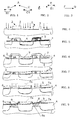
- Figures 1 to 3 show schematically various types of mutual placement of circuit elements,
- Figures 4 to 9 are respective schematic sectional views of a portion of an integrated circuit during the successive steps of a first embodiment of the method according to the invention,
- Figures 10 to 15 are respective schematic sectional views of a portion of an integrated circuit during successive steps of a second embodiment of the method according to the invention.
-
- A method for forming, on a semiconductor substrate, of structures self-aligned with each other is described here below with reference to the drawings.
- The method of the invention comprises a succession of processing steps. The steps described hereinafter are not a complete processing flow for the manufacturing of integrated circuits. This invention can be implemented in combination with current integrated circuit manufacturing techniques, and only those currently used steps, necessary for the understanding of the invention, will be described.
- The schematic drawings of portions of an integrated circuit undergoing manufacturing are not drawn to scale, but rather to illustrate major features of the invention.
- In particular, the method for forming self-aligned structures on a
semiconductor substrate 1, according to the invention, provides the formation, on thesemiconductor substrate 1, offirst regions semiconductor substrate 1. This first material may be an oxide layer. - A
protective layer semiconductor substrate 1. - Thereafter, the
protective layer first regions second regions protective layer substrate 1 and extended between thefirst regions - Two pluralities of
regions - By selectively removing the first plurality of
regions regions regions - Advantageously in this invention,
spacers regions - Thus, the width of the
regions protective layer 7 is varied to meet design requirements of the structures to be formed. - In one embodiment of the invention,
regions substrate 1 andspacers first regions - Once the
protective layer spacers regions - The distance between said
regions spacers - An embodiment of the method according to the invention, wherein two contiguous implanted areas, such as an extrinsic base region, intrinsic base region and emitter region of a bipolar transistor are formed, will now be described.
- A
first layer 2, e.g. an oxide layer, is deposited on asemiconductor substrate 1, e.g. a silicon substrate. Thefirst layer 2 is then patterned by using conventional lithographic and etching techniques for formingregions 3 projecting from thesemiconductor substrate 1. - Advantageously,
spacers 5 of a different material from that of thefirst layer 2, e.g. silicon nitride, are formed on the sidewalls of theregions 3 that have been used for masking the first implant. - A first implanting step is then carried out to form a first region or
junction 4, as shown in Figure 5. - The first implanted
region 4 is self-aligned with respect to theregions 3, and can be used for forming an extrinsic base region of a bipolar transistor. - Advantageously, a
metal layer 6, e.g. of a transition metal such as Titanium, Cobalt, or Nitride, is formed on thesubstrate 1. The whole device then undergoes a thermal treatment so that themetal layer 6, reacting withsubstrate 1 not covered with theregions 3 and thespacers 5, forms a silicide layer suitable for lowering the layer resistivity. - A
second layer 7, having selective etching properties with respect to thefirst layer 2, is then formed all over thesubstrate 1. - For example, the
second layer 7 is a silicon nitride layer deposited through CVD (Chemical Vapor Deposition), which results in theregions 5 that projecting from thesubstrate 1 being well covered. - According to the invention, the
layer 7 is then removed to expose thefirst layer 2 as shown in Figure 7. -
Regions 7a of thesecond layer 7 are thus bounded betweenregions 3 projecting from the substrate. - Advantageously, this removing step is a planarizing step carried out with a CMP technique, for example.
- At this stage, the
first regions 5 are etched away selectively, for instance by etching with a hydrofluoric acid solution. - By applying this selective etching, the
spacers 5 and regions of thesecond layer 7 left on thesubstrate 1 are not harmed. - A second implanting step is then carried out to form implanted
regions 8, 8a where, for example, respective emitter andbase junctions 8, 8a of a bipolar transistor may be formed. - This second implanting step is screened off in the areas in which the
first region 4 is there already by the secondprotective layer 7, as shown in Figure 9. - The
regions 7a oflayer 7 are then selectively etched away with respect to thesubstrate 1, by using warm hydrofluoric acid, for example. - Advantageously, these
regions 7a are used in subsequent processing steps, e.g. to complete the device and to establish self-aligned contact on the emitter, in case of a bipolar transistor. - Different material pairs may be used for forming the
regions 5 andprotective layer 7, provided that they can be deposited at low temperature and always planarized with the CMP technique, and be selectively removable one another and with respect to the substrate. - For example, the oxide and nitride layers could be exchanged, or a polycrystalline silicon deposited on a thin oxide layer could be used as
first layer 2, and an oxide ornitride layer 7 used assecond layer 7. - It can also be appreciated that the mutual placement of the first 4 and second junction 8 could be changed to suit the functional requirements of the device, by providing
spacers 5 of a suitable length and appropriate material before the first or the second implanting step is applied. - Advantageously,
second spacers 9 are formed on the sidewalls of thefirst spacers 5. Thesecond spacers 9 may be formed by means of a layer of Ti, Co, or Ni silicide. - The width of these
spacers 9 can be modulated by means of the amount of deposited material and the etching extent, thus obtaining a separation between thefirst spacers 5 that can easily reach sub-lithographic dimensions. - Shown in Figures 10 to 15 is a second embodiment of the inventive method.
- A first,
thin dielectric layer 10 and a first, thickprotective layer 11, e.g. 0.5 to 1 µm thick, are formed on asemiconductor substrate 1. Thefirst dielectric layer 10 may be an oxide layer whereas the second the firstprotective layer 11 may be a nitride layer, as shown in Figure 10. - The first
protective layer 11 is then patterned to form projecting regions orpillars 12, leaving thefirst dielectric layer 11 untouched as shown in Figure 11. - Advantageously, this patterning step is performed with a conventional technique and subsequent etching step through RIE (Reactive Ion Etching).
- Advantageously, spacers 14, made of a selective material with respect to the material of the
pillars 12, are formed on the sidewalls of thepillars 12 that have been used for masking the first implant. - A first, heavy implanting step is then carried out all over the
substrate 1 to form a first implantedregion 13. - The first implanted
region 13 is self-aligned with respect to thepillars 12, and may be used to form the extrinsic base region of a bipolar transistor. - Thermal treatments for activating the dopant to complete the first implanted
region 13 are then performed. - By providing the
spacers 14, potential problems of sideward diffusion are mitigated. - Advantageously, a
metal layer 15, e.g. of a transition metal such as Ti, Co, Ni, is deposited over the whole device. The whole device then undergoes a thermal treatment so that themetal layer 15, reacting with thesubstrate 1 not covered by thepillars 12, forms a silicide layer apt to reduce the layer resistivity. - According to the invention, a
protective layer 16 is deposited on thewhole substrate 1. Thisdielectric layer 16 may be a thick layer of pre-metal isolation oxide as shown in Figure 13. - This is followed by a planarizing step, e.g. through CMP, to expose the
pillars 12. -
Regions 16a of thesecond layer 16 are thus bounded between theregions 3 projecting from the substrate. - The
pillars 12 are then etched away selectively. Where thepillars 12 are made of silicon nitride, the selective etching may be performed either with warm hydrofluoric acid or a highly selective plasma. - The
layer 10 is then etched away from thesubstrate 1, by using a buffered solution, for example. - A second and a third implanting steps are then carried out to provide a second 17 and a third 17a implanted regions, the latter 17a being fully embedded in the
second region 17 as shown in Figure 15. - The second and third implanted
regions - The device is then completed through conventional processing steps. Particularly as far as bipolar transistors are concerned, the contact is formed conventionally.
- In this embodiment, the bipolar transistor base and emitter regions are self-aligned to the contact of the emitter region, with the etch prevented from harming the surface of the
substrate 1. Furthermore, the thermal treatments are avoided, these being associated with the formation of the extrinsic base region, which alter the profile of the emitter region. - Although the manufacturing method relates to the manufacturing of bipolar transistors, the method according to the invention can be used, for example, to obtain a polysilicon area self-aligned to an implant, , e.g. a deep anti-punch-through implant, which is not to end beneath the source-drain regions of a MOS transistor in order to reduce the junction capacitance.
- In summary, the method of the invention allows self-aligned structures to be defined, avoiding the cavities in the
substrate 1 and without involving any heavy thermal treatments. - In particular, the structures formed with this method are used as masks for the layer where they have been formed, or they are used themselves as active structures in an integrated circuit in which they are embedded.
- Where implanted regions are provided, the regions may be spaced apart as desired, even below lithography limits, in a controlled manner.
Claims (17)
- A method for forming structures self-aligned with each other on a semiconductor substrate (1), comprising the following steps:forming, on the semiconductor substrate (1), first regions (3,12) of a first material projecting from said semiconductor substrate (1);forming, on the whole of said semiconductor substrate (1), a protective layer (7,16) of a second material, said second material being selective with respect to said first material;removing said protective layer (7,16) to expose said first regions (3,12) through a planarizing step,;etching said first regions (3,12) to expose said semiconductor substrate (1), and forming second regions (7a,16a) projecting from the substrate (1) of said protective layer (7,16).
- A method for forming structures self-aligned with each other according to Claim 1, characterized in that it comprises the following steps:forming first spacers (5,14) of a second selective material with respect to the first material on the sidewalls of said first regions (3,12), before said protective layer (7,16) is formed.
- A method for forming structures self-aligned with each other according to Claim 2, characterized in that it comprises the following steps:etching said first regions (3,12) to expose said semiconductor substrate (1), and forming regions (7a,16a) projecting from the substrate of said protective layer.
- A method for forming structures self-aligned with each other according to Claim 1, characterized in that it comprises the following steps:carrying out an implanting step on the whole semiconductor substrate (1) to form, on said semiconductor substrate (1), first implanted regions (4,13) adjacent to said first regions (3,12), before the protective layer (7,16) is formed.
- A method for forming structures self-aligned with each other according to Claim 1, characterized in that it comprises the following steps:carrying out an implanting step on the whole of said semiconductor substrate (1) to form, on said semiconductor substrate (1), implanted regions (8,8a;17,17a) adjacent to said second regions (7a,16a).
- A method for forming structures self-aligned with each other according to Claim 2, characterized in that it comprises the following steps:forming second spacers (9) on the sidewalls of said first spacers (5).
- A method for forming structures self-aligned with each other according to Claim 2, characterized in that said first spacers (5,14) are made of a third material selective with respect to the first material.
- A method for forming structures self-aligned with each other according to Claim 6, characterized in that said second spacers (9) are made of a fourth material selective with respect to the first material.
- A method for forming structures self-aligned with each other according to Claim 1, characterized in that said planarizing step is carried out by using a CMP technique.
- A method for forming structures self-aligned with each other according to Claim 1, characterized in that said first material is a silicon oxide and said second material is silicon nitride.
- A method for forming structures self-aligned with each other according to Claim 1, characterized in that said first material is silicon nitride and said second material is a silicon oxide.
- A method for forming structures self-aligned with each other according to Claim 1, characterized in that it comprises the following steps:forming an additional protective layer (10) on the whole of said substrate (1) before forming said first regions (3,12) of a fifth material selective with respect to the first material.
- A method for forming structures self-aligned with each other according to Claim 8, characterized in that said third and fourth materials are silicon nitride.
- A method for forming structures self-aligned with each other according to Claim 8, characterized in that said fifth material is silicon oxide.
- A method for forming structures self-aligned with each other according to Claim 1, characterized in that said first implanted regions (4,13) are extrinsic base regions of a bipolar transistor, and that said at least second regions (8,8a;17,17a) are bipolar transistor emitter and base junctions (8,8a), respectively.
- A method for forming structures self-aligned with each other according to Claim 2, characterized in that it comprises the following steps:forming, on said semiconductor substrate (1), a metal layer (6,14) after said first spacers (5,14) are formed, and subsequent thermal treatment to selectively form a silicide layer on the substrate portions, that are exposed from said first regions (3,12), and said first spacers (5,14).
- A method for forming structures self-aligned with each other on a semiconductor substrate (1), comprising the following steps:etching said first spacers (5,14) to expose said semiconductor substrate (1), and forming regions (7a) projecting from the substrate of said protective layer.forming, on the semiconductor substrate (1), first regions (3,12) of a first material projecting from said semiconductor substrate (1);forming first spacers (5,14) of a second selective material with respect to the first material on the sidewalls of said first regions (3,12), before said protective layer (7,16) is formed;forming, over the whole of said semiconductor substrate (1), a protective layer (7,16) of a third material selective with respect to the second material;removing said protective layer to expose said first regions (3,12) through a planarizing step;
Priority Applications (2)
| Application Number | Priority Date | Filing Date | Title |
|---|---|---|---|
| EP02425806A EP1435647A1 (en) | 2002-12-30 | 2002-12-30 | Method for forming structures self-aligned with each other on a semiconductor substrate |
| US10/749,126 US20040188757A1 (en) | 2002-12-30 | 2003-12-30 | Method for forming structures self-aligned with each other on a semiconductor substrate |
Applications Claiming Priority (1)
| Application Number | Priority Date | Filing Date | Title |
|---|---|---|---|
| EP02425806A EP1435647A1 (en) | 2002-12-30 | 2002-12-30 | Method for forming structures self-aligned with each other on a semiconductor substrate |
Publications (1)
| Publication Number | Publication Date |
|---|---|
| EP1435647A1 true EP1435647A1 (en) | 2004-07-07 |
Family
ID=32479859
Family Applications (1)
| Application Number | Title | Priority Date | Filing Date |
|---|---|---|---|
| EP02425806A Withdrawn EP1435647A1 (en) | 2002-12-30 | 2002-12-30 | Method for forming structures self-aligned with each other on a semiconductor substrate |
Country Status (2)
| Country | Link |
|---|---|
| US (1) | US20040188757A1 (en) |
| EP (1) | EP1435647A1 (en) |
Cited By (1)
| Publication number | Priority date | Publication date | Assignee | Title |
|---|---|---|---|---|
| CN102637597A (en) * | 2011-02-10 | 2012-08-15 | 上海宏力半导体制造有限公司 | Vertical PNP (precision navigation processor) preparation method |
Citations (6)
| Publication number | Priority date | Publication date | Assignee | Title |
|---|---|---|---|---|
| US4927774A (en) * | 1988-06-10 | 1990-05-22 | British Telecommunications Plc | Self aligned bipolar fabrication process |
| US5132236A (en) * | 1991-07-30 | 1992-07-21 | Micron Technology, Inc. | Method of semiconductor manufacture using an inverse self-aligned mask |
| US5960270A (en) * | 1997-08-11 | 1999-09-28 | Motorola, Inc. | Method for forming an MOS transistor having a metallic gate electrode that is formed after the formation of self-aligned source and drain regions |
| US6225173B1 (en) * | 1998-11-06 | 2001-05-01 | Advanced Micro Devices, Inc. | Recessed channel structure for manufacturing shallow source/drain extensions |
| US20010039095A1 (en) * | 2000-01-21 | 2001-11-08 | Michel Marty | Process for producing a bipolar transistor with self-aligned emitter and extrinsic base |
| WO2002043132A1 (en) * | 2000-11-22 | 2002-05-30 | Conexant Systems, Inc. | Method for fabricating a self-aligned emitter in a bipolar transistor |
Family Cites Families (2)
| Publication number | Priority date | Publication date | Assignee | Title |
|---|---|---|---|---|
| US6200865B1 (en) * | 1998-12-04 | 2001-03-13 | Advanced Micro Devices, Inc. | Use of sacrificial dielectric structure to form semiconductor device with a self-aligned threshold adjust and overlying low-resistance gate |
| US6319807B1 (en) * | 2000-02-07 | 2001-11-20 | United Microelectronics Corp. | Method for forming a semiconductor device by using reverse-offset spacer process |
-
2002
- 2002-12-30 EP EP02425806A patent/EP1435647A1/en not_active Withdrawn
-
2003
- 2003-12-30 US US10/749,126 patent/US20040188757A1/en not_active Abandoned
Patent Citations (6)
| Publication number | Priority date | Publication date | Assignee | Title |
|---|---|---|---|---|
| US4927774A (en) * | 1988-06-10 | 1990-05-22 | British Telecommunications Plc | Self aligned bipolar fabrication process |
| US5132236A (en) * | 1991-07-30 | 1992-07-21 | Micron Technology, Inc. | Method of semiconductor manufacture using an inverse self-aligned mask |
| US5960270A (en) * | 1997-08-11 | 1999-09-28 | Motorola, Inc. | Method for forming an MOS transistor having a metallic gate electrode that is formed after the formation of self-aligned source and drain regions |
| US6225173B1 (en) * | 1998-11-06 | 2001-05-01 | Advanced Micro Devices, Inc. | Recessed channel structure for manufacturing shallow source/drain extensions |
| US20010039095A1 (en) * | 2000-01-21 | 2001-11-08 | Michel Marty | Process for producing a bipolar transistor with self-aligned emitter and extrinsic base |
| WO2002043132A1 (en) * | 2000-11-22 | 2002-05-30 | Conexant Systems, Inc. | Method for fabricating a self-aligned emitter in a bipolar transistor |
Cited By (1)
| Publication number | Priority date | Publication date | Assignee | Title |
|---|---|---|---|---|
| CN102637597A (en) * | 2011-02-10 | 2012-08-15 | 上海宏力半导体制造有限公司 | Vertical PNP (precision navigation processor) preparation method |
Also Published As
| Publication number | Publication date |
|---|---|
| US20040188757A1 (en) | 2004-09-30 |
Similar Documents
| Publication | Publication Date | Title |
|---|---|---|
| US7176137B2 (en) | Method for multiple spacer width control | |
| US7834406B2 (en) | High-voltage metal-oxide-semiconductor device and method of manufacturing the same | |
| US6218710B1 (en) | Method to ensure isolation between source-drain and gate electrode using self aligned silicidation | |
| US6673705B2 (en) | Method of manufacturing a MISFET having post oxide films having at least two kinds of thickness | |
| US6579764B2 (en) | Integrated circuit memory devices having non-volatile memory transistors and methods of fabricating the same | |
| JPH098303A (en) | Method for forming raised source / drain regions in an integrated circuit | |
| US6225175B1 (en) | Process for defining ultra-thin geometries | |
| US4075754A (en) | Self aligned gate for di-CMOS | |
| US6509264B1 (en) | Method to form self-aligned silicide with reduced sheet resistance | |
| CN111653484B (en) | A method to optimize the self-alignment process of silicon carbide MOSFETs | |
| US6372563B1 (en) | Self-aligned SOI device with body contact and NiSi2 gate | |
| US20250351544A1 (en) | Control of locos structure thickness without a mask | |
| KR100212455B1 (en) | Process for fabricating semiconductor device with dual gate structure | |
| US20040188757A1 (en) | Method for forming structures self-aligned with each other on a semiconductor substrate | |
| KR100240682B1 (en) | Manufacturing Method of Semiconductor Device | |
| US6977134B2 (en) | Manufacturing method of a MOSFET gate | |
| US6204129B1 (en) | Method for producing a high-voltage and low-voltage MOS transistor with salicide structure | |
| KR101130331B1 (en) | An advanced technique for forming transistors having raised drain and source regions with different height | |
| JP2001284557A (en) | Manufacturing method of nonvolatile semiconductor memory device | |
| KR100280527B1 (en) | MOS transistor manufacturing method | |
| US6362058B1 (en) | Method for controlling an implant profile in the channel of a transistor | |
| JP4065803B2 (en) | Manufacturing method of semiconductor device | |
| JP2002198437A (en) | Semiconductor device and method of manufacturing the same | |
| JPS6092666A (en) | Manufacture of mis transistor | |
| KR100361521B1 (en) | Method for manufacturing gate in semiconductor device |
Legal Events
| Date | Code | Title | Description |
|---|---|---|---|
| PUAI | Public reference made under article 153(3) epc to a published international application that has entered the european phase |
Free format text: ORIGINAL CODE: 0009012 |
|
| AK | Designated contracting states |
Kind code of ref document: A1 Designated state(s): AT BE BG CH CY CZ DE DK EE ES FI FR GB GR IE IT LI LU MC NL PT SE SI SK TR |
|
| AX | Request for extension of the european patent |
Extension state: AL LT LV MK RO |
|
| 17P | Request for examination filed |
Effective date: 20050103 |
|
| AKX | Designation fees paid |
Designated state(s): DE FR GB IT |
|
| STAA | Information on the status of an ep patent application or granted ep patent |
Free format text: STATUS: THE APPLICATION HAS BEEN WITHDRAWN |
|
| 17Q | First examination report despatched |
Effective date: 20050701 |
|
| 18W | Application withdrawn |
Effective date: 20050721 |