EP1434469A1 - Organic electroluminescence display and its driving method - Google Patents
Organic electroluminescence display and its driving method Download PDFInfo
- Publication number
- EP1434469A1 EP1434469A1 EP02741433A EP02741433A EP1434469A1 EP 1434469 A1 EP1434469 A1 EP 1434469A1 EP 02741433 A EP02741433 A EP 02741433A EP 02741433 A EP02741433 A EP 02741433A EP 1434469 A1 EP1434469 A1 EP 1434469A1
- Authority
- EP
- European Patent Office
- Prior art keywords
- organic
- voltage
- display device
- organic electroluminescence
- electroluminescence display
- Prior art date
- Legal status (The legal status is an assumption and is not a legal conclusion. Google has not performed a legal analysis and makes no representation as to the accuracy of the status listed.)
- Withdrawn
Links
Images


Classifications
-
- G—PHYSICS
- G09—EDUCATION; CRYPTOGRAPHY; DISPLAY; ADVERTISING; SEALS
- G09G—ARRANGEMENTS OR CIRCUITS FOR CONTROL OF INDICATING DEVICES USING STATIC MEANS TO PRESENT VARIABLE INFORMATION
- G09G3/00—Control arrangements or circuits, of interest only in connection with visual indicators other than cathode-ray tubes
- G09G3/20—Control arrangements or circuits, of interest only in connection with visual indicators other than cathode-ray tubes for presentation of an assembly of a number of characters, e.g. a page, by composing the assembly by combination of individual elements arranged in a matrix no fixed position being assigned to or needed to be assigned to the individual characters or partial characters
- G09G3/22—Control arrangements or circuits, of interest only in connection with visual indicators other than cathode-ray tubes for presentation of an assembly of a number of characters, e.g. a page, by composing the assembly by combination of individual elements arranged in a matrix no fixed position being assigned to or needed to be assigned to the individual characters or partial characters using controlled light sources
- G09G3/30—Control arrangements or circuits, of interest only in connection with visual indicators other than cathode-ray tubes for presentation of an assembly of a number of characters, e.g. a page, by composing the assembly by combination of individual elements arranged in a matrix no fixed position being assigned to or needed to be assigned to the individual characters or partial characters using controlled light sources using electroluminescent panels
-
- G—PHYSICS
- G09—EDUCATION; CRYPTOGRAPHY; DISPLAY; ADVERTISING; SEALS
- G09G—ARRANGEMENTS OR CIRCUITS FOR CONTROL OF INDICATING DEVICES USING STATIC MEANS TO PRESENT VARIABLE INFORMATION
- G09G3/00—Control arrangements or circuits, of interest only in connection with visual indicators other than cathode-ray tubes
- G09G3/20—Control arrangements or circuits, of interest only in connection with visual indicators other than cathode-ray tubes for presentation of an assembly of a number of characters, e.g. a page, by composing the assembly by combination of individual elements arranged in a matrix no fixed position being assigned to or needed to be assigned to the individual characters or partial characters
- G09G3/2007—Display of intermediate tones
- G09G3/2014—Display of intermediate tones by modulation of the duration of a single pulse during which the logic level remains constant
-
- G—PHYSICS
- G09—EDUCATION; CRYPTOGRAPHY; DISPLAY; ADVERTISING; SEALS
- G09G—ARRANGEMENTS OR CIRCUITS FOR CONTROL OF INDICATING DEVICES USING STATIC MEANS TO PRESENT VARIABLE INFORMATION
- G09G3/00—Control arrangements or circuits, of interest only in connection with visual indicators other than cathode-ray tubes
- G09G3/20—Control arrangements or circuits, of interest only in connection with visual indicators other than cathode-ray tubes for presentation of an assembly of a number of characters, e.g. a page, by composing the assembly by combination of individual elements arranged in a matrix no fixed position being assigned to or needed to be assigned to the individual characters or partial characters
- G09G3/22—Control arrangements or circuits, of interest only in connection with visual indicators other than cathode-ray tubes for presentation of an assembly of a number of characters, e.g. a page, by composing the assembly by combination of individual elements arranged in a matrix no fixed position being assigned to or needed to be assigned to the individual characters or partial characters using controlled light sources
- G09G3/30—Control arrangements or circuits, of interest only in connection with visual indicators other than cathode-ray tubes for presentation of an assembly of a number of characters, e.g. a page, by composing the assembly by combination of individual elements arranged in a matrix no fixed position being assigned to or needed to be assigned to the individual characters or partial characters using controlled light sources using electroluminescent panels
- G09G3/32—Control arrangements or circuits, of interest only in connection with visual indicators other than cathode-ray tubes for presentation of an assembly of a number of characters, e.g. a page, by composing the assembly by combination of individual elements arranged in a matrix no fixed position being assigned to or needed to be assigned to the individual characters or partial characters using controlled light sources using electroluminescent panels semiconductive, e.g. using light-emitting diodes [LED]
- G09G3/3208—Control arrangements or circuits, of interest only in connection with visual indicators other than cathode-ray tubes for presentation of an assembly of a number of characters, e.g. a page, by composing the assembly by combination of individual elements arranged in a matrix no fixed position being assigned to or needed to be assigned to the individual characters or partial characters using controlled light sources using electroluminescent panels semiconductive, e.g. using light-emitting diodes [LED] organic, e.g. using organic light-emitting diodes [OLED]
- G09G3/3225—Control arrangements or circuits, of interest only in connection with visual indicators other than cathode-ray tubes for presentation of an assembly of a number of characters, e.g. a page, by composing the assembly by combination of individual elements arranged in a matrix no fixed position being assigned to or needed to be assigned to the individual characters or partial characters using controlled light sources using electroluminescent panels semiconductive, e.g. using light-emitting diodes [LED] organic, e.g. using organic light-emitting diodes [OLED] using an active matrix
- G09G3/3258—Control arrangements or circuits, of interest only in connection with visual indicators other than cathode-ray tubes for presentation of an assembly of a number of characters, e.g. a page, by composing the assembly by combination of individual elements arranged in a matrix no fixed position being assigned to or needed to be assigned to the individual characters or partial characters using controlled light sources using electroluminescent panels semiconductive, e.g. using light-emitting diodes [LED] organic, e.g. using organic light-emitting diodes [OLED] using an active matrix with pixel circuitry controlling the voltage across the light-emitting element
-
- H—ELECTRICITY
- H05—ELECTRIC TECHNIQUES NOT OTHERWISE PROVIDED FOR
- H05B—ELECTRIC HEATING; ELECTRIC LIGHT SOURCES NOT OTHERWISE PROVIDED FOR; CIRCUIT ARRANGEMENTS FOR ELECTRIC LIGHT SOURCES, IN GENERAL
- H05B45/00—Circuit arrangements for operating light-emitting diodes [LED]
- H05B45/60—Circuit arrangements for operating LEDs comprising organic material, e.g. for operating organic light-emitting diodes [OLED] or polymer light-emitting diodes [PLED]
-
- H—ELECTRICITY
- H10—SEMICONDUCTOR DEVICES; ELECTRIC SOLID-STATE DEVICES NOT OTHERWISE PROVIDED FOR
- H10K—ORGANIC ELECTRIC SOLID-STATE DEVICES
- H10K50/00—Organic light-emitting devices
- H10K50/80—Constructional details
-
- H—ELECTRICITY
- H10—SEMICONDUCTOR DEVICES; ELECTRIC SOLID-STATE DEVICES NOT OTHERWISE PROVIDED FOR
- H10K—ORGANIC ELECTRIC SOLID-STATE DEVICES
- H10K59/00—Integrated devices, or assemblies of multiple devices, comprising at least one organic light-emitting element covered by group H10K50/00
- H10K59/10—OLED displays
- H10K59/12—Active-matrix OLED [AMOLED] displays
-
- H—ELECTRICITY
- H10—SEMICONDUCTOR DEVICES; ELECTRIC SOLID-STATE DEVICES NOT OTHERWISE PROVIDED FOR
- H10K—ORGANIC ELECTRIC SOLID-STATE DEVICES
- H10K85/00—Organic materials used in the body or electrodes of devices covered by this subclass
- H10K85/30—Coordination compounds
- H10K85/341—Transition metal complexes, e.g. Ru(II)polypyridine complexes
- H10K85/342—Transition metal complexes, e.g. Ru(II)polypyridine complexes comprising iridium
-
- G—PHYSICS
- G09—EDUCATION; CRYPTOGRAPHY; DISPLAY; ADVERTISING; SEALS
- G09G—ARRANGEMENTS OR CIRCUITS FOR CONTROL OF INDICATING DEVICES USING STATIC MEANS TO PRESENT VARIABLE INFORMATION
- G09G2300/00—Aspects of the constitution of display devices
- G09G2300/08—Active matrix structure, i.e. with use of active elements, inclusive of non-linear two terminal elements, in the pixels together with light emitting or modulating elements
- G09G2300/0809—Several active elements per pixel in active matrix panels
- G09G2300/0842—Several active elements per pixel in active matrix panels forming a memory circuit, e.g. a dynamic memory with one capacitor
-
- G—PHYSICS
- G09—EDUCATION; CRYPTOGRAPHY; DISPLAY; ADVERTISING; SEALS
- G09G—ARRANGEMENTS OR CIRCUITS FOR CONTROL OF INDICATING DEVICES USING STATIC MEANS TO PRESENT VARIABLE INFORMATION
- G09G2310/00—Command of the display device
- G09G2310/02—Addressing, scanning or driving the display screen or processing steps related thereto
- G09G2310/0243—Details of the generation of driving signals
- G09G2310/0251—Precharge or discharge of pixel before applying new pixel voltage
-
- G—PHYSICS
- G09—EDUCATION; CRYPTOGRAPHY; DISPLAY; ADVERTISING; SEALS
- G09G—ARRANGEMENTS OR CIRCUITS FOR CONTROL OF INDICATING DEVICES USING STATIC MEANS TO PRESENT VARIABLE INFORMATION
- G09G2310/00—Command of the display device
- G09G2310/02—Addressing, scanning or driving the display screen or processing steps related thereto
- G09G2310/0243—Details of the generation of driving signals
- G09G2310/0254—Control of polarity reversal in general, other than for liquid crystal displays
- G09G2310/0256—Control of polarity reversal in general, other than for liquid crystal displays with the purpose of reversing the voltage across a light emitting or modulating element within a pixel
-
- G—PHYSICS
- G09—EDUCATION; CRYPTOGRAPHY; DISPLAY; ADVERTISING; SEALS
- G09G—ARRANGEMENTS OR CIRCUITS FOR CONTROL OF INDICATING DEVICES USING STATIC MEANS TO PRESENT VARIABLE INFORMATION
- G09G2310/00—Command of the display device
- G09G2310/06—Details of flat display driving waveforms
- G09G2310/066—Waveforms comprising a gently increasing or decreasing portion, e.g. ramp
-
- G—PHYSICS
- G09—EDUCATION; CRYPTOGRAPHY; DISPLAY; ADVERTISING; SEALS
- G09G—ARRANGEMENTS OR CIRCUITS FOR CONTROL OF INDICATING DEVICES USING STATIC MEANS TO PRESENT VARIABLE INFORMATION
- G09G2320/00—Control of display operating conditions
- G09G2320/02—Improving the quality of display appearance
- G09G2320/0247—Flicker reduction other than flicker reduction circuits used for single beam cathode-ray tubes
-
- G—PHYSICS
- G09—EDUCATION; CRYPTOGRAPHY; DISPLAY; ADVERTISING; SEALS
- G09G—ARRANGEMENTS OR CIRCUITS FOR CONTROL OF INDICATING DEVICES USING STATIC MEANS TO PRESENT VARIABLE INFORMATION
- G09G2320/00—Control of display operating conditions
- G09G2320/04—Maintaining the quality of display appearance
- G09G2320/043—Preventing or counteracting the effects of ageing
-
- Y—GENERAL TAGGING OF NEW TECHNOLOGICAL DEVELOPMENTS; GENERAL TAGGING OF CROSS-SECTIONAL TECHNOLOGIES SPANNING OVER SEVERAL SECTIONS OF THE IPC; TECHNICAL SUBJECTS COVERED BY FORMER USPC CROSS-REFERENCE ART COLLECTIONS [XRACs] AND DIGESTS
- Y02—TECHNOLOGIES OR APPLICATIONS FOR MITIGATION OR ADAPTATION AGAINST CLIMATE CHANGE
- Y02B—CLIMATE CHANGE MITIGATION TECHNOLOGIES RELATED TO BUILDINGS, e.g. HOUSING, HOUSE APPLIANCES OR RELATED END-USER APPLICATIONS
- Y02B20/00—Energy efficient lighting technologies, e.g. halogen lamps or gas discharge lamps
- Y02B20/30—Semiconductor lamps, e.g. solid state lamps [SSL] light emitting diodes [LED] or organic LED [OLED]
Definitions
- This invention relates to an organic electroluminescence display device (which may be referred to as an organic EL display device hereinafter), and a method for driving the same. More specifically, the invention relates to an organic EL display device which consumes a low electric power and is capable of obtaining a long luminous life span, and a method for driving the same.
- an active driving type organic EL luminous device having a thin film transistor, (which may be referred to as a TFT hereinafter), so as to drive organic EL elements.
- Such active driving type organic EL luminous devices have characteristics that the driving voltage thereof is largely lowered, the luminescence efficiency is improved and further the consumption power can be reduced with compared to simple driving type organic EL luminous devices.
- an active driving type organic EL luminous device having such advantageous effects has a compound having the light emitting property to which the triplet state contributes (hereinafter referred to as triplet-related compound), for example, an organic luminescent medium containing an iridium complex, a high luminescence brightness is obtained whereas a problem that the luminous life span is short is encountered. That is, in triplet-related compounds, the time when the molecules thereof are excited and relaxed is longer in the case of compounds having the light property related to the singlet state. Hence, electric charge is stored inside, so that the balance between holes and electrons is liable to be destroyed. Thus, according to Japan Journal of Applied Physics, Vol. 38, pp.
- the luminescence efficiency thereof is a value of 40 lumens/W or more under the condition that the luminescence brightness is 500 cd/cm 2 but the half life thereof is a short time of 200 hours or less.
- an organic EL display device which consumes a low electric power and is drivable for a long time can be provided by driving the device through an appropriately-set driving circuit even if a combination of a host compound with a triplet-related luminous compound is used; accordingly, the display device can be applied to the field of flat panel displays and others.
- an object of the present invention is to provide an organic EL display device which consumes a low electric power and gives a less drop in luminescence brightness even when the device is driven for a long time.
- Another object of the present invention is to provide a driving method capable of driving such an organic EL display device at a low consumption power for a long time.
- an organic EL display device comprising an organic EL element having a structure wherein an organic luminescent medium comprising a host compound and a phosphorescent luminous compound is sandwiched between a top electrode and a bottom electrode; and a driving circuit for applying a electric pulse current or pulse voltage having a frequency of 30 Hz or more and a duty ratio of 1/5 or less so as to drive the organic EL element.
- the organic EL display device having such a structure makes it possible to make consumption power low even if a triplet-related luminous compound is used, and further to make the luminous life span thereof long.
- the present invention has a driving circuit for applying the electric pulse voltage or pulse current to cause the organic luminescent medium to emit luminescence, and subsequently applying a voltage (V2) in the direction reverse to' that of the voltage (V1) of the pulse wave applied between the electrodes of the organic electroluminescence element.
- the organic EL display device having such a structure makes it possible to make the luminous life span longer since electric charge stored inside can be removed even when a triplet-related luminous compound is used as the organic luminescent medium.
- the organic EL display device of the present invention has a driving circuit for applying the voltage (V2) which is a smaller than the voltage (V1) of the pulse wave and is in the direction reverse to that of the voltage (V1).
- the organic EL display device having such a structure makes it possible to make the luminous life span still longer even when a triplet-related luminous compound is used.
- the triplet-related luminous compound is an organic metal complex.
- the organic EL display device having such a structure makes it possible to make consumption power lower.
- the organic metal complex comprises at least one metal selected from the group consisting of Ir, Pt, Pd, Ru, Rh, Mo, Re, Pb and Bi.
- the organic EL display device having such a structure makes it possible to make consumption power lower.
- the organic EL display device of the present invention comprises a hole barrier layer between the organic luminescent medium and the cathode.
- the organic EL display device having such a structure makes it possible to make consumption power lower even if a triplet-related luminous compound is used, and further to make the luminous life span longer.
- the hole barrier layer comprises a phenanthroline derivative.
- the organic EL display device having such a structure makes it possible to make consumption power lower even if a triplet-related luminous compound is used, and further to make the luminous life span longer.
- the driving circuit comprises a thin film transistor for controlling the luminescence of the organic EL element.
- the organic EL display device having such a structure makes it possible to make consumption power lower even if a triplet-related luminous compound is used, and further to make the luminous life span longer.
- Another aspect of the present invention is a method for driving an organic luminescence display device comprising an organic electroluminescence element having a structure wherein an organic luminescent medium is sandwiched between a top electrode and a bottom electrode, comprising applying a electric pulse current or pulse voltage having a frequency of 30 Hz or more and a duty ratio of 1/5 or less by means of a driving circuit, so as to drive the organic electroluminescence element.
- the electric pulse current is applied.
- the driving circuit applies the electric pulse voltage or pulse current to cause the organic luminescent medium to emit luminescence, and subsequently applies a voltage (V2) in the direction reverse to that of the voltage (V1) of the pulse wave applied between the electrodes of the organic electroluminescence element.
- the organic EL display device By driving the organic EL display device in this way, the luminous life span can be made longer since electric charges stored inside can be effectively removed even when a triplet-related luminous compound is used.
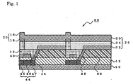
- an organic EL luminous device of a first embodiment is an organic EL display device 30 having an organic EL element 26 wherein an organic luminescent medium 24 is sandwiched between a top electrode 20 and a bottom electrode 22, which are set over a supporting substrate 10, and a driving circuit 14 for driving the organic EL element 26, wherein the organic luminescent medium 24 comprises a host compound and a triplet-related luminous compound, and further the driving circuit 14 can apply an electric pulse voltage (V1) or pulse current having a frequency of 30 Hz or more and a duty ratio of 1/5 or less, the voltage (V1) being applied between the electrodes of the organic EL element 26 at this time.
- V1 electric pulse voltage
- a TFT circuit is set up. However, this TFT circuit may be omitted.
- Organic EL display devices wherein a TFT circuit is set up are usually driven by direct current whereas the above-mentioned electric pulse voltage or pulse current is applied in the present invention.
- the support substrate in the organic EL display device (which may be referred to as the substrate hereinafter), is a member for supporting the organic EL element, the driving circuit, and others. It is therefore preferable that the substrate is excellent in mechanical strength and dimension stability.
- Such a substrate include a glass plate, a metal plate, a ceramic plate or a plastic plate (such as polycarbonate resin, acrylic resin, vinyl chloride resin, polyethylene terephthalate resin, polyimide resin, polyester resin, epoxy resin, phenol resin, silicon resin or fluorine-containing resin).
- a plastic plate such as polycarbonate resin, acrylic resin, vinyl chloride resin, polyethylene terephthalate resin, polyimide resin, polyester resin, epoxy resin, phenol resin, silicon resin or fluorine-containing resin.
- the substrate made of these materials In order to avoid the invasion of moisture into the organic EL display device, it is preferable to subject the substrate made of these materials to moisture proof treatment or hydrophobic treatment by forming an inorganic film further or applying a fluorine-containing resin.
- the water content in the substrate and the gas permeability coefficient thereof small by moisture proofing treatment or hydrophobic treatment. Specifically, it is preferable to set the water content in the supporting substrate and the gas permeability coefficient into 0.0001% by weight or less and 1 ⁇ 10 -13 or less cc ⁇ cm/cm 2 ⁇ sec.cmHg, respectively.
- the organic luminescent medium can be defined as a medium containing an organic emitting layer wherein an electron and a hole are recombined with each other so that EL luminescence can be emitted.
- This organic luminescent medium can be constructed, for example, by laminating the following respective layers on the bottom electrode.
- the triplet-related luminous compound may be contained in any of the following organic layers.
- Examples of the luminous material (host compound) in the organic luminescent medium include only one or combinations of two or more selected from carbazole derivatives, p-quaterphenyl derivatives, p-quinquephenyl derivatives, benzothiazole compounds, benzimidazole compounds, benzoxazole compounds, metal-chelated oxynoid compounds, oxadiazole compounds, styrylbenzene compounds, distyrylpyrazine derivatives, butadiene compounds, naphthalimide compounds, perylene derivatives, aldazine derivatives, pyraziline derivatives, cyclopentadiene derivatives, pyrrolopyrrole derivatives, styrylamine derivatives, coumarin compounds, aromatic dimethylidyne compounds, metal complexes each having an 8-quinolinol derivative as a ligand, and polyphenyl compounds.
- DTBPBBi 4,4'-bis(2,2-di-t-butylphenylvinyl)biphenyl
- DPVBi 4,4'-bis(2,2-diphenylvinyl)biphenyl
- the host compound is preferably a compound having a larger singlet excitation energy than the level of the triplet excitation energy obtained by the triplet-related luminous compound so that the host compound can use the triplet excitation energy, and is more preferably a compound having a larger triplet excitation energy than the energy level.
- the phosphorescent luminous compound is a compound which generates phosphorescence. It is sufficient that the phosphorescent luminous compound is a compound which has an excitation state life span of 100 ns or more, and its life span can be measured as a luminescence relaxation component. As the method of measuring the life span, the time dependent measurement of transit luminescent delay can be used.
- Lx ligand examples include acetylacetone derivatives (acac) and picoline derivatives (pic).
- Examples of such a triplet-related luminous compound include only one or combinations of two or more selected from an iridium complex, a platinum complex, a palladium complex, a ruthenium complex, a rubidium complex, a molybdenum complex, and a rhenium complex.
- triplet-related luminous compounds more specifically, the following are more preferable: tris(2-phenylpyridyl)iridium (abbreviated to Ir(ppy) 3 ), bis(2-phenylpyridyl)platinum, tris(2-phenylpyridyl)palladium, tris(2-phenylpyridyl)ruthenium, tris(2-phenylpyridyl)rubidium, tris(2-phenylpyridyl)molybdenum, Ir(ppy) 2 (acac), Ir(btp) 2 (acac), BtpPt(acac), Ir(bo) 2 (acac), Ir(bt) 2 (acac), Ir(ppy) 2 (Pic), and Ir(btp) 2 (pic).
- triplet-related luminous compounds can give luminescence property related to the triplet state even at room temperature.
- These complexes may have a substituent.
- substituents include alkyl groups, fluorine, and aryl groups.
- the ionization potential of the triplet-related luminous compound is larger than the ionization potential of the host compound.
- the amount of-the added triplet-related luminous compound is preferably set into 0.1 to 50% by weight of the total amount of the organic luminescent medium.
- the amount of the added triplet-related luminous compound is more preferably set into 1 to 30% by weight of the total amount of the organic luminescent medium, and still more preferably set into 5 to 20% by weight thereof.
- a bis(diarylamino)arylene derivative wherein the aryl is a polyphenyl and the arylene is a polyphenylene since the life span thereof is particularly long.
- the polyphenyl is preferably biphenyl or terphenyl, and the polyphenylene is preferably biphenylyl or terphenylyl.
- Examples of electron injection material which constitutes the electron injection layer include only one or combinations of two or more selected from tris (8-quinolinolate) aluminum, tris(8-quinolinolate) gallium, bis(10-benz[h]quinolinolate) beryllium, triazole derivatives, oxadiazole derivatives, triazine derivatives, perylene derivatives, quinoline derivatives, quinoxaline derivatives, diphenylquinone derivatives, nitro-substituted fluorenone derivatives, thiopyrandioxide derivatives.
- the thickness of the organic luminescent medium is not particularly limited.
- the thickness is preferably set into 5 nm to 5 ⁇ m.
- the thickness of the organic luminescent medium is less than 5 nm, the luminescence brightness or durability may lower; whereas if the thickness of the organic luminescent medium is more than 5 ⁇ m, the value of applying-voltage may become high.
- the thickness of the organic luminescent medium is more preferably set into 10 nm to 3 ⁇ m, and still more preferably set into 20 nm to 1 ⁇ m.
- the top electrode and the bottom electrode are described hereinafter.
- the top electrode and the bottom electrode correspond to an anode layer and a cathode layer, respectively, and a cathode layer and an anode layer, respectively, correspondingly to the structure of the organic EL element.
- the bottom electrode corresponds to an anode layer or a cathode layer, correspondingly to the structure of the EL display device.
- a metal, alloy or electrically conductive compound which has a large work function (for example, 4.0 eV or more), or a mixture thereof.
- an electrode material such as indium tin oxide, indium zinc oxide, strontium copper oxide, tin oxide, zinc oxide, gold, platinum or palladium, alone, or use a combination of two or more of these electrode materials.
- the bottom electrode which has a uniform thickness can be formed by a method capable of forming a film in a dry state, such as vapor deposition, sputtering, ion plating, electron beam vapor deposition, CVD (chemical vapor deposition), MOCVD (metal oxide chemical vapor deposition), or plasma CVD (plasma enhanced chemical vapor deposition).
- a method capable of forming a film in a dry state such as vapor deposition, sputtering, ion plating, electron beam vapor deposition, CVD (chemical vapor deposition), MOCVD (metal oxide chemical vapor deposition), or plasma CVD (plasma enhanced chemical vapor deposition).
- EL luminescence has to be taken out from the side of the bottom electrode in the present invention, it is necessary to make the bottom electrode to be a transparent electrode. It is therefore preferable to use the above-mentioned electrode material to set the transmittance of EL luminescence into 70% or more.
- the film thickness of the bottom electrode is not particularly limited.
- the thickness is preferably set into 10 to 1,000 nm, and more preferably set into 10 to 200 nm.
- the top electrode also corresponds to an anode layer or a cathode layer, correspondingly to the structure of the EL display device.
- a metal, alloy or electrically conductive compound which has a smaller work function (for example, less than 4.0 eV) than the anode layer, or a mixture or inclusion thereof.
- an electrode material such as sodium, sodium-potassium alloy, cesium, magnesium, lithium, magnesium-silver alloy, aluminum, aluminum oxide, aluminum-lithium alloy, indium, a rare earth metal, a mixture of these metals and an organic luminescent medium material, or a mixture of these metals and an electron injection layer material, alone, or use a combination of two or more of these electrode materials.
- the film thickness of the top electrode is not particularly limited, either. Specifically, the thickness is preferably set into 10 to 1,000 nm, and more preferably set into 10 to 200 nm.
- the top electrode 20 is preferably composed of a main electrode 16, and an auxiliary electrode 18 made of the material with a lower resistivity.
- Such a structure makes it possible to make the sheet resistance of the top electrode 20 remarkably low. Hence, the density of electric current flowing through the organic luminescent medium can be reduced. As a result, the life span of the organic luminescent medium can be made remarkably long.
- a color converting medium on the luminous surface of the organic EL element.
- a color converting medium include a color filter, and a fluorescent film for emitting light in color different from that of EL luminescence. A combination thereof is also preferable.
- the color filter is set up to decompose or filter light, thereby adjusting color or improving contrast, and is made as a dye layer made of only a dye, or as a lamellar matter made by dissolving or dispersing a dye into a binder resin.
- the color filter it is preferable to contain dyes in blue, green and red. This is because a combination of such a color filter with an organic EL element which emits white luminescence makes it possible to obtain the three primary colors of light, blue, green and red, and display full color.
- the fluorescent mediums in the organic EL display device have a function of absorbing luminescence of the organic EL element to emit fluorescence having a longer wavelength, and are made as a layer which are separately arranged in a planar direction. Respective fluorescent medium pieces are preferably arranged to correspond to luminous areas of the organic EL element, for example, positions of cross portions of the bottom electrode and the top electrode. Such a structure makes it possible that when the organic emitting layer in the cross portions of the bottom electrode and the top electrode emits luminescence, the respective fluorescent medium pieces receive the light and then luminescence in different colors (wavelengths) can be taken out.
- a light shielding layer black matrix for blocking luminescence of the organic EL element and light from the respective fluorescent medium pieces to improve contrast and decrease the dependency on field angle.
- the fluorescent medium may be constructed to be combined with the above-mentioned color filter.
- this voltage value is less than 1 V, a desired luminescence brightness is not obtained; whereas if this voltage value is more than 20 V, consumption power may be large.
- the voltage value when voltage is applied or electric current is injected is preferably set into 3 to 15 V, and still more preferably set into 8 to 13 V.
- the frequency when voltage is applied or electric current is injected is preferably set into 40 to 120 Hz, and more preferably set into 50 to 100 Hz.
- the duty ratio when voltage is applied or electric current is injected is preferably set into 1/1000 to 1/10, and more preferably set into 1/500 to 1/20.
- the half life tends to be shorter as the duty ratio is larger.
- the duty ratio changes largely within a range that the duty ratio is from 0.1 to 0.2.
- the half life which is about 400 Hrs in the case that the duty ratio is 0.1, exceeds 0.2, the half life falls to about 200 Hrs.
- this duty ratio is set into a value of 1/5 or less, that is, a value of 0.2 or less, a relatively long half life can be obtained. If this duty ratio is set into a value of 0.1 or less, a longer half life can be obtained but the value of the half life tends to be saturated.
- the duty ratio indispensably set into 1/5 or less, preferably set into 1/1000 to 1/10, and more preferably set into 1/500 to 1/20, as described above. This result is a reason for daring to adopt the above-mentioned duty ratio in active driving, which is originally DC-driven.
- TFT Thin film transistor
- the organic EL display device of the present invention preferably has at least one TFT 14 and an organic EL element 26 driven by this TFT 14 on or over a supporting substrate 10.
- an interlayer insulating film 13 and a color converting medium 60 which are made flat, are arranged between the TFT 14 and a bottom electrode 22 of the organic EL element 26, and a drain 47 of the TFT 14 is electrically connected to the bottom electrode 22 of the organic EL element 26 through an electrically connecting member 28 placed in the boundary between the interlayer insulating film 13 and the color converting medium 60.
- a circuit diagram of Fig. 3 including a TFT and a layout plan of Fig. 4 including the TFT to the TFT 14 are electrically connected plural scan electrode lines (Yj to Yj+n) 50, (the number of which is n, and n is, for example, from 1 to 1,000), and signal electrode lines (Xi to Xi+n) 51, which are arranged in an XY matrix form. Furthermore, common electrode lines (Ci to Ci+n) 52 laid in parallel to the signal electrode lines 51 are electrically connected to the TFT 14.
- these electrode lines 50, 51 and 52 are electrically connected to the TFT 14 and they are combined with condensers 57 to constitute electric switches for driving the organic EL elements 26.
- the electric switches are electrically connected to the scan electrode lines 50, the signal electrode lines 51 and others, and are further composed of, for example, one or more first transistors (which may be referred to as Tr1 hereinafter) 55, second transistors (which may be referred to as Tr2 hereinafter) 56, and condensers 57.
- the first transistor 55 has a function of selecting a luminous pixel and the second transistor 56 has a function of driving an organic EL element.
- an active layer 44 of the first transistor (Tr1) 55 and the second transistor (Tr2) 56 is composed of semiconductor areas 45 and 47 doped into n type and a non-doped semiconductor area 46, and can be represented by n+/i/n+.
- the semiconductor areas doped into the n type become a source 45 and the drain 47, respectively, and they are combined with a gate 43 provided to the upper of the non-doped semiconductor area across a gate oxide film 12 so as to constitute the transistors 55 and 56 as a whole.
- the semiconductor areas 45 and 47 which are doped into the n type, may be doped into p type to make a structure of p+/i/p+.
- the active layer 44 of the first transistor (Tr1) 55 and the second transistor (Tr2) 56 is preferably made of an inorganic semiconductor such as polysilicon, or an organic semiconductor such as thiophene oligomer or poly (p-phenylenevinylene). Polysilicon is a particularly preferable material since it is more stable against electric conduction than amorphous Si( ⁇ -Si).
- this TFT includes the first transistor (Tr1) 55 and the second transistor (Tr2) 56 and further constitutes an electric switch, as illustrated in Fig. 3.
- the electric switch having such a structure makes it possible to input a scan signal pulse and a signal pulse through electrodes in an XY matrix form and perform switching operation, thereby driving the organic EL element 26.
- the organic EL element 26 is caused to emit light or the light emission is stopped, whereby an image can be displayed.
- a desired one of the first transistors (Tr1) 55 is selected by a scan pulse transmitted through the scan electrode, lines (which may be referred to as gate lines) (Yj to Yj+n) 50 and a scan pulse transmitted through the signal electrode lines (Xi to Xi+n) 51, so that a given electric charge is collected in one of the condensers 57 formed between the common electrode lines (Ci to Ci+n) 52 and the source 45 of the first transistor (Tr1) 55.
- the gate voltage of the second transistor (Tr2) 56 turns to a constant value, so that the second transistor (Tr2) 56 turns into an ON-state. In this ON-state, the gate voltage is held until a next gate pulse is transmitted. Accordingly, electric current continues to be supplied to the bottom electrode 22 of the organic EL element 26 connected to the drain 47 of the second transistor (Tr2) 56.
- the organic EL element 26 can be driven by the supplied electric current.
- the driving voltage of the organic EL element 26 can be largely lowered and the luminescence efficiency can be improved.
- the consumption power can be reduced.
- a sealing part it is preferable to provide a sealing part to the organic EL display device. It is preferable to set such a sealing part onto the surrounding of the organic EL display device in order to prevent the invasion of moisture therein, or to insert a known sealing medium, such as a drying agent, a dry gas, or an inert gas such as fluorohydrocarbon, air-tightly between the sealing part set in this way and the organic EL display device.
- a known sealing medium such as a drying agent, a dry gas, or an inert gas such as fluorohydrocarbon
- This sealing part can be used as a supporting substrate in the case that the fluorescent or the color filter is set outside the top electrode.
- the same material as constitutes the supporting substrate for example, a glass plate can be used.
- a thin film layer made of oxide, oxynitride, nitride, sulfide or the like may also be used.
- Preferred examples of this material include SiO x (1 ⁇ x ⁇ 2), SiO x N y (1 ⁇ x ⁇ 2, and 0 ⁇ y ⁇ 1.5), AlO x (0.6 ⁇ x ⁇ 1.5), AlON, SiAlON, SiC, and SiCN.
- x or y represents a composition ratio, and SiAlON or the like, in which neither x nor y is indicated, represents any composition ratio).
- the form of the sealing part is not particularly limited.
- the form is preferably made up, for example, to a plate form or a cap form.
- the thickness thereof is preferably set into 0.01 to 5 mm.
- a second embodiment is an organic EL display device comprising an organic EL element having a structure wherein an organic luminescent medium is sandwiched between a top electrode and a bottom electrode, and a driving circuit for driving the organic EL element, wherein the organic luminescent medium comprises a host compound and a triplet-related luminous compound; the driving circuit applies a electric pulse voltage or pulse current having a frequency of 30 Hz or more and a duty ratio of 1/5 or less; and further after the driving circuit applies the electric pulse voltage or pulse current to cause the organic luminescent medium to emit luminescence, the driving circuit applies a voltage (V2) in the direction reverse to that of the voltage (V1) of the pulse wave applied between the electrodes of the organic EL element.
- V2 voltage
- the driving circuit applies the electric pulse voltage or pulse current to the organic luminescent medium so as to cause the organic luminescent medium to emit luminescence, that is, when the electric pulse voltage or pulse current is not applied, the driving circuit applies a voltage (V2) in the direction reverse to that of the voltage (V1) of the pulse wave applied at the time of emitting the luminescence.
- V2 a voltage in the direction reverse to that of the voltage (V1) of the pulse wave applied at the time of emitting the luminescence.
- the triplet-related luminous compound has a problem that electric charge is liable to be stored therein and thus the inner electric field intensity thereof changes with the passage of time and balance between holes and electrons is broken, so that the luminescence performance thereof changes easily.
- the reverse voltage in this way, the charge stored in the triplet-related luminous compound can be removed.
- the reverse voltage to the organic luminescent medium, the problem of inner storage of charge is overcome even if the triplet-related luminous compound is used. As a result, the consumption power is made lower and the luminous life span can be made longer.
- the voltage necessary for giving the electric current is defined as V1.
- this reverse voltage value is less than 0.01 V, the electric charge stored in the triplet-related luminous compound is insufficiently removed so that the effect of the application of the reverse voltage may not be obtained.
- this reverse voltage value is more than 15 V, the organic luminescent medium may be deteriorated or destroyed.
- the reverse voltage value is preferably set into 0.1 to 10 V, and more preferably set into 0.5 to 5 V.
- a direct current and an alternate current (which includes a pulse wave), or either one thereof can be used.
- the use of a pulse wave is preferable since the electric charge stored in the triplet-related luminous compound can be effectively removed.
- a direct current and an alternate current (which includes a pulse wave), or either one thereof can be used.
- the absolute value (V2) of the reverse voltage is preferably set into 1 to 90% of the voltage (V1) applied when the organic luminescent medium emits luminescence.
- the organic luminescent medium may be deteriorated or destroyed.
- this absolute value of the reverse voltage is preferably set into 5 to 80% of the V1, and more preferably set into 10 to 50% thereof.
- the frequency of the pulse wave is preferably set into 10 to 120 Hz.
- this frequency is less than 10 Hz, a problem may be caused that the stored charge is insufficiently removed.
- this frequency is more than 120 Hz, deterioration of the organic luminescent medium is promoted so that the luminous life span may decrease.
- the frequency of the pulse wave of the reverse voltage is preferably set into 20 to 100 Hz, and more preferably set into 30 to 80 Hz.
- the duty ratio of the pulse wave when the reverse voltage is applied is preferably set into 1/20 to 1-the duty ratio of the pulse wave in the forward direction.
- this duty ratio cannot be made larger than 1-the duty ratio of the pulse wave in the forward direction.
- the duty ratio of the pulse wave when the reverse voltage is applied is preferably set into the above-mentioned range, and more preferably set into 1/10 to 90/100.
- the timing when the reverse voltage is applied is any other time than time when the electric pulse voltage or pulse current is applied to cause the organic EL element to emit luminescence. That is, if the timing is any time when the voltage is not applied, no especial problem is caused whether the timing is any time when the organic EL element continues to emit luminescence or any time when the EL element emits no luminescence.
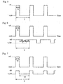
- Fig. 6 shows that: at a time when a voltage is applied in order to cause the organic EL element to emit luminescence and subsequently a time t2 passes, a reverse voltage is applied by a pulse wave for a time t3; and when a time t4 passes further, a voltage is again applied.
- Fig. 7 shows that over a time t5 when the voltage is not applied to the organic EL element, a DC reverse voltage is applied.
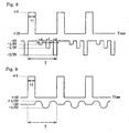
- Fig. 8 shows that when the voltage is not applied to the organic EL element, a reverse voltage is applied plural times by a pulse wave for a time t6, a time t7 and a time t8.
- the value of the reverse voltage is made higher as time passes. A fear that the organic luminescent medium is damaged by the reverse voltage becomes small.
- Fig. 9 shows that when the voltage is not applied to the organic EL element, a reverse voltage of an alternating wave is applied. It is also preferable to combine this alternating wave with the above-mentioned pulse wave appropriately, which is not illustrated.
- time t2 it is particularly preferable to set the time t2 to not less than 0 and not more than the luminous life span of the triplet-related luminous compound. This is particularly effective for removing the stored charge.
- a third embodiment is an organic EL display device comprising an organic EL element having a structure wherein an organic luminescent medium is sandwiched between a top electrode and a bottom electrode, and a driving circuit for driving the organic EL element, wherein the organic luminescent medium comprises a host compound and a triplet-related luminous compound; the driving circuit applies a electric pulse voltage or pulse current having a frequency of 30 Hz or more and a duty ratio of 1/5 or less; and further a hole barrier layer is arranged between the organic luminescent medium and the cathode.
- the hole barrier layer which is different from the first and second embodiments, is mainly described hereinafter.
- a compound having a larger ionization potential than the organic emitting layer it has been recognized that elements having the hole barrier layer particularly have the advantageous effect for removing stored charge. This is because the advantageous effect of the present invention is easily produced since charge is stored in the interface between the organic emitting layer and the hole barrier layer.
- Examples of compounds, which constitutes such hole barrier layer include phenanthroline derivatives represented by the following formulae (2) to (5): [In each of the formulae, R 1 to R 10 represent a hydrogen, a halogen atom, a hydroxyl group, NO 2 , CN, or a substituted or unsubstituted alkyl, aryl or amino group.]
- metal complexes having an 8-hydroxyquinoline derivative as a ligand are particularly preferable examples thereof.
- metal complexes having an energy gap of 2.8 eV or more are particularly preferable.
- the ionization potential of the hole barrier layer is larger than that of the organic luminescent medium.
- the ionization potential of the hole barrier layer 0.1 to 1 eV larger than that of the organic luminescent medium.
- the thickness of the hole barrier layer is not particularly limited.
- the thickness is preferably set into 1 nm to 1 ⁇ m.
- the thickness of the hole barrier layer is less than 1 nm, the luminescence brightness or durability may lower; and if the thickness of the hole barrier layer is more than 1 ⁇ m, the value of applying-voltage may become high.
- the thickness of the hole barrier layer is more preferably 3 nm to 500 nm, and still more preferably 5 nm to 100 nm.
- the method for forming the hole barrier layer is not particularly limited. It is preferable to form the layer by a method such as spin coating, casting or screen printing, or form the layer by a method such as sputtering, vapor deposition, chemical vapor deposition (CVD), or ion plating.
- An ITO film 130 nm in film thickness was formed on the whole of a glass substrate 112 mm long, 143 mm wide and 1.1 mm thick (OA2 glass, manufactured by Nippon Electric glass Co., Ltd.) by sputtering.
- a positive resist HRP 204 (manufactured by Fuji Hunt Electronics Technology Co., Ltd.) was applied onto this ITO film by spin coating, and the resultant was dried at a temperature of 80°C for 15 minutes.
- TMAH tetramethylammonium hydroxide
- an oven was used to conduct post baking treatment at a temperature of 130°C and subsequently an aqueous solution of hydrobromic acid (concentration: 47% by weight) was used as an etchant to etch the ITO film.
- a peeling solution N303 manufactured by Nagase & Co., Ltd. was used to remove the positive resist, thereby forming an ITO pattern in a stripe form (the number of lines: 960) as an anode (bottom electrode).
- an acrylic acid type negative resist V259 PA manufactured by Nippon Steal Chemical Co., Ltd.
- an acrylic acid type negative resist V259 PA was applied onto the ITO pattern by spin coating, and the resultant was dried at a temperature of 80°C for 15 minutes.
- contact exposure using a high-pressure mercury lamp as a light source was performed (exposure quantity: 300 mJ/cm 2 ) through a photo mask allowing the ITO to be exposed in the form of 70 ⁇ m ⁇ 290 ⁇ m rectangles.
- TMAH TMAH was used as a developing solution to perform development, and further an oven was used to conduct post baking treatment at a temperature of 160°C to form a first inter-insulator.
- a Novolak resin type negative resist ZPN 1100 (manufactured by Nippon Zeon Co., Ltd.) was applied onto the first inter-insulator by spin coating.
- the resultant was dried at a temperature of 80°C for 15 minutes, and then contact exposure using a high-pressure mercury lamp as a light source was performed (exposure quantity: 70 mJ/cm 2 ) through a photo mask giving a stripe-like pattern (line width: 20 ⁇ m, and gap width: 310 ⁇ m) crossing the ITO pattern, which was the bottom pattern.
- the resultant was baked at a temperature of 90°C for 15 minutes.
- TMAH TMAH was used as a developing solution to perform development, thereby forming a second inter-insulator (line width: 20 ⁇ m, gap width: 310 ⁇ m, and film thickness: 5 ⁇ m) as partition walls.
- the glass substrate on which the ITO pattern and so on were formed (which may be referred to merely as the glass substrate hereinafter), was washed with isopropyl alcohol and with ultraviolet rays, and subsequently this glass substrate was shifted to a dehydrating unit for carrying out a dehydrating step. That is, the glass substrate was put into a dry box provided with an inert gas (nitrogen) circulating section, a dew point controlling section, and a heating device section (hot plate).
- the hot plate was used to heat the glass substrate inside the dry box up to 60°C, and in this state dry nitrogen was introduced into the box while the dew point was lowered to -50°C.
- the glass substrate was allowed to stand still for about 2 hours, thereby removing moisture in the first and second inter-insulators and moisture adhering to the surface of the glass substrate and others.
- the heating of the hot plate was stopped so that the temperature of the glass substrate lowered to room temperature. Thereafter, the dew point was kept without exposing the glass substrate to the atmosphere and the glass substrate was fixed onto a substrate holder inside a vacuum deposition machine (manufactured by ULVAC Japan, Ltd.).
- the following materials were charged into a heating board made of molybdenum inside the vacuum deposition machine.
- the vacuum degree of the vacuum deposition machine was reduced to 665 ⁇ 10 -7 Pa (5 ⁇ 10 -7 Torr), and layers-were laminated by vacuum drawing one time without breaking the vacuum state in the middle from the formation of a hole transport layer to the formation of a cathode, so as to form an organic luminescent medium and so on so that a vapor deposition rate and film thickness were as follows:
- a sealing glass substrate blue sheet glass, manufactured by Geomatec Co., Ltd.
- a sealing unit in which dry nitrogen was introduced, and the surrounding thereof was air-tightly covered with a photo-curable type adhesive agent TB 3102 (manufactured by Three Bond Co., Ltd.) to obtain an organic EL display device for measuring luminescence performance.
- a pulse current having a frequency of 60 Hz, a duty ratio of 1/10 and a current value of 24 mA/cm 2 was applied, from a driving circuit, between the bottom electrode (ITO pattern, anode) of the resultant organic EL display device and the top electrode (cathode) thereof, which was the counter electrode, so as to cause respective pixels (about 230000 pixels), which corresponded to cross points between the electrodes, to emit luminescence.
- a chroma meter CS 100 manufactured by Minolta Co., Ltd. was used to measure the luminescence brightness. As a result, a value of 500 cd/m 2 was obtained.
- the voltage necessary for giving the pulse current at this time was 10 V.
- the resultant organic EL display device was left in the atmosphere at room temperature (25°C), and continuously driven to measure the half life. As a result, the half life was 400 hours.
- the display device can be driven by a voltage of 10 V or less to make consumption power low and further the luminous life span can be made long by using the specific driving circuit.
- An organic EL element was formed and then a pulse current having a frequency of 60 Hz, a duty ratio of 1/10 and a current value of 20 mA/cm 2 was applied thereto from the driving circuit to make an evaluation in the same way as in Example 1 except that a hole barrier layer (film thickness: 10 nm) made of 2,9-dimethyl-4,7-diphenyl-1,10-phenanthroline was laid between the luminous layer and the electron injection layer of the organic EL display device in Example 1.
- a hole barrier layer film thickness: 10 nm
- the luminous brightness was 500 cd/m 2
- the half life was 400 hours.
- the organic EL element was evaluated in the same way as in Example 2 except that the duty ratio of the driving voltage in Example 2 was changed from 1/10 to 1/100, and a pulse current having a frequency of 60 Hz and a current value of 410 mA/cm 2 was applied from the driving circuit.
- the luminous brightness was 500 cd/m 2
- the half life was 400 hours.
- the duty ratio of the same driving voltage as in the element in Example 2 was changed from 1/10 to 1/100 and the frequency was changed from 60 Hz to 500 Hz. Furthermore, the organic EL element was evaluated in the same way as in Example 2 except that a pulse voltage (peak voltage: 14 V) was applied.
- the luminous brightness was 500 cd/m 2
- the half life was 460 hours.
- the organic EL element was evaluated in the same way as in Example 2 except that a reverse voltage of 1 V was applied when no luminescence was emitted, and a pulse current having a frequency of 60 Hz, a duty ratio of 1/10 and a current value of 20 mA/cm 2 was applied from the driving circuit.
- the luminous brightness was 500 cd/m 2
- the half life was 600 hours.
- the organic EL element was evaluated in the same way as in Example 2 except that the duty ratio of the driving voltage in Example 2 was changed from 1/10 to 1/7, and a pulse current having a frequency of 60 Hz and a current value of 12 mA/cm 2 was applied from the driving circuit.
- the luminous brightness was 500 cd/m 2
- the half life was 280 hours.
- the luminous brightness was 500 cd/m 2
- the half life was 3,000 hours.
- Example 2 a constant current value of 1.2 mA/cm 2 was applied from the driving circuit for evaluation.
- the luminous brightness was 500 cd/m 2
- the half life was 200 hours, which were about 50% of that in Examples 1 and 2.
- Example 2 a pulse current having a frequency of 50 Hz, a duty ratio of 1/4 and a current value of 5.8 mA/cm 2 was applied from the driving circuit for evaluation.
- the luminous brightness was 500 cd/m 2
- the half life was 200 hours, which were about 50% of that in Examples 1 and 2.
- the organic EL display device of the present invention even when a triplet-related luminous compound is used in its organic luminescent medium, consumption power can be made low and further the luminous life span thereof can be made long.
- the method for driving an organic EL display device of the present invention even when an organic EL display device using, in its organic luminescent medium, a triplet-related luminous compound is caused to emit luminescence, consumption power can be made low and further the luminous life span thereof can be made long.
Landscapes
- Engineering & Computer Science (AREA)
- Physics & Mathematics (AREA)
- Computer Hardware Design (AREA)
- General Physics & Mathematics (AREA)
- Theoretical Computer Science (AREA)
- Microelectronics & Electronic Packaging (AREA)
- Chemical & Material Sciences (AREA)
- Crystallography & Structural Chemistry (AREA)
- Materials Engineering (AREA)
- Optics & Photonics (AREA)
- Inorganic Chemistry (AREA)
- Electroluminescent Light Sources (AREA)
- Control Of Indicators Other Than Cathode Ray Tubes (AREA)
- Control Of El Displays (AREA)
Abstract
In an organic electroluminescence display
device(30) comprising an organic EL element (26)
having a structure wherein an organic luminescent
medium (24) is sandwiched between a top electrode
(20) and a bottom electrode (22), and a driving
circuit (14) for driving the organic EL element (26),
the organic luminescent medium (24) comprises a host
compound and a triplet-related luminous compound and
the driving circuit (14) applies a electric pulse
voltage or pulse current having a frequency of 30 Hz
or more and a duty ratio of 1/5 or ,less. In this way,
it is possible to provide an organic EL display
device which consumes a low electric power and has a
long luminous life span, and a method for driving
the same.
Description
This invention relates to an organic
electroluminescence display device (which may be
referred to as an organic EL display device
hereinafter), and a method for driving the same.
More specifically, the invention relates to an
organic EL display device which consumes a low
electric power and is capable of obtaining a long
luminous life span, and a method for driving the
same.
The "EL" described in the present specification
is an abbreviation of "electroluminescence".
Hitherto, there have been known simple driving
type organic EL display devices wherein an organic
EL element having an organic emitting layer
sandwiched between electrodes is driven by means of
an XY matrix electrode structure, and the devices
are disclosed in, for example, Japanese Patent
Application Laid-Open (JP-A) Nos. 2-37385 and 3-233891.
In such a simple driving type organic EL
luminous device, the so-called line sequential
scanning is performed. Therefore, in the case that
the number of scan lines is several hundred, the
instantaneous brightness required is several hundred
times observation brightness. Consequently, the
following problems are caused.
Therefore, in order to solve the problems which
simple driving type organic EL luminous devices have,
suggested is an active driving type organic EL
luminous device having a thin film transistor,
(which may be referred to as a TFT hereinafter), so
as to drive organic EL elements.
Such active driving type organic EL luminous
devices have characteristics that the driving
voltage thereof is largely lowered, the luminescence
efficiency is improved and further the consumption
power can be reduced with compared to simple driving
type organic EL luminous devices.
However, in the case that an active driving
type organic EL luminous device having such
advantageous effects has a compound having the light
emitting property to which the triplet state
contributes (hereinafter referred to as triplet-related
compound), for example, an organic
luminescent medium containing an iridium complex, a
high luminescence brightness is obtained whereas a
problem that the luminous life span is short is
encountered. That is, in triplet-related compounds,
the time when the molecules thereof are excited and
relaxed is longer in the case of compounds having
the light property related to the singlet state.
Hence, electric charge is stored inside, so that the
balance between holes and electrons is liable to be
destroyed. Thus, according to Japan Journal of
Applied Physics, Vol. 38, pp. L1502-L1504 (1999), in
the case of an organic EL luminous device having an
organic luminescent medium containing an iridium
complex, the luminescence efficiency thereof is a
value of 40 lumens/W or more under the condition
that the luminescence brightness is 500 cd/cm2 but
the half life thereof is a short time of 200 hours
or less.
Thus, the present inventors made eager
investigation on the above-mentioned problems. As a
result, it has been found out that an organic EL
display device which consumes a low electric power
and is drivable for a long time can be provided by
driving the device through an appropriately-set
driving circuit even if a combination of a host
compound with a triplet-related luminous compound is
used; accordingly, the display device can be applied
to the field of flat panel displays and others.
That is, an object of the present invention is
to provide an organic EL display device which
consumes a low electric power and gives a less drop
in luminescence brightness even when the device is
driven for a long time.
Another object of the present invention is to
provide a driving method capable of driving such an
organic EL display device at a low consumption power
for a long time.
According to the present invention, provided is
an organic EL display device comprising an organic
EL element having a structure wherein an organic
luminescent medium comprising a host compound and a
phosphorescent luminous compound is sandwiched
between a top electrode and a bottom electrode; and
a driving circuit for applying a electric pulse
current or pulse voltage having a frequency of 30 Hz
or more and a duty ratio of 1/5 or less so as to
drive the organic EL element.
The organic EL display device having such a
structure makes it possible to make consumption
power low even if a triplet-related luminous
compound is used, and further to make the luminous
life span thereof long.
In order to construct the present invention, it
is preferable that the present invention has a
driving circuit for applying the electric pulse
voltage or pulse current to cause the organic
luminescent medium to emit luminescence, and
subsequently applying a voltage (V2) in the
direction reverse to' that of the voltage (V1) of the
pulse wave applied between the electrodes of the
organic electroluminescence element.
The organic EL display device having such a
structure makes it possible to make the luminous
life span longer since electric charge stored inside
can be removed even when a triplet-related luminous
compound is used as the organic luminescent medium.
In order to construct the present invention, it
is preferable that the organic EL display device of
the present invention has a driving circuit for
applying the voltage (V2) which is a smaller than
the voltage (V1) of the pulse wave and is in the
direction reverse to that of the voltage (V1).
The organic EL display device having such a
structure makes it possible to make the luminous
life span still longer even when a triplet-related
luminous compound is used.
In order to construct the present invention, it
is preferable that the triplet-related luminous
compound is an organic metal complex.
The organic EL display device having such a
structure makes it possible to make consumption
power lower.
In order to construct the present invention, it
is preferable that the organic metal complex
comprises at least one metal selected from the group
consisting of Ir, Pt, Pd, Ru, Rh, Mo, Re, Pb and Bi.
The organic EL display device having such a
structure makes it possible to make consumption
power lower.
In order to construct the present invention, it
is preferable that the organic EL display device of
the present invention comprises a hole barrier layer
between the organic luminescent medium and the
cathode.
The organic EL display device having such a
structure makes it possible to make consumption
power lower even if a triplet-related luminous
compound is used, and further to make the luminous
life span longer.
In order to construct the present invention, it
is preferable that the hole barrier layer comprises
a phenanthroline derivative.
The organic EL display device having such a
structure makes it possible to make consumption
power lower even if a triplet-related luminous
compound is used, and further to make the luminous
life span longer.
In order to construct the present invention, it
is preferable that the driving circuit comprises a
thin film transistor for controlling the
luminescence of the organic EL element.
The organic EL display device having such a
structure makes it possible to make consumption
power lower even if a triplet-related luminous
compound is used, and further to make the luminous
life span longer.
Another aspect of the present invention is a
method for driving an organic luminescence display
device comprising an organic electroluminescence
element having a structure wherein an organic
luminescent medium is sandwiched between a top
electrode and a bottom electrode, comprising
applying a electric pulse current or pulse voltage
having a frequency of 30 Hz or more and a duty ratio
of 1/5 or less by means of a driving circuit, so as
to drive the organic electroluminescence element.
Preferably, the electric pulse current is applied.
By driving the organic EL display device in
this way, a low consumption power is attained even
when a triplet-related luminous compound is used,
and further'the luminous life span can be made
longer.
In order to carry out the driving method of the
present invention, it is preferable that the driving
circuit applies the electric pulse voltage or pulse
current to cause the organic luminescent medium to
emit luminescence, and subsequently applies a
voltage (V2) in the direction reverse to that of the
voltage (V1) of the pulse wave applied between the
electrodes of the organic electroluminescence
element.
By driving the organic EL display device in
this way, the luminous life span can be made longer
since electric charges stored inside can be
effectively removed even when a triplet-related
luminous compound is used.
Referred to the drawings, embodiments of the
present invention are specifically described
hereinafter. The drawings referred to merely
illustrate the size and the shape of respective
constituting elements and the arrangement
relationship therebetween schematically to such an
extent that this invention can be understood.
Accordingly, this invention is not limited to
illustrated examples only. In the drawings, hatching
representing a section may be omitted.
As illustrated in Fig. 1, an organic EL
luminous device of a first embodiment is an organic
EL display device 30 having an organic EL element 26
wherein an organic luminescent medium 24 is
sandwiched between a top electrode 20 and a bottom
electrode 22, which are set over a supporting
substrate 10, and a driving circuit 14 for driving
the organic EL element 26, wherein the organic
luminescent medium 24 comprises a host compound and
a triplet-related luminous compound, and further the
driving circuit 14 can apply an electric pulse
voltage (V1) or pulse current having a frequency of
30 Hz or more and a duty ratio of 1/5 or less, the
voltage (V1) being applied between the electrodes of
the organic EL element 26 at this time.
In Fig. 1, a TFT circuit is set up. However,
this TFT circuit may be omitted. Organic EL display
devices wherein a TFT circuit is set up are usually
driven by direct current whereas the above-mentioned
electric pulse voltage or pulse current is applied
in the present invention.
About the embodiment of the organic EL luminous
device of the present invention, constituting
elements thereof, the driving method thereof, and
others are described with reference to Fig. 1, and
other figures.
The support substrate in the organic EL display
device, (which may be referred to as the substrate
hereinafter), is a member for supporting the organic
EL element, the driving circuit, and others. It is
therefore preferable that the substrate is excellent
in mechanical strength and dimension stability.
Specific examples of such a substrate include a
glass plate, a metal plate, a ceramic plate or a
plastic plate (such as polycarbonate resin, acrylic
resin, vinyl chloride resin, polyethylene
terephthalate resin, polyimide resin, polyester
resin, epoxy resin, phenol resin, silicon resin or
fluorine-containing resin).
In order to avoid the invasion of moisture into
the organic EL display device, it is preferable to
subject the substrate made of these materials to
moisture proof treatment or hydrophobic treatment by
forming an inorganic film further or applying a
fluorine-containing resin.
Accordingly, in order to avoid the invasion of
moisture into the organic luminescent medium, it is
preferable to make the water content in the
substrate and the gas permeability coefficient
thereof small by moisture proofing treatment or
hydrophobic treatment. Specifically, it is
preferable to set the water content in the
supporting substrate and the gas permeability
coefficient into 0.0001% by weight or less and 1 ×
10-13 or less cc·cm/cm2·sec.cmHg, respectively.
The organic luminescent medium can be defined
as a medium containing an organic emitting layer
wherein an electron and a hole are recombined with
each other so that EL luminescence can be emitted.
This organic luminescent medium can be constructed,
for example, by laminating the following respective
layers on the bottom electrode. The triplet-related
luminous compound may be contained in any of the
following organic layers.
Examples of the luminous material (host
compound) in the organic luminescent medium include
only one or combinations of two or more selected
from carbazole derivatives, p-quaterphenyl
derivatives, p-quinquephenyl derivatives,
benzothiazole compounds, benzimidazole compounds,
benzoxazole compounds, metal-chelated oxynoid
compounds, oxadiazole compounds, styrylbenzene
compounds, distyrylpyrazine derivatives, butadiene
compounds, naphthalimide compounds, perylene
derivatives, aldazine derivatives, pyraziline
derivatives, cyclopentadiene derivatives,
pyrrolopyrrole derivatives, styrylamine derivatives,
coumarin compounds, aromatic dimethylidyne compounds,
metal complexes each having an 8-quinolinol
derivative as a ligand, and polyphenyl compounds.
Among these host compounds, more preferable are
4,4'-bis(2,2-di-t-butylphenylvinyl)biphenyl
(abbreviated to DTBPBBi), 4,4'-bis(2,2-diphenylvinyl)biphenyl
(abbreviated to DPVBi), and
derivatives thereof as the aromatic dimethylidyne
compounds.
The host compound is preferably a compound
having a larger singlet excitation energy than the
level of the triplet excitation energy obtained by
the triplet-related luminous compound so that the
host compound can use the triplet excitation energy,
and is more preferably a compound having a larger
triplet excitation energy than the energy level.
The phosphorescent luminous compound is a
compound which generates phosphorescence. It is
sufficient that the phosphorescent luminous compound
is a compound which has an excitation state life
span of 100 ns or more, and its life span can be
measured as a luminescence relaxation component. As
the method of measuring the life span, the time
dependent measurement of transit luminescent delay
can be used.
The phosphorescent luminous compound is
preferably a triplet-related compound wherein a
triplet state contributes to the step of emitting
luminescence. It is particularly preferable to use a
compound having at least one metal selected from the
group consisting of Ir, Pt, Pd, Ru, Rh, Mo, Re, Pb
and Bi as a central metal or central metals, and a
CN ligand having a skeleton structure represented by
the following formula (1), and a derivative thereof.
Preferable is also a complex having mixed ligands
wherein one CN ligand or two CN ligands are
coordinated and further one Lx (wherein Lx = OO, ON
or the like) is coordinated. Examples of the Lx
ligand include acetylacetone derivatives (acac) and
picoline derivatives (pic). Examples of such a
triplet-related luminous compound include only one
or combinations of two or more selected from an
iridium complex, a platinum complex, a palladium
complex, a ruthenium complex, a rubidium complex, a
molybdenum complex, and a rhenium complex.
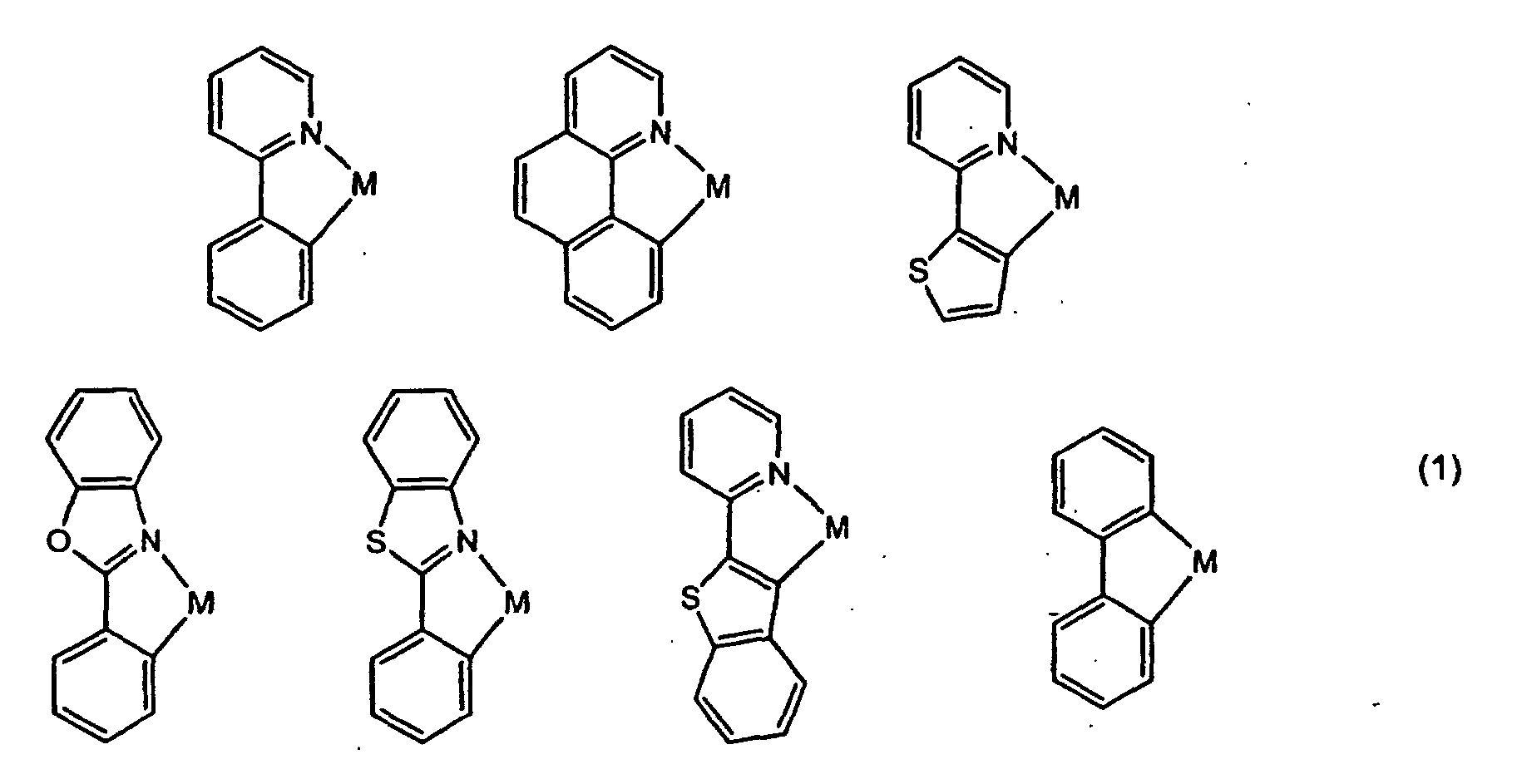
Among these triplet-related luminous compounds,
more specifically, the following are more
preferable: tris(2-phenylpyridyl)iridium
(abbreviated to Ir(ppy)3), bis(2-phenylpyridyl)platinum,
tris(2-phenylpyridyl)palladium,
tris(2-phenylpyridyl)ruthenium,
tris(2-phenylpyridyl)rubidium,
tris(2-phenylpyridyl)molybdenum,
Ir(ppy)2(acac),
Ir(btp)2(acac), BtpPt(acac), Ir(bo)2(acac),
Ir(bt)2(acac), Ir(ppy)2(Pic), and Ir(btp)2(pic).
This is because these triplet-related luminous
compounds can give luminescence property related to
the triplet state even at room temperature.
These complexes may have a substituent.
Examples of the substituent include alkyl groups,
fluorine, and aryl groups.
It is preferable to make the ionization
potential of the triplet-related luminous compound
larger than the ionization potential of the host
compound.
This is because such a triplet-related luminous
compound causes a hole transferred from the anode to
the organic emitting layer to be effectively held
inside the organic emitting layer so that the
luminescence efficiency can be made higher.
The amount of-the added triplet-related
luminous compound is preferably set into 0.1 to 50%
by weight of the total amount of the organic
luminescent medium.
This is because: if the amount of the added
triplet-related luminous compound is less than 0.1%
by weight, the effect of the addition may not be
exhibited; and if the amount of the added triplet-related
luminous compound is more than 50% by weight,
the half life may become excessively short.
Accordingly, the amount of the added triplet-related
luminous compound is more preferably set
into 1 to 30% by weight of the total amount of the
organic luminescent medium, and still more
preferably set into 5 to 20% by weight thereof.
Examples of hole transport material which
constitutes the hole transport layer include only
one or combinations of two or more selected from
triazole derivatives, oxadiazole derivatives,
imidazole derivatives, polyarylalkane derivatives,
pyrazoline derivatives, pyrazolone derivatives,
phenylenediamine derivatives, arylamine derivatives,
amino-substituted chalcone derivatives, oxazole
derivatives, fluorenone derivatives, hydrozone
derivatives, styrylanthracene derivatives, stylbene
derivatives, silazane derivatives, polysilane,
aniline-based copolymers, and conductive high-molecular
oligomer (in particular, thiophene
oligomer).
More specifically, it is particularly
preferable to use, among these hole transport
materials, a bis(diarylamino)arylene derivative
wherein the aryl is a polyphenyl and the arylene is
a polyphenylene since the life span thereof is
particularly long.
The polyphenyl is preferably biphenyl or
terphenyl, and the polyphenylene is preferably
biphenylyl or terphenylyl.
Examples of electron injection material which
constitutes the electron injection layer include
only one or combinations of two or more selected
from tris (8-quinolinolate) aluminum, tris(8-quinolinolate)
gallium, bis(10-benz[h]quinolinolate)
beryllium, triazole derivatives, oxadiazole
derivatives, triazine derivatives, perylene
derivatives, quinoline derivatives, quinoxaline
derivatives, diphenylquinone derivatives, nitro-substituted
fluorenone derivatives, thiopyrandioxide
derivatives.
It is also preferable to add the following as a
dopant to this electron injection material: an
alkali metal, alkali earth metal, rare earth metal,
alkali compound, alkali earth compound, rare earth
compound, or alkali metal to which an organic
compound coordinates.
The thickness of the organic luminescent medium
is not particularly limited. For example, the
thickness is preferably set into 5 nm to 5 µm.
This is because: if the thickness of the
organic luminescent medium is less than 5 nm, the
luminescence brightness or durability may lower;
whereas if the thickness of the organic luminescent
medium is more than 5 µm, the value of applying-voltage
may become high.
Accordingly, the thickness of the organic
luminescent medium is more preferably set into 10 nm
to 3 µm, and still more preferably set into 20 nm to
1 µm.
The top electrode and the bottom electrode are
described hereinafter. The top electrode and the
bottom electrode correspond to an anode layer and a
cathode layer, respectively, and a cathode layer and
an anode layer, respectively, correspondingly to the
structure of the organic EL element.
The bottom electrode corresponds to an anode
layer or a cathode layer, correspondingly to the
structure of the EL display device. For'example, in
the case that it corresponds to an anode layer, it
is preferable to use a metal, alloy or electrically
conductive compound which has a large work function
(for example, 4.0 eV or more), or a mixture thereof.
Specifically, it is preferable to use an electrode
material, such as indium tin oxide, indium zinc
oxide, strontium copper oxide, tin oxide, zinc oxide,
gold, platinum or palladium, alone, or use a
combination of two or more of these electrode
materials.
By using these electrode materials, the bottom
electrode which has a uniform thickness can be
formed by a method capable of forming a film in a
dry state, such as vapor deposition, sputtering, ion
plating, electron beam vapor deposition, CVD
(chemical vapor deposition), MOCVD (metal oxide
chemical vapor deposition), or plasma CVD (plasma
enhanced chemical vapor deposition).
Since EL luminescence has to be taken out from
the side of the bottom electrode in the present
invention, it is necessary to make the bottom
electrode to be a transparent electrode. It is
therefore preferable to use the above-mentioned
electrode material to set the transmittance of EL
luminescence into 70% or more.
The film thickness of the bottom electrode is
not particularly limited. For example, the thickness
is preferably set into 10 to 1,000 nm, and more
preferably set into 10 to 200 nm.
This is because a sufficient electric
conductivity is obtained and further a high
transmittance of 70% or more is obtained about EL
luminescence by setting the film thickness of the
bottom electrode into a value within such a range.
Meanwhile, the top electrode also corresponds
to an anode layer or a cathode layer,
correspondingly to the structure of the EL display
device. For example, in the case that it corresponds
to a cathode layer, it is preferable to use a metal,
alloy or electrically conductive compound which has
a smaller work function (for example, less than 4.0
eV) than the anode layer, or a mixture or inclusion
thereof.
Specifically, it is preferable to use an
electrode material, such as sodium, sodium-potassium
alloy, cesium, magnesium, lithium, magnesium-silver
alloy, aluminum, aluminum oxide, aluminum-lithium
alloy, indium, a rare earth metal, a mixture of
these metals and an organic luminescent medium
material, or a mixture of these metals and an
electron injection layer material, alone, or use a
combination of two or more of these electrode
materials.
The film thickness of the top electrode is not
particularly limited, either. Specifically, the
thickness is preferably set into 10 to 1,000 nm, and
more preferably set into 10 to 200 nm.
This is because a given sheet resistance and a
good electric connection reliability can be obtained
by setting the film thickness of the top electrode
into a value within such a range.
As illustrated in Fig. 1, the top electrode 20
is preferably composed of a main electrode 16, and
an auxiliary electrode 18 made of the material with
a lower resistivity.
Such a structure makes it possible to make the
sheet resistance of the top electrode 20 remarkably
low. Hence, the density of electric current flowing
through the organic luminescent medium can be
reduced. As a result, the life span of the organic
luminescent medium can be made remarkably long.
It is also preferable to lay a color converting
medium on the luminous surface of the organic EL
element. Examples of such a color converting medium
include a color filter, and a fluorescent film for
emitting light in color different from that of EL
luminescence. A combination thereof is also
preferable.
The color filter is set up to decompose or
filter light, thereby adjusting color or improving
contrast, and is made as a dye layer made of only a
dye, or as a lamellar matter made by dissolving or
dispersing a dye into a binder resin.
About the construction of the color filter, it
is preferable to contain dyes in blue, green and red.
This is because a combination of such a color filter
with an organic EL element which emits white
luminescence makes it possible to obtain the three
primary colors of light, blue, green and red, and
display full color.
It is preferable to use printing or
photolithography so as to pattern the color filter
in the same manner as in the case of a fluorescence
medium.
The fluorescent mediums in the organic EL
display device have a function of absorbing
luminescence of the organic EL element to emit
fluorescence having a longer wavelength, and are
made as a layer which are separately arranged in a
planar direction. Respective fluorescent medium
pieces are preferably arranged to correspond to
luminous areas of the organic EL element, for
example, positions of cross portions of the bottom
electrode and the top electrode. Such a structure
makes it possible that when the organic emitting
layer in the cross portions of the bottom electrode
and the top electrode emits luminescence, the
respective fluorescent medium pieces receive the
light and then luminescence in different colors
(wavelengths) can be taken out. In particular, such
a structure that the organic EL element emits blue
luminescence and further the luminescence can be
converted to green or red luminescence by the
fluorescent medium makes it possible that the three
primary colors of light, blue, green and red are
obtained even from the single organic EL element and
full-color display is attained. Thus, this structure
is preferable.
It is also preferable to arrange, between the
respective fluorescent medium pieces, a light
shielding layer (black matrix) for blocking
luminescence of the organic EL element and light
from the respective fluorescent medium pieces to
improve contrast and decrease the dependency on
field angle.
In order to prevent a fall in contrast by
external light, the fluorescent medium may be
constructed to be combined with the above-mentioned
color filter.
It is preferable to set the voltage value when
voltage is applied (or electric current is injected)
into 1 to 20 V.
This is because: if this voltage value is less
than 1 V, a desired luminescence brightness is not
obtained; whereas if this voltage value is more than
20 V, consumption power may be large.
Accordingly, the voltage value when voltage is
applied or electric current is injected is
preferably set into 3 to 15 V, and still more
preferably set into 8 to 13 V.
It is necessary that when voltage is applied or
electric current is injected, a pulse wave is used
and the frequency thereof is set into 30 Hz or more.
This is because if this frequency is less than
30 Hz, the resultant EL display flickers. However,
if the value of the frequency becomes excessively
large, a problem may be caused that deterioration of
the organic luminescent medium is promoted so that
the luminous life span falls.
Accordingly, the frequency when voltage is
applied or electric current is injected is
preferably set into 40 to 120 Hz, and more
preferably set into 50 to 100 Hz.
It is also necessary to set the duty ratio
(corresponding to t1/T in Fig. 5) of the pulse wave
when voltage is applied (or electric current is
injected), into 1/5 or less.
This is because if this duty ratio is more than
1/5, the half life of the organic EL display device
is short. However, if this duty ratio becomes
excessively small, a problem may be caused that the
luminescence brightness lowers.
Accordingly, the duty ratio when voltage is
applied or electric current is injected is
preferably set into 1/1000 to 1/10, and more
preferably set into 1/500 to 1/20.
Referring to Fig. 2, relationship between the
duty ratio and the half life is described herein in
more detail. As the transverse axis in Fig. 2, the
duty ratio (-) is taken and represented, and as the
vertical axis, the half life (Hrs) of the organic EL
display devices of Example 1 and others is taken and
represented.
As is easily understood from Fig. 2, the half
life tends to be shorter as the duty ratio is larger.
The duty ratio changes largely within a range that
the duty ratio is from 0.1 to 0.2. When the half
life, which is about 400 Hrs in the case that the
duty ratio is 0.1, exceeds 0.2, the half life falls
to about 200 Hrs. Conversely, if this duty ratio is
set into a value of 1/5 or less, that is, a value of
0.2 or less, a relatively long half life can be
obtained. If this duty ratio is set into a value of
0.1 or less, a longer half life can be obtained but
the value of the half life tends to be saturated.
Thus, the following conclusion can be obtained
from Fig. 2, as well: in order to obtain a long half
life, the duty ratio is indispensably set into 1/5
or less, preferably set into 1/1000 to 1/10, and
more preferably set into 1/500 to 1/20, as described
above. This result is a reason for daring to adopt
the above-mentioned duty ratio in active driving,
which is originally DC-driven.
As illustrated in Fig. 1, the organic EL
display device of the present invention preferably
has at least one TFT 14 and an organic EL element 26
driven by this TFT 14 on or over a supporting
substrate 10.
That is, an interlayer insulating film 13 and a
color converting medium 60, which are made flat, are
arranged between the TFT 14 and a bottom electrode
22 of the organic EL element 26, and a drain 47 of
the TFT 14 is electrically connected to the bottom
electrode 22 of the organic EL element 26 through an
electrically connecting member 28 placed in the
boundary between the interlayer insulating film 13
and the color converting medium 60.
As illustrated in a circuit diagram of Fig. 3
including a TFT and a layout plan of Fig. 4
including the TFT, to the TFT 14 are electrically
connected plural scan electrode lines (Yj to Yj+n)
50, (the number of which is n, and n is, for example,
from 1 to 1,000), and signal electrode lines (Xi to
Xi+n) 51, which are arranged in an XY matrix form.
Furthermore, common electrode lines (Ci to Ci+n) 52
laid in parallel to the signal electrode lines 51
are electrically connected to the TFT 14.
It is preferable that these electrode lines 50,
51 and 52 are electrically connected to the TFT 14
and they are combined with condensers 57 to
constitute electric switches for driving the organic
EL elements 26. In other words, it is preferable
that the electric switches are electrically
connected to the scan electrode lines 50, the signal
electrode lines 51 and others, and are further
composed of, for example, one or more first
transistors (which may be referred to as Tr1
hereinafter) 55, second transistors (which may be
referred to as Tr2 hereinafter) 56, and condensers
57.
It is preferable that the first transistor 55
has a function of selecting a luminous pixel and the
second transistor 56 has a function of driving an
organic EL element.
As illustrated in Fig. 1, an active layer 44 of
the first transistor (Tr1) 55 and the second
transistor (Tr2) 56 is composed of semiconductor
areas 45 and 47 doped into n type and a non-doped
semiconductor area 46, and can be represented by
n+/i/n+.
The semiconductor areas doped into the n type
become a source 45 and the drain 47, respectively,
and they are combined with a gate 43 provided to the
upper of the non-doped semiconductor area across a
gate oxide film 12 so as to constitute the
transistors 55 and 56 as a whole.
In the active layer 44, the semiconductor areas
45 and 47, which are doped into the n type, may be
doped into p type to make a structure of p+/i/p+.
The active layer 44 of the first transistor (Tr1) 55
and the second transistor (Tr2) 56 is preferably
made of an inorganic semiconductor such as
polysilicon, or an organic semiconductor such as
thiophene oligomer or poly (p-phenylenevinylene).
Polysilicon is a particularly preferable material
since it is more stable against electric conduction
than amorphous Si(α-Si).
The following describes a method for driving
organic EL elements based on a TFT. It is preferable
that this TFT includes the first transistor (Tr1) 55
and the second transistor (Tr2) 56 and further
constitutes an electric switch, as illustrated in
Fig. 3.
That is, the electric switch having such a
structure makes it possible to input a scan signal
pulse and a signal pulse through electrodes in an XY
matrix form and perform switching operation, thereby
driving the organic EL element 26.
More specifically, through the electric switch,
the organic EL element 26 is caused to emit light or
the light emission is stopped, whereby an image can
be displayed.
When the organic EL elements 26 are driven
through the electric switches in this way, a desired
one of the first transistors (Tr1) 55 is selected by
a scan pulse transmitted through the scan electrode,
lines (which may be referred to as gate lines) (Yj
to Yj+n) 50 and a scan pulse transmitted through the
signal electrode lines (Xi to Xi+n) 51, so that a
given electric charge is collected in one of the
condensers 57 formed between the common electrode
lines (Ci to Ci+n) 52 and the source 45 of the first
transistor (Tr1) 55.
In this way, the gate voltage of the second
transistor (Tr2) 56 turns to a constant value, so
that the second transistor (Tr2) 56 turns into an
ON-state. In this ON-state, the gate voltage is held
until a next gate pulse is transmitted. Accordingly,
electric current continues to be supplied to the
bottom electrode 22 of the organic EL element 26
connected to the drain 47 of the second transistor
(Tr2) 56.
Consequently, the organic EL element 26 can be
driven by the supplied electric current. Thus, the
driving voltage of the organic EL element 26 can be
largely lowered and the luminescence efficiency can
be improved. Moreover, the consumption power can be
reduced.
It is preferable to provide a sealing part to
the organic EL display device. It is preferable to
set such a sealing part onto the surrounding of the
organic EL display device in order to prevent the
invasion of moisture therein, or to insert a known
sealing medium, such as a drying agent, a dry gas,
or an inert gas such as fluorohydrocarbon, air-tightly
between the sealing part set in this way and
the organic EL display device.
This sealing part can be used as a supporting
substrate in the case that the fluorescent or the
color filter is set outside the top electrode.
As this sealing part, the same material as
constitutes the supporting substrate, for example, a
glass plate can be used. A thin film layer made of
oxide, oxynitride, nitride, sulfide or the like may
also be used. Preferred examples of this material
include SiOx (1 < x ≤ 2), SiOxNy (1 < x < 2, and 0 <
y < 1.5), AlOx (0.6 < x ≤ 1.5), AlON, SiAlON, SiC,
and SiCN. (x or y represents a composition ratio,
and SiAlON or the like, in which neither x nor y is
indicated, represents any composition ratio). The
form of the sealing part is not particularly limited.
The form is preferably made up, for example, to a
plate form or a cap form. For example, when the form
is made up to a plate form, the thickness thereof is
preferably set into 0.01 to 5 mm.
It is also preferable to make a groove or the
like in a part of the organic EL display device, and
push and fix the sealing part into it under pressure,
or to use a photo-curable type adhesive agent or the
like to fix the sealing part onto a part of the
organic EL display device.
A second embodiment is an organic EL display
device comprising an organic EL element having a
structure wherein an organic luminescent medium is
sandwiched between a top electrode and a bottom
electrode, and a driving circuit for driving the
organic EL element, wherein the organic luminescent
medium comprises a host compound and a triplet-related
luminous compound; the driving circuit
applies a electric pulse voltage or pulse current
having a frequency of 30 Hz or more and a duty ratio
of 1/5 or less; and further after the driving
circuit applies the electric pulse voltage or pulse
current to cause the organic luminescent medium to
emit luminescence, the driving circuit applies a
voltage (V2) in the direction reverse to that of the
voltage (V1) of the pulse wave applied between the
electrodes of the organic EL element.
About the second embodiment, conditions for
applying the reverse direction voltage, and others,
which are different from those in the first
embodiment, are mainly described hereinafter.
It is preferable that after the driving circuit
applies the electric pulse voltage or pulse current
to the organic luminescent medium so as to cause the
organic luminescent medium to emit luminescence,
that is, when the electric pulse voltage or pulse
current is not applied, the driving circuit applies
a voltage (V2) in the direction reverse to that of
the voltage (V1) of the pulse wave applied at the
time of emitting the luminescence. For example, in
the case that a plus-direction voltage is applied at
the time of emitting the luminescence, at the time
of not applying this voltage a minus-direction
voltage is applied to the organic luminescent medium.
By applying the voltage to the organic EL
display device in this way, the consumption power
can be made lower and the luminous life span can be
made longer even when the triplet-related luminous
compound is used. That is, the triplet-related
luminous compound has a problem that electric charge
is liable to be stored therein and thus the inner
electric field intensity thereof changes with the
passage of time and balance between holes and
electrons is broken, so that the luminescence
performance thereof changes easily. Thus, by
applying the reverse voltage in this way, the charge
stored in the triplet-related luminous compound can
be removed.
Hence, by applying the reverse voltage to the
organic luminescent medium, the problem of inner
storage of charge is overcome even if the triplet-related
luminous compound is used. As a result, the
consumption power is made lower and the luminous
life span can be made longer. In the case that
electric current is applied at the time of emitting
luminescence, the voltage necessary for giving the
electric current is defined as V1.
It is also preferable to set the reverse
voltage value when the electric pulse voltage or
pulse current is not applied into 0.01 to 15 V.
This is because if this reverse voltage value
is less than 0.01 V, the electric charge stored in
the triplet-related luminous compound is
insufficiently removed so that the effect of the
application of the reverse voltage may not be
obtained. On the other hand, if this reverse voltage
value is more than 15 V, the organic luminescent
medium may be deteriorated or destroyed.
Accordingly, the reverse voltage value is
preferably set into 0.1 to 10 V, and more preferably
set into 0.5 to 5 V.
For the application of the reverse voltage, a
direct current and an alternate current (which
includes a pulse wave), or either one thereof can be
used. The use of a pulse wave is preferable since
the electric charge stored in the triplet-related
luminous compound can be effectively removed.
About the electric current, a direct current
and an alternate current (which includes a pulse
wave), or either one thereof can be used.
It is preferable to decide the absolute value
(V2) of the reverse voltage, considering the value
of the voltage (V1) applied when the organic
luminescent medium emits luminescence. That is, the
absolute value (V2) of the reverse voltage is
preferably set into 1 to 90% of the voltage (V1)
applied when the organic luminescent medium emits
luminescence.
This is because if this absolute value of the
reverse voltage is less than 1% of the V1, the
electric charge stored in the triplet-related
luminous compound is insufficiently removed so that
the effect of the application of the reverse voltage
may not be obtained.
On the other hand, if the absolute value of the
reverse voltage is more than 90% of the V1, the
organic luminescent medium may be deteriorated or
destroyed.
Accordingly, this absolute value of the reverse
voltage is preferably set into 5 to 80% of the V1,
and more preferably set into 10 to 50% thereof.
When the reverse voltage is applied, it is
preferable to use a pulse wave, as well. In this
case, the frequency of the pulse wave is preferably
set into 10 to 120 Hz.
This is because if this frequency is less than
10 Hz, a problem may be caused that the stored
charge is insufficiently removed. On the other hand,
if this frequency is more than 120 Hz, deterioration
of the organic luminescent medium is promoted so
that the luminous life span may decrease.
Accordingly, the frequency of the pulse wave of
the reverse voltage is preferably set into 20 to 100
Hz, and more preferably set into 30 to 80 Hz.
The duty ratio of the pulse wave when the
reverse voltage is applied is preferably set into
1/20 to 1-the duty ratio of the pulse wave in the
forward direction.
This is because if this duty ratio is less than
1/20, the charge stored in the triplet-related
luminous compound is insufficiently removed so that
the effect of the application of the reverse voltage
may not be obtained.
On the other hand, this duty ratio cannot be
made larger than 1-the duty ratio of the pulse wave
in the forward direction.
Accordingly, the duty ratio of the pulse wave
when the reverse voltage is applied is preferably
set into the above-mentioned range, and more
preferably set into 1/10 to 90/100.
The timing when the reverse voltage is applied
is any other time than time when the electric pulse
voltage or pulse current is applied to cause the
organic EL element to emit luminescence. That is, if
the timing is any time when the voltage is not
applied, no especial problem is caused whether the
timing is any time when the organic EL element
continues to emit luminescence or any time when the
EL element emits no luminescence.
It is however preferable to apply the reverse
voltage in accordance with timing charts shown in
Figs. 6 to 9 since the charge stored in the triplet-related
luminous compound can be effectively removed
without promoting deterioration of the organic
luminescent medium.
That is, Fig. 6 shows that: at a time when a
voltage is applied in order to cause the organic EL
element to emit luminescence and subsequently a time
t2 passes, a reverse voltage is applied by a pulse
wave for a time t3; and when a time t4 passes
further, a voltage is again applied. Fig. 7 shows
that over a time t5 when the voltage is not applied
to the organic EL element, a DC reverse voltage is
applied.
Fig. 8 shows that when the voltage is not
applied to the organic EL element, a reverse voltage
is applied plural times by a pulse wave for a time
t6, a time t7 and a time t8. In the example shown in
Fig. 8, the value of the reverse voltage is made
higher as time passes. A fear that the organic
luminescent medium is damaged by the reverse voltage
becomes small.
Furthermore, Fig. 9 shows that when the voltage
is not applied to the organic EL element, a reverse
voltage of an alternating wave is applied. It is
also preferable to combine this alternating wave
with the above-mentioned pulse wave appropriately,
which is not illustrated.
It is particularly preferable to set the time
t2 to not less than 0 and not more than the luminous
life span of the triplet-related luminous compound.
This is particularly effective for removing the
stored charge.
A third embodiment is an organic EL display
device comprising an organic EL element having a
structure wherein an organic luminescent medium is
sandwiched between a top electrode and a bottom
electrode, and a driving circuit for driving the
organic EL element, wherein the organic luminescent
medium comprises a host compound and a triplet-related
luminous compound; the driving circuit
applies a electric pulse voltage or pulse current
having a frequency of 30 Hz or more and a duty ratio
of 1/5 or less; and further a hole barrier layer is
arranged between the organic luminescent medium and
the cathode.
The hole barrier layer, which is different from
the first and second embodiments, is mainly
described hereinafter.
It is preferable to use, as the compound which
constitutes the hole barrier layer, a compound
having a larger ionization potential than the
organic emitting layer. In the present invention, it
has been recognized that elements having the hole
barrier layer particularly have the advantageous
effect for removing stored charge. This is because
the advantageous effect of the present invention is
easily produced since charge is stored in the
interface between the organic emitting layer and the
hole barrier layer. Examples of compounds, which
constitutes such hole barrier layer include
phenanthroline derivatives represented by the
following formulae (2) to (5):
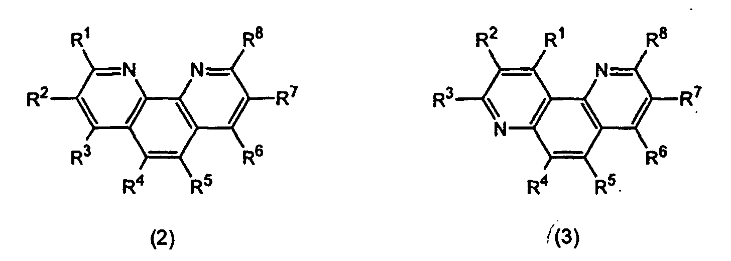
 [In each of the formulae, R1 to R10 represent a
hydrogen, a halogen atom, a hydroxyl group, NO2, CN,
or a substituted or unsubstituted alkyl, aryl or
amino group.]
[In each of the formulae, R1 to R10 represent a
hydrogen, a halogen atom, a hydroxyl group, NO2, CN,
or a substituted or unsubstituted alkyl, aryl or
amino group.]
Other preferable examples thereof are metal
complexes having an 8-hydroxyquinoline derivative as
a ligand. Particularly preferable are the metal
complexes having an energy gap of 2.8 eV or more.
In order to exhibit excellent hole barrier
property, it is preferable to make the ionization
potential of the hole barrier layer larger than that
of the organic luminescent medium.
In order to use a triplet-related luminous
compound in the organic emitting layer to improve
the luminescence efficiency, it is particularly
preferable to make the ionization potential of the
hole barrier layer 0.1 to 1 eV larger than that of
the organic luminescent medium.
The thickness of the hole barrier layer is not
particularly limited. For example, the thickness is
preferably set into 1 nm to 1 µm.
This is because: if the thickness of the hole
barrier layer is less than 1 nm, the luminescence
brightness or durability may lower; and if the
thickness of the hole barrier layer is more than 1 µm,
the value of applying-voltage may become high.
Accordingly, the thickness of the hole barrier
layer is more preferably 3 nm to 500 nm, and still
more preferably 5 nm to 100 nm.
The method for forming the hole barrier layer
is not particularly limited. It is preferable to
form the layer by a method such as spin coating,
casting or screen printing, or form the layer by a
method such as sputtering, vapor deposition,
chemical vapor deposition (CVD), or ion plating.
An ITO film 130 nm in film thickness was formed
on the whole of a glass substrate 112 mm long, 143
mm wide and 1.1 mm thick (OA2 glass, manufactured by
Nippon Electric glass Co., Ltd.) by sputtering. A
positive resist HRP 204 (manufactured by Fuji Hunt
Electronics Technology Co., Ltd.) was applied onto
this ITO film by spin coating, and the resultant was
dried at a temperature of 80°C for 15 minutes.
Next, contact exposure using a high-pressure
mercury lamp as a light source was performed through
a photo mask having a stripe-like pattern (line
width: 90 µm, and gap width: 20 µm) in such a manner
that the quantity of the exposure would be 100 mJ/cm2.
TMAH (tetramethylammonium hydroxide) was used as a
developing solution to perform development.
Next, an oven was used to conduct post baking
treatment at a temperature of 130°C and subsequently
an aqueous solution of hydrobromic acid
(concentration: 47% by weight) was used as an
etchant to etch the ITO film. Thereafter, a peeling
solution N303 (manufactured by Nagase & Co., Ltd.)
was used to remove the positive resist, thereby
forming an ITO pattern in a stripe form (the number
of lines: 960) as an anode (bottom electrode).
Next, an acrylic acid type negative resist V259
PA (manufactured by Nippon Steal Chemical Co., Ltd.)
was applied onto the ITO pattern by spin coating,
and the resultant was dried at a temperature of 80°C
for 15 minutes. Thereafter, contact exposure using a
high-pressure mercury lamp as a light source was
performed (exposure quantity: 300 mJ/cm2) through a
photo mask allowing the ITO to be exposed in the
form of 70 µm × 290 µm rectangles.
Next, TMAH was used as a developing solution to
perform development, and further an oven was used to
conduct post baking treatment at a temperature of
160°C to form a first inter-insulator.
Next, a Novolak resin type negative resist ZPN
1100 (manufactured by Nippon Zeon Co., Ltd.) was
applied onto the first inter-insulator by spin
coating. The resultant was dried at a temperature of
80°C for 15 minutes, and then contact exposure using
a high-pressure mercury lamp as a light source was
performed (exposure quantity: 70 mJ/cm2) through a
photo mask giving a stripe-like pattern (line width:
20 µm, and gap width: 310 µm) crossing the ITO
pattern, which was the bottom pattern. Next, the
resultant was baked at a temperature of 90°C for 15
minutes.
Next, TMAH was used as a developing solution to
perform development, thereby forming a second inter-insulator
(line width: 20 µm, gap width: 310 µm, and
film thickness: 5 µm) as partition walls.
Next, the glass substrate on which the ITO
pattern and so on were formed, (which may be
referred to merely as the glass substrate
hereinafter), was washed with isopropyl alcohol and
with ultraviolet rays, and subsequently this glass
substrate was shifted to a dehydrating unit for
carrying out a dehydrating step. That is, the glass
substrate was put into a dry box provided with an
inert gas (nitrogen) circulating section, a dew
point controlling section, and a heating device
section (hot plate).
The hot plate was used to heat the glass
substrate inside the dry box up to 60°C, and in this
state dry nitrogen was introduced into the box while
the dew point was lowered to -50°C. The glass
substrate was allowed to stand still for about 2
hours, thereby removing moisture in the first and
second inter-insulators and moisture adhering to the
surface of the glass substrate and others.
The heating of the hot plate was stopped so
that the temperature of the glass substrate lowered
to room temperature. Thereafter, the dew point was
kept without exposing the glass substrate to the
atmosphere and the glass substrate was fixed onto a
substrate holder inside a vacuum deposition machine
(manufactured by ULVAC Japan, Ltd.).
The following materials were charged into a
heating board made of molybdenum inside the vacuum
deposition machine.
Next, the vacuum degree of the vacuum
deposition machine was reduced to 665 × 10-7 Pa (5 ×
10-7 Torr), and layers-were laminated by vacuum
drawing one time without breaking the vacuum state
in the middle from the formation of a hole transport
layer to the formation of a cathode, so as to form
an organic luminescent medium and so on so that a
vapor deposition rate and film thickness were as
follows:
Next, a sealing glass substrate (blue sheet
glass, manufactured by Geomatec Co., Ltd.) was
laminated on the cathode inside a sealing unit in
which dry nitrogen was introduced, and the
surrounding thereof was air-tightly covered with a
photo-curable type adhesive agent TB 3102
(manufactured by Three Bond Co., Ltd.) to obtain an
organic EL display device for measuring luminescence
performance.
A pulse current having a frequency of 60 Hz, a
duty ratio of 1/10 and a current value of 24 mA/cm2
was applied, from a driving circuit, between the
bottom electrode (ITO pattern, anode) of the
resultant organic EL display device and the top
electrode (cathode) thereof, which was the counter
electrode, so as to cause respective pixels (about
230000 pixels), which corresponded to cross points
between the electrodes, to emit luminescence. A
chroma meter CS 100 (manufactured by Minolta Co.,
Ltd.) was used to measure the luminescence
brightness. As a result, a value of 500 cd/m2 was
obtained. The voltage necessary for giving the pulse
current at this time was 10 V.
Under the same conditions, the respective
pixels of the organic EL device were caused to emit
luminescence, and the CIE chromaticity thereof was
measured. As a result, it was proved that blue
luminescence wherein CIEx = 0.30 and CIEy = 0.63 in
CIE chromaticity coordinates was obtained.
Next, the resultant organic EL display device
was left in the atmosphere at room temperature (25°C),
and continuously driven to measure the half life. As
a result, the half life was 400 hours.
In conclusion, even if the organic luminescent
medium is doped with Ir (Ppy)3, which is a triplet-related
luminous compound, the display device can be
driven by a voltage of 10 V or less to make
consumption power low and further the luminous life
span can be made long by using the specific driving
circuit.
An organic EL element was formed and then a
pulse current having a frequency of 60 Hz, a duty
ratio of 1/10 and a current value of 20 mA/cm2 was
applied thereto from the driving circuit to make an
evaluation in the same way as in Example 1 except
that a hole barrier layer (film thickness: 10 nm)
made of 2,9-dimethyl-4,7-diphenyl-1,10-phenanthroline
was laid between the luminous layer
and the electron injection layer of the organic EL
display device in Example 1.
As a result, the luminous brightness was 500
cd/m2, and the CIE chromaticity was CIEx = 0.30 and
CIEy = 0.63. Furthermore, the half life was 400
hours.
That is, it was proved that by laying the hole
barrier layer, the half life, which was 400 hours,
did not change but the peak of the voltage was
lowered to 8 V to reduce consumption power.
The organic EL element was evaluated in the
same way as in Example 2 except that the duty ratio
of the driving voltage in Example 2 was changed from
1/10 to 1/100, and a pulse current having a
frequency of 60 Hz and a current value of 410 mA/cm2
was applied from the driving circuit.
As a result, the luminous brightness was 500
cd/m2, and the CIE chromaticity was CIEx = 0.30 and
CIEy = 0.63. Furthermore, the half life was 400
hours.
That is, by making the duty ratio small, the
current value instantaneously became far larger than
that in Example 2 but the half life, which was 400
hours, did not change. It is known that in drive
wherein the current value instantaneously becomes
large so that the duty ratio is large, the life span
usually becomes short. However, it was proved that
the life span can be kept.
The duty ratio of the same driving voltage as
in the element in Example 2 was changed from 1/10 to
1/100 and the frequency was changed from 60 Hz to
500 Hz. Furthermore, the organic EL element was
evaluated in the same way as in Example 2 except
that a pulse voltage (peak voltage: 14 V) was
applied.
As a result, the luminous brightness was 500
cd/m2, and the CIE chromaticity was CIEx = 0.30 and
CIEy = 0.63. Furthermore, the half life was 460
hours.
That is, it was proved that even when the duty
ratio was made small, the half life became 15%
larger than that in Examples 1 and 2 by making the
frequency large.
The organic EL element was evaluated in the
same way as in Example 2 except that a reverse
voltage of 1 V was applied when no luminescence was
emitted, and a pulse current having a frequency of
60 Hz, a duty ratio of 1/10 and a current value of
20 mA/cm2 was applied from the driving circuit.
As a result, the luminous brightness was 500
cd/m2, and the CIE chromaticity was CIEx = 0.30 and
CIEy = 0.63. Furthermore, the half life was 600
hours.
That is, it was proved that the half life
became 50% larger than that in Examples 1 and 2 by
applying the reverse voltage.
The organic EL element was evaluated in the
same way as in Example 2 except that the duty ratio
of the driving voltage in Example 2 was changed from
1/10 to 1/7, and a pulse current having a frequency
of 60 Hz and a current value of 12 mA/cm2 was applied
from the driving circuit.
As a result, the luminous brightness was 500
cd/m2, and the CIE chromaticity was CIEx = 0.30 and
CIEy = 0.63. Furthermore, the half life was 280
hours.
That is, it was proved that the current value
was lowered and the half life was lowered by making
the duty ratio somewhat large.
An organic EL element was formed and then a
pulse current having a frequency of 60 Hz, a duty
ratio of 1/10 and a current value of 18.5 mA/cm2 was
applied thereto from the driving circuit for
evaluation in the same way as in Example 2 except
that instead of NPD of the hole transport material
in Example 2, a bis(arylamino)biphenyl derivative
represented by the following formula (6) was used:

As a result, the luminous brightness was 500
cd/m2, and the CIE chromaticity was CIEx = 0.30 and
CIEy = 0.63. Furthermore, the half life was 3,000
hours.
In conclusion, it was proved that the half life
can be increased very largely by changing the kind
of the organic luminescent medium.
In Example 2, a constant current value of 1.2
mA/cm2 was applied from the driving circuit for
evaluation.
As a result, the luminous brightness was 500
cd/m2, and the CIE chromaticity was CIEx = 0.30 and
CIEy = 0.63. However, the half life was 200 hours,
which were about 50% of that in Examples 1 and 2.
In conclusion, it was proved that when the duty
ratio becomes excessively large (D = 1/1), the half
life becomes very low correspondingly.
In Example 2, a pulse current having a
frequency of 50 Hz, a duty ratio of 1/4 and a
current value of 5.8 mA/cm2 was applied from the
driving circuit for evaluation.
As a result, the luminous brightness was 500
cd/m2, and the CIE chromaticity was CIEx = 0.30 and
CIEy = 0.63. However, the half life was 200 hours,
which were about 50% of that in Examples 1 and 2.
In conclusion, it was proved that when the duty
ratio becomes excessively large (D = 1/4), the half
life becomes very low correspondingly.
According to the organic EL display device of
the present invention, even when a triplet-related
luminous compound is used in its organic luminescent
medium, consumption power can be made low and
further the luminous life span thereof can be made
long.
According to the method for driving an organic
EL display device of the present invention, even
when an organic EL display device using, in its
organic luminescent medium, a triplet-related
luminous compound is caused to emit luminescence,
consumption power can be made low and further the
luminous life span thereof can be made long.
Claims (11)
- An organic electroluminescence display device, comprising:an organic electroluminescence element having a structure wherein an organic luminescent medium comprising a host compound and a phosphorescent luminous compound is sandwiched between a top electrode and a bottom electrode; anda driving circuit for applying a electric pulse current or pulse voltage having a frequency of 30 Hz or more and a duty ratio of 1/5 or less so as to drive the organic electroluminescence element.
- The organic electroluminescence display device according to claim 1, wherein the phosphorescent luminous compound has a light emitting property to which triplet state contributes.
- The organic electroluminescence display device according to claim 1, wherein the driving circuit applies the electric pulse voltage or pulse current to cause the organic luminescent medium to emit luminescence, and subsequently applies a voltage (V2) in the direction reverse to that of the voltage (V1) of the pulse wave applied between the electrodes of the organic electroluminescence element.
- The organic electroluminescence display device according to claim 3, wherein the driving circuit applies the voltage (V2) which is a smaller than the voltage (V1) of the pulse wave and is in the direction reverse to that of the voltage (V1).
- The organic electroluminescence display device according to claim 1, wherein wherein the phosphorescent luminous compound having the light emitting property to which the triplet state contributes is an organic metal complex.
- The organic electroluminescence display device according to claim 5, wherein the organic metal complex comprises at least one metal selected from the group consisting of Ir, Pt, Pd, Ru, Rh, Mo, Re, Pb and Bi.
- The organic electroluminescence display device according to claim 1, which comprises a hole barrier layer between the organic luminescent medium and the cathode.
- The organic electroluminescence display device according to claim 7, wherein the hole barrier layer comprises a phenanthroline derivative.
- The organic electroluminescence display device according to claim 1, wherein the driving circuit comprises a thin film transistor for controlling the luminescence of the organic electroluminescence element.
- A method for driving an organic electroluminescence display device comprising an organic electroluminescence element having a structure wherein an organic luminescent medium is sandwiched between a top electrode and a bottom electrode, comprising:applying a electric pulse current or pulse voltage having a frequency of 30 Hz or more and a duty ratio of 1/5 or less by a driving circuit, so as to drive the organic electroluminescence element.
- The method for driving the organic electroluminescence display device according to claim 10, wherein the driving circuit applies the electric pulse voltage or pulse current to cause the organic luminescent medium to emit luminescence, and subsequently applies a voltage (V2) in the direction reverse to that of the voltage (V1) of the pulse wave applied between the electrodes of the organic electroluminescence element.
Applications Claiming Priority (3)
| Application Number | Priority Date | Filing Date | Title |
|---|---|---|---|
| JP2001242610 | 2001-08-09 | ||
| JP2001242610 | 2001-08-09 | ||
| PCT/JP2002/006889 WO2003017730A1 (en) | 2001-08-09 | 2002-07-08 | Organic electroluminescence display and its driving method |
Publications (2)
| Publication Number | Publication Date |
|---|---|
| EP1434469A1 true EP1434469A1 (en) | 2004-06-30 |
| EP1434469A4 EP1434469A4 (en) | 2006-08-09 |
Family
ID=19072857
Family Applications (1)
| Application Number | Title | Priority Date | Filing Date |
|---|---|---|---|
| EP02741433A Withdrawn EP1434469A4 (en) | 2001-08-09 | 2002-07-08 | ORGANIC ELECTROLUMINESCENT SCREEN AND METHOD OF CONTROLLING THE SAME |
Country Status (7)
| Country | Link |
|---|---|
| US (5) | US7034339B2 (en) |
| EP (1) | EP1434469A4 (en) |
| JP (2) | JP4613007B2 (en) |
| KR (1) | KR100841850B1 (en) |
| CN (1) | CN100440529C (en) |
| TW (1) | TW549007B (en) |
| WO (1) | WO2003017730A1 (en) |
Cited By (2)
| Publication number | Priority date | Publication date | Assignee | Title |
|---|---|---|---|---|
| US7521113B2 (en) | 2003-04-28 | 2009-04-21 | Zheng-Hong Lu | Light-emitting devices with fullerene layer |
| US9157023B2 (en) | 2003-11-18 | 2015-10-13 | Koninklijke Philips N.V. | Light-emitting device with an iridium complex |
Families Citing this family (39)
| Publication number | Priority date | Publication date | Assignee | Title |
|---|---|---|---|---|
| CN100440529C (en) * | 2001-08-09 | 2008-12-03 | 出光兴产株式会社 | Organic electroluminescent display device and driving method thereof |
| GB0120828D0 (en) * | 2001-08-28 | 2001-10-17 | Isis Innovation | Method of driving an electroluminescent device |
| JP3919583B2 (en) * | 2002-04-12 | 2007-05-30 | キヤノン株式会社 | Organic light emitting device |
| US9153168B2 (en) * | 2002-07-09 | 2015-10-06 | Semiconductor Energy Laboratory Co., Ltd. | Method for deciding duty factor in driving light-emitting device and driving method using the duty factor |
| JP3993117B2 (en) * | 2003-03-13 | 2007-10-17 | 日本放送協会 | Display drive circuit and image display device |
| WO2004086487A1 (en) * | 2003-03-26 | 2004-10-07 | Semiconductor Energy Laboratory Co. Ltd. | Semiconductor device and method for manufacturing same |
| KR100543003B1 (en) | 2003-09-15 | 2006-01-20 | 삼성에스디아이 주식회사 | Full color organic electroluminescent device and manufacturing method thereof |
| EP1521316B1 (en) | 2003-10-03 | 2016-05-25 | Semiconductor Energy Laboratory Co., Ltd. | Manufacturing method of a light emitting element |
| KR20050050487A (en) * | 2003-11-25 | 2005-05-31 | 삼성에스디아이 주식회사 | Full color organic electroluminescent device |
| KR100659530B1 (en) | 2003-11-26 | 2006-12-19 | 삼성에스디아이 주식회사 | Full Color Organic Light Emitting Diode |
| KR101110890B1 (en) * | 2004-04-02 | 2012-03-13 | 이데미쓰 고산 가부시키가이샤 | Organic electroluminescence element having two electroluminescent layers through electron barrier layer |
| JP4274070B2 (en) * | 2004-07-23 | 2009-06-03 | ソニー株式会社 | Display device and driving method thereof |
| US8248392B2 (en) * | 2004-08-13 | 2012-08-21 | Semiconductor Energy Laboratory Co., Ltd. | Light emitting device using light emitting element and driving method of light emitting element, and lighting apparatus |
| GB0422391D0 (en) * | 2004-10-08 | 2004-11-10 | Cambridge Display Tech Ltd | Light emitting device |
| JP5087815B2 (en) * | 2004-10-27 | 2012-12-05 | コニカミノルタホールディングス株式会社 | Organic EL device |
| ATE502395T1 (en) * | 2005-07-14 | 2011-04-15 | Koninkl Philips Electronics Nv | ELECTROLUMINescent LIGHT SOURCE |
| KR20070053060A (en) | 2005-11-19 | 2007-05-23 | 삼성전자주식회사 | Display device and manufacturing method thereof |
| KR101282399B1 (en) * | 2006-04-04 | 2013-07-04 | 삼성디스플레이 주식회사 | Display device and driving method thereof |
| EP2055149B1 (en) * | 2006-08-14 | 2017-04-19 | Philips Intellectual Property & Standards GmbH | Electroluminescent device having a variable color point |
| KR101293560B1 (en) | 2007-01-23 | 2013-08-06 | 삼성디스플레이 주식회사 | Display device and driving method thereof |
| KR100853540B1 (en) * | 2007-02-01 | 2008-08-21 | 삼성에스디아이 주식회사 | Organic light emitting display device and aging method |
| KR100858824B1 (en) * | 2007-05-31 | 2008-09-17 | 삼성에스디아이 주식회사 | Organic light emitting device and method for manufacturing same |
| JP5305637B2 (en) | 2007-11-08 | 2013-10-02 | キヤノン株式会社 | Organometallic complex, organic light emitting device using the same, and display device |
| JPWO2010046997A1 (en) * | 2008-10-24 | 2012-03-15 | 株式会社アドバンテスト | Electronic device and manufacturing method |
| CN102468414B (en) * | 2010-11-09 | 2014-08-13 | 四川新力光源股份有限公司 | Pulse LED (Light Emitting Diode) white light emitting device |
| US10199582B2 (en) * | 2013-09-03 | 2019-02-05 | University Of Southern California | Organic electroluminescent materials and devices |
| JP2015133362A (en) * | 2014-01-09 | 2015-07-23 | 三星ディスプレイ株式會社Samsung Display Co.,Ltd. | Organic electroluminescent element |
| JP6332557B2 (en) * | 2015-11-04 | 2018-05-30 | 住友化学株式会社 | Method for driving light emitting element and light emitting device |
| US10805538B2 (en) | 2015-12-16 | 2020-10-13 | Martineau & Associates, Inc. | Method and apparatus for remanent imaging control |
| CN108962127A (en) * | 2017-05-23 | 2018-12-07 | Tcl集团股份有限公司 | A kind of QLED device and its reverse drive mode |
| CN108962129A (en) * | 2017-05-23 | 2018-12-07 | Tcl集团股份有限公司 | A kind of QLED device and its backward voltage drive mode |
| CN108962130A (en) | 2017-05-23 | 2018-12-07 | Tcl集团股份有限公司 | It is a kind of to be driven in the reverse direction method applied to default in video display process |
| CN108962128A (en) * | 2017-05-23 | 2018-12-07 | Tcl集团股份有限公司 | A kind of QLED driving method based on square wave |
| CN108932926A (en) * | 2017-05-23 | 2018-12-04 | Tcl集团股份有限公司 | A kind of QLED device and its reversed driven mode |
| CN109064968A (en) * | 2017-05-23 | 2018-12-21 | Tcl集团股份有限公司 | A kind of driving method of active driving quantum dot display panel |
| CN108932925A (en) * | 2017-05-23 | 2018-12-04 | Tcl集团股份有限公司 | A kind of QLED driving method based on sine wave |
| CN108962133A (en) * | 2017-05-23 | 2018-12-07 | Tcl集团股份有限公司 | A kind of QLED device and its reverse current drive mode |
| KR102347796B1 (en) * | 2017-05-31 | 2022-01-07 | 엘지디스플레이 주식회사 | Electroluminescence display |
| CN112397014A (en) * | 2019-07-31 | 2021-02-23 | Tcl集团股份有限公司 | Drive method and drive device of quantum dot light-emitting diode and display device |
Family Cites Families (29)
| Publication number | Priority date | Publication date | Assignee | Title |
|---|---|---|---|---|
| JP2914981B2 (en) | 1988-07-27 | 1999-07-05 | パイオニア株式会社 | Display device |
| JP3016808B2 (en) | 1990-02-06 | 2000-03-06 | パイオニア株式会社 | Electroluminescent device and method of manufacturing the same |
| JP3169974B2 (en) | 1991-04-08 | 2001-05-28 | パイオニア株式会社 | Organic electroluminescent display device and driving method thereof |
| JP2998268B2 (en) * | 1991-04-19 | 2000-01-11 | 三菱化学株式会社 | Organic electroluminescent device |
| JPH07134558A (en) * | 1993-11-08 | 1995-05-23 | Idemitsu Kosan Co Ltd | Organic electroluminescence display device |
| GB9624706D0 (en) * | 1996-11-28 | 1997-01-15 | Cambridge Display Tech Ltd | Light emitting polymer device |
| JP3530362B2 (en) * | 1996-12-19 | 2004-05-24 | 三洋電機株式会社 | Self-luminous image display device |
| JPH10288965A (en) * | 1997-04-14 | 1998-10-27 | Casio Comput Co Ltd | Display device |
| JPH113048A (en) | 1997-06-10 | 1999-01-06 | Canon Inc | ELECTROLUMINESCENCE ELEMENT AND APPARATUS, AND ITS MANUFACTURING METHOD |
| US6413656B1 (en) * | 1998-09-14 | 2002-07-02 | The University Of Southern California | Reduced symmetry porphyrin molecules for producing enhanced luminosity from phosphorescent organic light emitting devices |
| JP3469764B2 (en) * | 1997-12-17 | 2003-11-25 | 三洋電機株式会社 | Organic electroluminescence device |
| GB9803441D0 (en) * | 1998-02-18 | 1998-04-15 | Cambridge Display Tech Ltd | Electroluminescent devices |
| JPH11354284A (en) * | 1998-06-10 | 1999-12-24 | Mitsubishi Chemical Corp | Organic electroluminescent device |
| JP5358050B2 (en) * | 1998-06-26 | 2013-12-04 | 出光興産株式会社 | Light emitting device |
| JP4505067B2 (en) * | 1998-12-16 | 2010-07-14 | 淳二 城戸 | Organic electroluminescent device |
| KR100913568B1 (en) * | 1999-05-13 | 2009-08-26 | 더 트러스티즈 오브 프린스턴 유니버시티 | Very high efficiency organic light emitting devices based on electrophosphorescence |
| TW527735B (en) * | 1999-06-04 | 2003-04-11 | Semiconductor Energy Lab | Electro-optical device |
| JP4730994B2 (en) * | 1999-06-04 | 2011-07-20 | 株式会社半導体エネルギー研究所 | Electro-optical device, manufacturing method thereof, and electronic device |
| JP4092857B2 (en) * | 1999-06-17 | 2008-05-28 | ソニー株式会社 | Image display device |
| TW483287B (en) * | 1999-06-21 | 2002-04-11 | Semiconductor Energy Lab | EL display device, driving method thereof, and electronic equipment provided with the EL display device |
| US6420057B1 (en) * | 1999-07-05 | 2002-07-16 | Konica Corporation | Organic electroluminescent element |
| US6310360B1 (en) * | 1999-07-21 | 2001-10-30 | The Trustees Of Princeton University | Intersystem crossing agents for efficient utilization of excitons in organic light emitting devices |
| JP2001085159A (en) * | 1999-09-13 | 2001-03-30 | Sanyo Electric Co Ltd | Organic electroluminescent element driving method, driving device, and display device using it |
| DE10003472C1 (en) | 2000-01-27 | 2001-04-26 | Infineon Technologies Ag | Random number generator on IC with significantly improved independence of both signals |
| TW532048B (en) * | 2000-03-27 | 2003-05-11 | Idemitsu Kosan Co | Organic electroluminescence element |
| GB2368844B (en) * | 2000-08-04 | 2004-07-07 | Chisso Corp | Organic electroluminescent device containing dithiafulvene derivative |
| JP2002100470A (en) * | 2000-09-22 | 2002-04-05 | Sanyo Electric Co Ltd | Driving method and driving device of organic electroluminescence element, and display device using them |
| CN100440529C (en) * | 2001-08-09 | 2008-12-03 | 出光兴产株式会社 | Organic electroluminescent display device and driving method thereof |
| TW559751B (en) * | 2001-08-24 | 2003-11-01 | Delta Optoelectronics Inc | Driving circuit and method of organic light-emitting diode |
-
2002
- 2002-07-08 CN CNB028156102A patent/CN100440529C/en not_active Expired - Lifetime
- 2002-07-08 KR KR1020047001911A patent/KR100841850B1/en not_active Expired - Lifetime
- 2002-07-08 JP JP2003521062A patent/JP4613007B2/en not_active Expired - Lifetime
- 2002-07-08 US US10/485,688 patent/US7034339B2/en not_active Expired - Lifetime
- 2002-07-08 WO PCT/JP2002/006889 patent/WO2003017730A1/en not_active Ceased
- 2002-07-08 EP EP02741433A patent/EP1434469A4/en not_active Withdrawn
- 2002-07-12 TW TW091115581A patent/TW549007B/en not_active IP Right Cessation
-
2006
- 2006-01-06 US US11/326,435 patent/US7956828B2/en not_active Expired - Fee Related
-
2010
- 2010-02-08 JP JP2010025308A patent/JP2010161385A/en active Pending
-
2011
- 2011-04-28 US US13/064,965 patent/US8471789B2/en not_active Expired - Fee Related
-
2013
- 2013-03-13 US US13/800,685 patent/US8654043B2/en not_active Expired - Fee Related
-
2014
- 2014-01-06 US US14/148,171 patent/US8902136B2/en not_active Expired - Fee Related
Cited By (2)
| Publication number | Priority date | Publication date | Assignee | Title |
|---|---|---|---|---|
| US7521113B2 (en) | 2003-04-28 | 2009-04-21 | Zheng-Hong Lu | Light-emitting devices with fullerene layer |
| US9157023B2 (en) | 2003-11-18 | 2015-10-13 | Koninklijke Philips N.V. | Light-emitting device with an iridium complex |
Also Published As
| Publication number | Publication date |
|---|---|
| JP2010161385A (en) | 2010-07-22 |
| JPWO2003017730A1 (en) | 2004-12-09 |
| CN100440529C (en) | 2008-12-03 |
| EP1434469A4 (en) | 2006-08-09 |
| US7034339B2 (en) | 2006-04-25 |
| US7956828B2 (en) | 2011-06-07 |
| US20130200346A1 (en) | 2013-08-08 |
| US20140138664A1 (en) | 2014-05-22 |
| US20040169622A1 (en) | 2004-09-02 |
| TW549007B (en) | 2003-08-21 |
| US8471789B2 (en) | 2013-06-25 |
| KR20040025743A (en) | 2004-03-25 |
| US20110205255A1 (en) | 2011-08-25 |
| KR100841850B1 (en) | 2008-06-27 |
| JP4613007B2 (en) | 2011-01-12 |
| US20060119279A1 (en) | 2006-06-08 |
| CN1541502A (en) | 2004-10-27 |
| US8654043B2 (en) | 2014-02-18 |
| US8902136B2 (en) | 2014-12-02 |
| WO2003017730A1 (en) | 2003-02-27 |
Similar Documents
| Publication | Publication Date | Title |
|---|---|---|
| US8902136B2 (en) | Organic electroluminescence display device and method for driving the same | |
| CN100364136C (en) | Organic Light Emitting Devices and Displays | |
| JP4048521B2 (en) | Light emitting element | |
| JP4298517B2 (en) | Organic light emitting device | |
| CN102714214B (en) | There is the OLED display architecture of the aperture ratio of improvement | |
| US20040222414A1 (en) | Organic electroluminescent element that suppresses generation of ultraviolet light and lighting system that has organic electroluminescent element | |
| EP1441573A2 (en) | Organic electroluminiscent device | |
| JP4181795B2 (en) | Electroluminescence element | |
| JP2008135498A (en) | Light emitting element | |
| JP2004185967A (en) | Organic electroluminescence element, method of manufacturing the same, display device, lighting device, and light source | |
| JP2006073581A (en) | Light emitting device material and light emitting device | |
| JP4089331B2 (en) | Light emitting element | |
| JP2004178896A (en) | Organic electroluminescence element and display device | |
| JPH07153576A (en) | Organic electroluminescent panel | |
| JP2005174675A (en) | Organic electroluminescent device and light emitting device | |
| JP3143350B2 (en) | Organic electroluminescence device | |
| JP2011065800A (en) | Organic el device, method of manufacturing the same, and electronic equipment equipped with this | |
| JPWO2005097941A1 (en) | ORGANIC ELECTROLUMINESCENT ELEMENT MATERIAL, ORGANIC ELECTROLUMINESCENT ELEMENT, DISPLAY DEVICE AND LIGHTING DEVICE | |
| JP4798138B2 (en) | Light emitting element | |
| JP2009043577A (en) | Color organic EL display and electronic device | |
| JP2009043576A (en) | Color organic EL display and electronic device | |
| JP2004164895A (en) | Organic electroluminescence element and display device |
Legal Events
| Date | Code | Title | Description |
|---|---|---|---|
| PUAI | Public reference made under article 153(3) epc to a published international application that has entered the european phase |
Free format text: ORIGINAL CODE: 0009012 |
|
| 17P | Request for examination filed |
Effective date: 20040129 |
|
| AK | Designated contracting states |
Kind code of ref document: A1 Designated state(s): AT BE CH CY DE DK ES FI FR GB GR IE IT LI LU MC NL PT SE TR |
|
| AX | Request for extension of the european patent |
Extension state: AL LT LV MK RO SI |
|
| A4 | Supplementary search report drawn up and despatched |
Effective date: 20060711 |
|
| 17Q | First examination report despatched |
Effective date: 20070420 |
|
| STAA | Information on the status of an ep patent application or granted ep patent |
Free format text: STATUS: THE APPLICATION IS DEEMED TO BE WITHDRAWN |
|
| 18D | Application deemed to be withdrawn |
Effective date: 20150203 |