EP1433221B1 - Waveguide in a printed circuit board - Google Patents
Waveguide in a printed circuit board Download PDFInfo
- Publication number
- EP1433221B1 EP1433221B1 EP02752720A EP02752720A EP1433221B1 EP 1433221 B1 EP1433221 B1 EP 1433221B1 EP 02752720 A EP02752720 A EP 02752720A EP 02752720 A EP02752720 A EP 02752720A EP 1433221 B1 EP1433221 B1 EP 1433221B1
- Authority
- EP
- European Patent Office
- Prior art keywords
- trench
- metalized
- bonding material
- printed circuit
- circuit board
- Prior art date
- Legal status (The legal status is an assumption and is not a legal conclusion. Google has not performed a legal analysis and makes no representation as to the accuracy of the status listed.)
- Expired - Lifetime
Links
- 239000000758 substrate Substances 0.000 claims abstract description 47
- 238000000034 method Methods 0.000 claims abstract description 26
- 239000000463 material Substances 0.000 claims description 43
- 239000002184 metal Substances 0.000 claims description 24
- 229910052751 metal Inorganic materials 0.000 claims description 24
- 239000003989 dielectric material Substances 0.000 claims description 7
- 239000004593 Epoxy Substances 0.000 claims description 6
- 239000011248 coating agent Substances 0.000 claims description 6
- 238000000576 coating method Methods 0.000 claims description 6
- 239000000853 adhesive Substances 0.000 claims description 4
- 230000001070 adhesive effect Effects 0.000 claims description 4
- 230000009969 flowable effect Effects 0.000 claims 1
- 238000010438 heat treatment Methods 0.000 claims 1
- 230000015572 biosynthetic process Effects 0.000 description 6
- 230000005540 biological transmission Effects 0.000 description 4
- 239000004020 conductor Substances 0.000 description 4
- 230000003287 optical effect Effects 0.000 description 4
- 238000001465 metallisation Methods 0.000 description 3
- 239000011347 resin Substances 0.000 description 3
- 229920005989 resin Polymers 0.000 description 3
- RYGMFSIKBFXOCR-UHFFFAOYSA-N Copper Chemical compound [Cu] RYGMFSIKBFXOCR-UHFFFAOYSA-N 0.000 description 2
- 239000004812 Fluorinated ethylene propylene Substances 0.000 description 2
- 239000002131 composite material Substances 0.000 description 2
- 238000010276 construction Methods 0.000 description 2
- 239000000835 fiber Substances 0.000 description 2
- 238000007747 plating Methods 0.000 description 2
- 229910052802 copper Inorganic materials 0.000 description 1
- 239000010949 copper Substances 0.000 description 1
- 239000011889 copper foil Substances 0.000 description 1
- 230000001419 dependent effect Effects 0.000 description 1
- 238000005553 drilling Methods 0.000 description 1
- 230000000694 effects Effects 0.000 description 1
- 238000005530 etching Methods 0.000 description 1
- 239000011888 foil Substances 0.000 description 1
- 239000011521 glass Substances 0.000 description 1
- 229910010272 inorganic material Inorganic materials 0.000 description 1
- 239000011147 inorganic material Substances 0.000 description 1
- 238000009413 insulation Methods 0.000 description 1
- 239000002648 laminated material Substances 0.000 description 1
- 238000010030 laminating Methods 0.000 description 1
- 238000003475 lamination Methods 0.000 description 1
- 238000010297 mechanical methods and process Methods 0.000 description 1
- 238000005459 micromachining Methods 0.000 description 1
- 239000011368 organic material Substances 0.000 description 1
- 150000003071 polychlorinated biphenyls Chemical class 0.000 description 1
- 230000000644 propagated effect Effects 0.000 description 1
- 238000001228 spectrum Methods 0.000 description 1
- 238000004544 sputter deposition Methods 0.000 description 1
Images


Classifications
-
- H—ELECTRICITY
- H05—ELECTRIC TECHNIQUES NOT OTHERWISE PROVIDED FOR
- H05K—PRINTED CIRCUITS; CASINGS OR CONSTRUCTIONAL DETAILS OF ELECTRIC APPARATUS; MANUFACTURE OF ASSEMBLAGES OF ELECTRICAL COMPONENTS
- H05K1/00—Printed circuits
- H05K1/02—Details
- H05K1/0213—Electrical arrangements not otherwise provided for
- H05K1/0237—High frequency adaptations
-
- H—ELECTRICITY
- H01—ELECTRIC ELEMENTS
- H01P—WAVEGUIDES; RESONATORS, LINES, OR OTHER DEVICES OF THE WAVEGUIDE TYPE
- H01P11/00—Apparatus or processes specially adapted for manufacturing waveguides or resonators, lines, or other devices of the waveguide type
- H01P11/001—Manufacturing waveguides or transmission lines of the waveguide type
- H01P11/002—Manufacturing hollow waveguides
-
- H—ELECTRICITY
- H05—ELECTRIC TECHNIQUES NOT OTHERWISE PROVIDED FOR
- H05K—PRINTED CIRCUITS; CASINGS OR CONSTRUCTIONAL DETAILS OF ELECTRIC APPARATUS; MANUFACTURE OF ASSEMBLAGES OF ELECTRICAL COMPONENTS
- H05K2201/00—Indexing scheme relating to printed circuits covered by H05K1/00
- H05K2201/03—Conductive materials
- H05K2201/0332—Structure of the conductor
- H05K2201/0364—Conductor shape
- H05K2201/037—Hollow conductors, i.e. conductors partially or completely surrounding a void, e.g. hollow waveguides
-
- H—ELECTRICITY
- H05—ELECTRIC TECHNIQUES NOT OTHERWISE PROVIDED FOR
- H05K—PRINTED CIRCUITS; CASINGS OR CONSTRUCTIONAL DETAILS OF ELECTRIC APPARATUS; MANUFACTURE OF ASSEMBLAGES OF ELECTRICAL COMPONENTS
- H05K2201/00—Indexing scheme relating to printed circuits covered by H05K1/00
- H05K2201/03—Conductive materials
- H05K2201/0332—Structure of the conductor
- H05K2201/0388—Other aspects of conductors
- H05K2201/0394—Conductor crossing over a hole in the substrate or a gap between two separate substrate parts
-
- H—ELECTRICITY
- H05—ELECTRIC TECHNIQUES NOT OTHERWISE PROVIDED FOR
- H05K—PRINTED CIRCUITS; CASINGS OR CONSTRUCTIONAL DETAILS OF ELECTRIC APPARATUS; MANUFACTURE OF ASSEMBLAGES OF ELECTRICAL COMPONENTS
- H05K2201/00—Indexing scheme relating to printed circuits covered by H05K1/00
- H05K2201/09—Shape and layout
- H05K2201/09009—Substrate related
- H05K2201/09036—Recesses or grooves in insulating substrate
-
- H—ELECTRICITY
- H05—ELECTRIC TECHNIQUES NOT OTHERWISE PROVIDED FOR
- H05K—PRINTED CIRCUITS; CASINGS OR CONSTRUCTIONAL DETAILS OF ELECTRIC APPARATUS; MANUFACTURE OF ASSEMBLAGES OF ELECTRICAL COMPONENTS
- H05K2201/00—Indexing scheme relating to printed circuits covered by H05K1/00
- H05K2201/09—Shape and layout
- H05K2201/09818—Shape or layout details not covered by a single group of H05K2201/09009 - H05K2201/09809
- H05K2201/09981—Metallised walls
-
- H—ELECTRICITY
- H05—ELECTRIC TECHNIQUES NOT OTHERWISE PROVIDED FOR
- H05K—PRINTED CIRCUITS; CASINGS OR CONSTRUCTIONAL DETAILS OF ELECTRIC APPARATUS; MANUFACTURE OF ASSEMBLAGES OF ELECTRICAL COMPONENTS
- H05K3/00—Apparatus or processes for manufacturing printed circuits
- H05K3/0011—Working of insulating substrates or insulating layers
- H05K3/0017—Etching of the substrate by chemical or physical means
Definitions
- the present Invention is directed to the field of printed circuit boards. More particularly, the present invention is directed to a method for forming and a structure comprising a waveguide for optical (and/or RF) transmission in a printed circuit board (or integrated circuit package).
- a printed circuit board is a composite of organic and inorganic materials with external and internal wiring that allows electronic components to be mechanically supported and electrically connected.
- a PUB may contain multiple insulation layers sandwiched between metal layers.
- a typical PCB contains at least one metal layer that is patterned to transfer signals between the electronic components, one power plane for distributing voltage throughout the PCB, and one ground plane.
- Shielded transmission lines may be used to ensure that high-speed signals and radio frequency (RF) signals are transmitted without interference or corruption by other signals, and to ensure that these signals do not emanate unwanted electronic emissions.
- One way of insulating or protecting these signals is to use shielded cable that includes a central conductor within a plastic dielectric material surrounded by a braided conductor. Although this construction is extremely effective in transmitting signals over a distance, it may require cumbersome interconnects, and may not be useful for transmitting signals over small distances such as on a printed circuit board, for example. Numerous methods have been employed to create a shielded signal path on printed circuit boards.
- Optical waveguides are another way to transmit signals.
- a waveguide transmits light or electromagnetic energy through an empty cavity or through a filled channel (as in glass or plastic fiber of a fiber optic cable).
- the waveguide may be coated with a highly reflective coating that causes the signal to be totally reflected from one side of the guide to the other.
- Waveguides may be used for communicating signals at all frequencies of the electromagnetic spectrum such as at radio frequencies and radar frequencies in addition to optical frequencies. It is desirable to form a waveguide within a printed circuit board so as to avoid problems caused by other transmission means and to enjoy the benefits of optical transmission.
- Embodiments of the present invention may be described with respect to substrates having a top surface and a bottom surface.
- a top surface and a bottom surface are merely exemplary of the figure drawing based on the orientation of the page. That is, a top surface in the figure drawings may not correspond to a top surface in actual use. It is intended that the terminology top and bottom are merely for reference with respect to the figure drawings.
- Embodiments of the present invention may provide a waveguide (or waveguide structure) in a printed circuit board or integrated circuit package. This may involve forming metalized trenches/channels in printed circuit board (PCB) laminate materials or within cured multi-layer PCBs. Embodiments of the present invention may also place/form a waveguide surface (i.e., a top wall of the waveguide) on bonding/adhesive material prior to laminating/bonding. The placement of the waveguide surface on the bonding material may be done by tack bonding, such as tack bonding a metal feature/strip to a b-stage side of a sheet of resin coded copper (RCC) foil, for example.
- PCB printed circuit board
- RRC resin coded copper
- inventions of the present invention may provide a method of forming a waveguide structure in a printed circuit board. This may include forming a trench in a substrate (such as a printed circuit board or a layer of a printed circuit board), providing at least one metalized surface along the trench, and applying a bonding surface having a metalized capping surface to the substrate such that the metalized capping surface is located over the trench having the at least one metalized surface so as to form the waveguide structure.
- the trench or channel may be formed in a dielectric material. That is, a channel/trench may be formed by selectively removing or displacing the dielectric material with any one of a number of well-known techniques such as by laser, photo-development, plasma or mechanical methods.
- the channel or trench may be formed along the path of the Intended waveguide.
- the channel/trench may then be metalized to provide conductive walls of the intended waveguide.
- a metalized capping surface may be created on a bonding material.
- This capping surface may be formed by selectively removing a metal layer from the bonding material, or selectively adding/placing metal/conductive surfaces onto the bonding material.
- the dielectric material (having the metalized channel) and the bonding material (having the metalized capping surface) may be bonded together to form the intended waveguide. This may be achieved by placing the metalized bonding material and the metalized channel together such that the waveguide surfaces align to form the intended waveguide structure.
- the waveguide structure may be completed by processing the aligned components through the required bonding cycle for the bonding material.
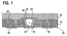
- Fig. 1 illustrates a waveguide structure provided within portions of a printed circuit board according to an example embodiment of the present invention. Other embodiments and configurations are also within the scope of the present invention. More particularly, Fig. 1 illustrates a first substrate 10 having a second substrate 20 mounted thereon. A waveguide (or waveguide structure) 30 is provided within the first substrate 10. In this embodiment, the waveguide 30 includes sidewalls 32 and 34, a top wall 36 and a bottom wall 38. The walls 32, 34, 36 and 38 may be reflective surfaces so as to enable the guiding of signals through the waveguide 30. The surfaces may also be electrically conductive.
- the waveguide 30 also includes an interior area 35 that may be filled with any material (such as resin) that is dissimilar to the material used in the forming of the walls 32, 34, 36 and 38 or the interior area 35 may contain air (i.e., an unfilled interior area).
- Fig. 1 additionally shows metal or conductive traces 42, 44, 46 located on the top and bottom surfaces of the substrate 10. Other metal traces are not labeled. Still further, the walls 32 and 34 may extend only partially through the material 10 and the wall 38 may be physically separated from the surface of the trace 44.
- FIG. 2-8 A method of forming the waveguide 30 in the printed circuit board will now be described with respect to Figs. 2-8 . That is, Figs. 2-8 represent various operations in the formation of the waveguide 30 according to an example embodiment of the present invention. Other operations and embodiments are also within the scope of the present invention.
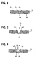
- Fig. 2 illustrates the first substrate 10 that may have the metal traces 42, 44, 46 (labeled in Fig. 1 ) and metal traces 43 and 45 (not labeled in Fig. 1 ) formed thereon.
- the substrate 10 may be a layered printed circuit board, for example. That is, the substrate 10 may correspond to a PCB laminated core.
- Fig. 3 illustrates a trench 50 (or channel) formed within the substrate 10.
- the trench 50 may be formed by any of a number of well-known manners such as mechanically (i.e., routing, drilling or stamping), chemically (i.e., dry or wet etch ) or electro-mechanically (i.e., laser or plasma).
- the metal traces 43 and 45 may be formed on a top surface of the substrate 10 at a location adjacent the top opening of the trench 50. As will be described below, the metal traces 43 and 45 may support a wall or surface of the waveguide 30.
- Fig. 4 illustrates metalization of three surfaces (or walls) within the trench 50. That is, Fig. 4 illustrates the metalized sidewall 32, the metalized sidewall 34, and the metalized bottom wall 38.
- the metalization of the wall(s) may be done in any of a number of well known manners including electroless, electrolytic and sputtering.
- Fig. 4 illustrates three walls of the trench 50, these walls may actually only correspond to one surface of the waveguide 30 or they may correspond to a plurality of surfaces of the waveguide 30. That is, surfaces of the trench 50 may be metalized to form three walls (shown in Fig. 4 ), or may be metalized to form one metalized wall or any number of walls. That is, one or a plurality of walls or surfaces may form the waveguide.
- the operations shown in Figs. 5A-5B show the formation of a metalized capping surface that may be placed on a top of the trench 50 (shown in Fig. 4 ) to form the top wall 36 of the waveguide 30.
- the operations shown in Figs. 6A-6C show another formation of the metalized capping surface that may be placed on a top of the trench 50 (shown in Fig. 4 ) to form the top wall 36 of the waveguide 30.
- the operations shown in Figs. 5A-5B and/or the operations shown in Figs. 6A-6C are all within the scope of the present invention. Other operations for forming the metalized capping surface are also within the scope of the present invention.
- Fig. 5A shows the formation of a waveguide surface (i.e., the top wall 36) on bonding material. This may involve providing the substrate 20, which may be a bonding material such as adhesive, epoxy, FEP, RCC or B-stage epoxy. A metal substrate (or surfaces) 60 may be placed on one surface (here the top surface) of the substrate 20.
- Fig. 5B shows the formation of a metalized surface 37 (corresponding to the top wall 36 of the waveguide 30).
- the metalized surface 37 is a metalized capping surface that may be aligned on the top of the trench 50 when the waveguide 30 is complete.
- the metalized surface 37 may be placed on the bonding material (i.e., the substrate 20) by tack bonding, plating or by any other well-known method.
- Figs. 6A-6C illustrate other operations for forming the metalized capping surface on bonding material.
- Fig. 6A shows the bonding material such as adhesive, epoxy, FEP, RCC or B-stage epoxy.
- Fig. 6B shows a metal coating 70 that may be applied to one surface (here the bottom surface) of the substrate 20. The metal coating 70 may be applied by plating or tacking to the substrate 20.
- Fig. 6C shows the formation of the metalized surface 37 (corresponding to the top wall 36 of the waveguide).
- the metalized surface 37 is the metalized capping surface that will be aligned on the top of the trench 50 when the waveguide 30 is complete. More specifically, Fig. 6C shows that portions of the metal coating 70 have been selectively removed so that only the metalized surface 37 remains.
- Fig. 7 illustrates the metalized surface 37 aligned with the metalized trench formed in the substrate 10.
- the metalized surface 37 forms the top wall 36 of the waveguide 30 by the placement and alignment of the substrate 20 over the substrate 10.
- the top wall 36 covers over the metal trace 43 and the metal trace 45 that are provided on the top of the substrate 10 just adjacent to the opening of the trench 50.
- the interior area 35 of the waveguide structure may be filled with resin, if desired.
- Fig. 7 further shows open areas 82 and 84 that may exist between the substrate 10 and the substrate 20 prior to any reflow of the bonding material.
- Fig. 8 shows the Fig. 7 structure after bonding/lamination of the aligned components. That is, Fig. 8 shows the result of reflow of the bonding material (that formed the substrate 20) in the areas 82 and 84. Adhesion of the bonding material around the edges of waveguide capping surface (i.e., the top wall 36) ensures that the waveguide structure is maintained and that the two components are bonded/laminated together.
- Fig. 8 may represent one layer (and bonding material) of a multi-layer printed circuit board or Fig. 8 may represent a plurality of layers of a printed circuit board. That is, Fig. 8 may not show the entire printed circuit board as other layers may also be formed and appropriately laminated together.
- Fig. 9 illustrates a flowchart 100 showing operations of embodiments of the present invention. Other embodiments, operations and orders of operation are also within the scope of the present invention. More particularly, an initial substrate (such as a dielectric material) is obtained in block 102. A trench may be formed in the substrate in block 104. This may correspond to the structures shown in Figs. 2 and 3 . Subsequently, a metalized surface or metalized surfaces may be formed within the trench in block 106. This may correspond to the metalization of the sidewalls and bottom wall as shown in Fig. 4 . In block 108, the metalized capping surface, which will be used to form the top wall of the waveguide structure, may be created. This may correspond to the operations shown in Figs.
- the metalized capping surface may be aligned over the initial substrate and the trench. This may correspond to the structure shown in Fig. 7 .
- the bonding material may be heated so as to affix the bonding material to the substrate. This may correspond to the structure shown in Fig. 8 . Accordingly, the method shown in the flowchart 100 forms at least one waveguide within a substrate of a printed circuit board.
- embodiments of the present invention may provide a method for forming a waveguide in a printed circuit board. This may include forming a trench in a substrate and forming at least one metalized surface along the trench. A metalized capping surface may be provided (or aligned) over the trench so as to form a waveguide structure.
- the walls of the waveguide may not be metal; but rather may be a material with a reflective surface to the waves being propagated.
- any reference in this specification to "one embodiment”, “an embodiment”, “example embodiment”, etc. means that a particular feature, structure, or characteristic described in connection with the embodiment is included in at least one embodiment of the invention.
- the appearances of such phrases in various places in the specification are not necessarily all referring to the same embodiment.
- certain method procedures may have been delineated as separate procedures; however, these separately delineated procedures should not be construed as necessarily order dependent in their performance. That is, some procedures may be able to be performed in an alternative ordering, simultaneously, etc.
Landscapes
- Engineering & Computer Science (AREA)
- Microelectronics & Electronic Packaging (AREA)
- Manufacturing & Machinery (AREA)
- Structure Of Printed Boards (AREA)
- Waveguides (AREA)
Abstract
Description
- The present Invention is directed to the field of printed circuit boards. More particularly, the present invention is directed to a method for forming and a structure comprising a waveguide for optical (and/or RF) transmission in a printed circuit board (or integrated circuit package).
- A printed circuit board (PCB) is a composite of organic and inorganic materials with external and internal wiring that allows electronic components to be mechanically supported and electrically connected. A PUB may contain multiple insulation layers sandwiched between metal layers. A typical PCB contains at least one metal layer that is patterned to transfer signals between the electronic components, one power plane for distributing voltage throughout the PCB, and one ground plane.
- Shielded transmission lines may be used to ensure that high-speed signals and radio frequency (RF) signals are transmitted without interference or corruption by other signals, and to ensure that these signals do not emanate unwanted electronic emissions. One way of insulating or protecting these signals is to use shielded cable that includes a central conductor within a plastic dielectric material surrounded by a braided conductor. Although this construction is extremely effective in transmitting signals over a distance, it may require cumbersome interconnects, and may not be useful for transmitting signals over small distances such as on a printed circuit board, for example. Numerous methods have been employed to create a shielded signal path on printed circuit boards.
- One option is to sandwich the signal conductor in the interior of the PCB between two outer ground planes. Unfortunately, this construction may only protect the signal conductor on the top and bottom sides but not the two lateral sides. In addition, this option may require considerable real estate on the PCB surfaces and significantly increase the laminate thickness.
- Optical waveguides are another way to transmit signals. A waveguide transmits light or electromagnetic energy through an empty cavity or through a filled channel (as in glass or plastic fiber of a fiber optic cable). The waveguide may be coated with a highly reflective coating that causes the signal to be totally reflected from one side of the guide to the other. Waveguides may be used for communicating signals at all frequencies of the electromagnetic spectrum such as at radio frequencies and radar frequencies in addition to optical frequencies. It is desirable to form a waveguide within a printed circuit board so as to avoid problems caused by other transmission means and to enjoy the benefits of optical transmission.
- In the article "Technique for micro-machining millimetrewave rectangular waveguide" of Collins C E et al, Electronics Letters, IEE Stevenage, GB, vol. 34, no. 10, 14 May 1998, pages 996-997, XP000846143, ISSN: 0013-5194, it is described that a pre-sputtered lid is attached to complete a waveguide.
US-B1-6,185,354 describes a printed circuit board with an integral waveguide having a metallic plate that provides the top of the waveguide that is formed directly to the waveguide channels. - The foregoing and a better understanding of the present invention will become apparent from the following detailed description of example embodiments and the claims when read in connection with the accompanying drawings, all forming a part of the disclosure of this invention. While the foregoing and following written and illustrated disclosure focuses on disclosing example embodiments of the invention, it should be clearly understood that the same is by way of illustration and example only and that the invention is not limited thereto.
- The following represents brief descriptions of the drawings in which like reference numerals represent like elements and wherein:
-
FIG. 1 shows a waveguide in a printed circuit board according to an example embodiment of the present invention; -
FIG. 2 illustrates a substrate having conductive traces; -
FIG. 3 illustrates a trench formed in the substrate ofFig. 2 ; -
FIG. 4 illustrates metalized surfaces in the trench ofFig. 3 ; -
FIG. 5A illustrates a bonding substrate having a metalized surface formed thereon; -
FIG. 5B illustrates theFig. 5A structure having a metalized capping surface formed thereon; -
FIG. 6A illustrates a bonding substrate; -
FIG. 6B illustrates a metalized surface on theFIG. 6A substrate; -
FIG. 6C illustrates a metalized capping surface formed from theFig. 6B structure; -
FIG. 7 illustrates a metalized capping surface and bonding substrate on theFIG. 4 structure; -
FIG. 8 illustrates a waveguide formed in a printed circuit board according to an example embodiment of the present invention; and -
FIG. 9 is a flowchart showing operations of a method according to an example embodiment of the present invention. - In the following detailed description, like reference numerals and characters may be used to designate identical, corresponding or similar components in differing figure drawings. Further, in the detailed description to follow, example embodiments may be described, although the present invention is not limited to the same. Where specific details are set forth in order to describe example embodiments of the invention, it should be apparent to one skilled in the art that the invention can be practiced without, or with variation of, these specific details.
- Embodiments of the present invention may be described with respect to substrates having a top surface and a bottom surface. One skilled in the art would understand that any reference to a top surface and a bottom surface are merely exemplary of the figure drawing based on the orientation of the page. That is, a top surface in the figure drawings may not correspond to a top surface in actual use. It is intended that the terminology top and bottom are merely for reference with respect to the figure drawings.
- Embodiments of the present invention may provide a waveguide (or waveguide structure) in a printed circuit board or integrated circuit package. This may involve forming metalized trenches/channels in printed circuit board (PCB) laminate materials or within cured multi-layer PCBs. Embodiments of the present invention may also place/form a waveguide surface (i.e., a top wall of the waveguide) on bonding/adhesive material prior to laminating/bonding. The placement of the waveguide surface on the bonding material may be done by tack bonding, such as tack bonding a metal feature/strip to a b-stage side of a sheet of resin coded copper (RCC) foil, for example. The tack bonding process may be utilized to join b-stage epoxy to other materials as one method to ensure alignment between circuit board layers. The placement of the waveguide surface on the bonding material may also be done by etching a copper foil previously adhered to a b-stage/c-stage composite. Accordingly, embodiments of the present invention may provide a method of forming a waveguide structure in a printed circuit board. This may include forming a trench in a substrate (such as a printed circuit board or a layer of a printed circuit board), providing at least one metalized surface along the trench, and applying a bonding surface having a metalized capping surface to the substrate such that the metalized capping surface is located over the trench having the at least one metalized surface so as to form the waveguide structure.
- More specifically, the trench or channel may be formed in a dielectric material. That is, a channel/trench may be formed by selectively removing or displacing the dielectric material with any one of a number of well-known techniques such as by laser, photo-development, plasma or mechanical methods. The channel or trench may be formed along the path of the Intended waveguide. The channel/trench may then be metalized to provide conductive walls of the intended waveguide.
- Subsequently, a metalized capping surface may be created on a bonding material. This capping surface may be formed by selectively removing a metal layer from the bonding material, or selectively adding/placing metal/conductive surfaces onto the bonding material.
- The dielectric material (having the metalized channel) and the bonding material (having the metalized capping surface) may be bonded together to form the intended waveguide. This may be achieved by placing the metalized bonding material and the metalized channel together such that the waveguide surfaces align to form the intended waveguide structure. The waveguide structure may be completed by processing the aligned components through the required bonding cycle for the bonding material.
- More specifically,
Fig. 1 illustrates a waveguide structure provided within portions of a printed circuit board according to an example embodiment of the present invention. Other embodiments and configurations are also within the scope of the present invention. More particularly,Fig. 1 illustrates afirst substrate 10 having asecond substrate 20 mounted thereon. A waveguide (or waveguide structure) 30 is provided within thefirst substrate 10. In this embodiment, thewaveguide 30 includes sidewalls 32 and 34, atop wall 36 and abottom wall 38. Thewalls waveguide 30. The surfaces may also be electrically conductive. Thewaveguide 30 also includes aninterior area 35 that may be filled with any material (such as resin) that is dissimilar to the material used in the forming of thewalls interior area 35 may contain air (i.e., an unfilled interior area).Fig. 1 additionally shows metal orconductive traces substrate 10. Other metal traces are not labeled. Still further, thewalls material 10 and thewall 38 may be physically separated from the surface of thetrace 44. - A method of forming the
waveguide 30 in the printed circuit board will now be described with respect toFigs. 2-8 . That is,Figs. 2-8 represent various operations in the formation of thewaveguide 30 according to an example embodiment of the present invention. Other operations and embodiments are also within the scope of the present invention. -
Fig. 2 illustrates thefirst substrate 10 that may have the metal traces 42, 44, 46 (labeled inFig. 1 ) and metal traces 43 and 45 (not labeled inFig. 1 ) formed thereon. Thesubstrate 10 may be a layered printed circuit board, for example. That is, thesubstrate 10 may correspond to a PCB laminated core. -
Fig. 3 illustrates a trench 50 (or channel) formed within thesubstrate 10. Thetrench 50 may be formed by any of a number of well-known manners such as mechanically (i.e., routing, drilling or stamping), chemically (i.e., dry or wet etch ) or electro-mechanically (i.e., laser or plasma). As shown inFig. 3 , the metal traces 43 and 45 may be formed on a top surface of thesubstrate 10 at a location adjacent the top opening of thetrench 50. As will be described below, the metal traces 43 and 45 may support a wall or surface of thewaveguide 30. -
Fig. 4 illustrates metalization of three surfaces (or walls) within thetrench 50. That is,Fig. 4 illustrates the metalizedsidewall 32, the metalizedsidewall 34, and the metalizedbottom wall 38. The metalization of the wall(s) may be done in any of a number of well known manners including electroless, electrolytic and sputtering. One skilled in the art would recognize that whileFig. 4 illustrates three walls of thetrench 50, these walls may actually only correspond to one surface of thewaveguide 30 or they may correspond to a plurality of surfaces of thewaveguide 30. That is, surfaces of thetrench 50 may be metalized to form three walls (shown inFig. 4 ), or may be metalized to form one metalized wall or any number of walls. That is, one or a plurality of walls or surfaces may form the waveguide. These embodiments are all within the scope of the present invention. - The operations shown in
Figs. 5A-5B show the formation of a metalized capping surface that may be placed on a top of the trench 50 (shown inFig. 4 ) to form thetop wall 36 of thewaveguide 30. The operations shown inFigs. 6A-6C show another formation of the metalized capping surface that may be placed on a top of the trench 50 (shown inFig. 4 ) to form thetop wall 36 of thewaveguide 30. The operations shown inFigs. 5A-5B and/or the operations shown inFigs. 6A-6C are all within the scope of the present invention. Other operations for forming the metalized capping surface are also within the scope of the present invention. -
Fig. 5A shows the formation of a waveguide surface (i.e., the top wall 36) on bonding material. This may involve providing thesubstrate 20, which may be a bonding material such as adhesive, epoxy, FEP, RCC or B-stage epoxy. A metal substrate (or surfaces) 60 may be placed on one surface (here the top surface) of thesubstrate 20.Fig. 5B shows the formation of a metalized surface 37 (corresponding to thetop wall 36 of the waveguide 30). The metalized surface 37 is a metalized capping surface that may be aligned on the top of thetrench 50 when thewaveguide 30 is complete. The metalized surface 37 may be placed on the bonding material (i.e., the substrate 20) by tack bonding, plating or by any other well-known method. Thesubstrate 20, thesubstrate 60 and
the metalized surface 37 may be placed onto the waveguide structure ofFig. 4 as will be described below.Figs. 6A-6C illustrate other operations for forming the metalized capping surface on bonding material. For example,Fig. 6A shows the bonding material such as adhesive, epoxy, FEP, RCC or B-stage epoxy.Fig. 6B shows ametal coating 70 that may be applied to one surface (here the bottom surface) of thesubstrate 20. Themetal coating 70 may be applied by plating or tacking to thesubstrate 20.Fig. 6C shows the formation of the metalized surface 37 (corresponding to thetop wall 36 of the waveguide). The metalized surface 37 is the metalized capping surface that will be aligned on the top of thetrench 50 when thewaveguide 30 is complete. More specifically,Fig. 6C shows that portions of themetal coating 70 have been selectively removed so that only the metalized surface 37 remains. -
Fig. 7 illustrates the metalized surface 37 aligned with the metalized trench formed in thesubstrate 10. The metalized surface 37 forms thetop wall 36 of thewaveguide 30 by the placement and alignment of thesubstrate 20 over thesubstrate 10. As may be seen, thetop wall 36 covers over themetal trace 43 and themetal trace 45 that are provided on the top of thesubstrate 10 just adjacent to the opening of thetrench 50. Prior to aligning thesubstrate 20 and the metalized surface 37 over thesubstrate 10, theinterior area 35 of the waveguide structure may be filled with resin, if desired.Fig. 7 further showsopen areas substrate 10 and thesubstrate 20 prior to any reflow of the bonding material. -
Fig. 8 shows theFig. 7 structure after bonding/lamination of the aligned components. That is,Fig. 8 shows the result of reflow of the bonding material (that formed the substrate 20) in theareas Fig. 8 may represent one layer (and bonding material) of a multi-layer printed circuit board orFig. 8 may represent a plurality of layers of a printed circuit board. That is,Fig. 8 may not show the entire printed circuit board as other layers may also be formed and appropriately laminated together. -
Fig. 9 illustrates aflowchart 100 showing operations of embodiments of the present invention. Other embodiments, operations and orders of operation are also within the scope of the present invention. More particularly, an initial substrate (such as a dielectric material) is obtained inblock 102. A trench may be formed in the substrate inblock 104. This may correspond to the structures shown inFigs. 2 and 3 . Subsequently, a metalized surface or metalized surfaces may be formed within the trench inblock 106. This may correspond to the metalization of the sidewalls and bottom wall as shown inFig. 4 . Inblock 108, the metalized capping surface, which will be used to form the top wall of the waveguide structure, may be created. This may correspond to the operations shown inFigs. 5A-5B or to the operations shown inFigs. 6A-6C . Inblock 110, the metalized capping surface may be aligned over the initial substrate and the trench. This may correspond to the structure shown inFig. 7 . Subsequently, inblock 112, the bonding material may be heated so as to affix the bonding material to the substrate. This may correspond to the structure shown inFig. 8 . Accordingly, the method shown in theflowchart 100 forms at least one waveguide within a substrate of a printed circuit board. - Accordingly, embodiments of the present invention may provide a method for forming a waveguide in a printed circuit board. This may include forming a trench in a substrate and forming at least one metalized surface along the trench. A metalized capping surface may be provided (or aligned) over the trench so as to form a waveguide structure.
- In another embodiment, the walls of the waveguide may not be metal; but rather may be a material with a reflective surface to the waves being propagated.
- Any reference in this specification to "one embodiment", "an embodiment", "example embodiment", etc., means that a particular feature, structure, or characteristic described in connection with the embodiment is included in at least one embodiment of the invention. The appearances of such phrases in various places in the specification are not necessarily all referring to the same embodiment. Further, when a particular feature, structure, or characteristic is described in connection with any embodiment, it is submitted that it is within the purview of one skilled in the art to effect such feature, structure, or characteristic in connection with other ones of the embodiments. Furthermore, for ease of understanding, certain method procedures may have been delineated as separate procedures; however, these separately delineated procedures should not be construed as necessarily order dependent in their performance. That is, some procedures may be able to be performed in an alternative ordering, simultaneously, etc.
Claims (14)
- A method comprising:forming a trench (50) in a substrate (10);forming two metal traces (43, 45) on a surface of the substrate (10) at a location adjacent to a top opening of the trench (50);providing at least one metalized surface (32, 34, 38) along said trench;aligning a metalized capping surface (37) on a bonding material (20) substantially only over said trench; andheating the bonding material (20) having the metalized capping surface (37) to affix said bonding material (20) to said substrate (10) such that said metalized capping surface (36, 37) is attached to said two metal traces (43, 45) and is located substantially only over said trench (50).
- The method of claim 1, wherein said substrate (10) comprises a printed circuit board.
- The method of claim 1, wherein said substrate (10) comprises a dielectric material.
- The method of claim 3, wherein said trench (50) is formed by selectively removing portions of said dielectric material.
- The method of claim 1, wherein said at least one metalized surface (32, 34, 38) comprises sidewall surfaces (32, 34) and a bottom surface (38) of a waveguide structure (30).
- The method of claim 1, wherein said metalized capping surface (37) on said bonding material (20) is formed by applying a metal coating (70) on said bonding material and selectively removing portions of said metal coating such that said metalized capping surface (37) remains on said bonding material (20) substantially only in places to be located over said trench (50).
- The method of claim 1, wherein said metalized capping surface (37) on said bonding material (20) is formed by selectively placing said metalized capping surface (36, 37) on said bonding material (20).
- The method of claim 1, further comprising filling said trench (50) with a material.
- A structure comprising:a printed circuit board (10), and a waveguide structure (30) provided within said printed circuit board, said waveguide structure including:a trench (35) within said printed circuit board (10);two metal traces (43, 45) formed on a surface of the printed circuit board (10)adjacent to a top opening of the trench (35); anda bonding material (20) having a capping surface (36) on at least a portion of said bonding material, the bonding material (20) disposed on top of said trench (35) with said capping surface (36) attached to said at least two metal traces (43, 45) and aligned substantially only over said trench (35),wherein said bonding material (20) is flowable when heated to affix said bonding material (20) to said printed circuit board (10).
- The structure of claim 9, wherein said trench (35) is within said printed circuit board (10) between a top surface of said printed circuit board and a bottom surface of said printed circuit board.
- The structure of claim 9, wherein said waveguide structure (30) includes material for walls (33, 34, 36, 38) of said waveguide structure such that said walls have reflective surfaces to enable guiding signals through said waveguide structure.
- The structure of claim 11, wherein said waveguide structure (30) comprises at least one metalized surface on at least one of a first sidewall, a second sidewall and a bottom wall and said capping surface is a metalized capping surface.
- The structure of claim 10, wherein said trench is filled with a material.
- The structure of claim 9, wherein the bonding material comprises a material selected from a list consisting of an epoxy and an adhesive.
Applications Claiming Priority (3)
| Application Number | Priority Date | Filing Date | Title |
|---|---|---|---|
| US963637 | 2001-09-27 | ||
| US09/963,637 US6882762B2 (en) | 2001-09-27 | 2001-09-27 | Waveguide in a printed circuit board and method of forming the same |
| PCT/US2002/025012 WO2003028147A1 (en) | 2001-09-27 | 2002-08-07 | Waveguide in a printed circuit board |
Publications (2)
| Publication Number | Publication Date |
|---|---|
| EP1433221A1 EP1433221A1 (en) | 2004-06-30 |
| EP1433221B1 true EP1433221B1 (en) | 2011-11-02 |
Family
ID=25507500
Family Applications (1)
| Application Number | Title | Priority Date | Filing Date |
|---|---|---|---|
| EP02752720A Expired - Lifetime EP1433221B1 (en) | 2001-09-27 | 2002-08-07 | Waveguide in a printed circuit board |
Country Status (5)
| Country | Link |
|---|---|
| US (1) | US6882762B2 (en) |
| EP (1) | EP1433221B1 (en) |
| CN (1) | CN1596485B (en) |
| AT (1) | ATE532231T1 (en) |
| WO (1) | WO2003028147A1 (en) |
Families Citing this family (35)
| Publication number | Priority date | Publication date | Assignee | Title |
|---|---|---|---|---|
| KR100483622B1 (en) * | 2002-08-16 | 2005-04-19 | 삼성전기주식회사 | Method for attaching optical waveguide component to printed circuit board |
| TWI282015B (en) * | 2003-08-22 | 2007-06-01 | Hon Hai Prec Ind Co Ltd | Process about a reflective film of a light guide plate |
| US20050063637A1 (en) * | 2003-09-22 | 2005-03-24 | Mershon Jayne L. | Connecting a component with an embedded optical fiber |
| US20050063638A1 (en) * | 2003-09-24 | 2005-03-24 | Alger William O. | Optical fibers embedded in a printed circuit board |
| KR20050076742A (en) * | 2004-01-22 | 2005-07-27 | 마츠시타 덴끼 산교 가부시키가이샤 | Fabrication method for optical transmission channel board, optical transmission channel board, board with built-in optical transmission channel, fabrication method for board with built-in optical transmission channel, and data processing apparatus |
| US20070145595A1 (en) * | 2005-12-27 | 2007-06-28 | Hall Stephen H | High speed interconnect |
| US20070154156A1 (en) * | 2005-12-30 | 2007-07-05 | Gary Brist | Imprinted waveguide printed circuit board structure |
| US20070154157A1 (en) * | 2005-12-30 | 2007-07-05 | Horine Bryce D | Quasi-waveguide printed circuit board structure |
| US20070274656A1 (en) * | 2005-12-30 | 2007-11-29 | Brist Gary A | Printed circuit board waveguide |
| US7480435B2 (en) * | 2005-12-30 | 2009-01-20 | Intel Corporation | Embedded waveguide printed circuit board structure |
| JP4711895B2 (en) * | 2006-02-03 | 2011-06-29 | ホシデン株式会社 | Photoelectric flexible wiring board connection structure, connector and photoelectric flexible wiring board |
| CN100510812C (en) * | 2006-11-09 | 2009-07-08 | 财团法人工业技术研究院 | Photoelectric substrate |
| US7800459B2 (en) * | 2006-12-29 | 2010-09-21 | Intel Corporation | Ultra-high bandwidth interconnect for data transmission |
| US20090041409A1 (en) * | 2007-08-06 | 2009-02-12 | Xyratex Technology Limited | electro-optical printed circuit board and a method of making an electro-optical printed circuit board |
| JP4928499B2 (en) * | 2008-05-14 | 2012-05-09 | 日東電工株式会社 | Suspension board with circuit |
| JP2010015641A (en) * | 2008-07-04 | 2010-01-21 | Nitto Denko Corp | Suspension board with circuit, and manufacturing method thereof |
| JP4989572B2 (en) * | 2008-07-07 | 2012-08-01 | 日東電工株式会社 | Suspension board with circuit and manufacturing method thereof |
| JP5374106B2 (en) * | 2008-09-26 | 2013-12-25 | ネオフォトニクス・セミコンダクタ合同会社 | Semiconductor optical functional device |
| JP5204738B2 (en) * | 2009-10-16 | 2013-06-05 | 日東電工株式会社 | Suspension board with circuit and manufacturing method thereof |
| JP5227940B2 (en) * | 2009-11-26 | 2013-07-03 | 日東電工株式会社 | Suspension board with circuit |
| CA2823965C (en) * | 2011-01-12 | 2017-11-07 | Research In Motion Limited | Printed circuit board with an acoustic channel for a microphone |
| US9544678B2 (en) * | 2011-01-12 | 2017-01-10 | Blackberry Limited | Printed circuit board with an acoustic channel for a microphone |
| US8748750B2 (en) | 2011-07-08 | 2014-06-10 | Honeywell International Inc. | Printed board assembly interface structures |
| US9142497B2 (en) | 2011-10-05 | 2015-09-22 | Harris Corporation | Method for making electrical structure with air dielectric and related electrical structures |
| US9144150B2 (en) | 2012-04-20 | 2015-09-22 | Xilinx, Inc. | Conductor structure with integrated via element |
| DE102013226066A1 (en) * | 2013-12-16 | 2015-06-18 | Siemens Aktiengesellschaft | Planar transformer and electrical component |
| CN113698488A (en) | 2014-09-12 | 2021-11-26 | 基因泰克公司 | Anti-B7-H4 antibodies and immunoconjugates |
| WO2016120254A1 (en) * | 2015-01-27 | 2016-08-04 | At & S Austria Technologie & Systemtechnik Aktiengesellschaft | Component carrier with integrated antenna structure |
| CN104795620B (en) * | 2015-04-10 | 2017-08-25 | 电子科技大学 | A kind of manufacture method of terahertz waveguide passive device |
| KR101927576B1 (en) * | 2016-01-18 | 2018-12-11 | 한국과학기술원 | Printed-circuit board having electromagnetic-tunnel-embedded arhchitecture and manufacturing method thereof |
| CN109075457B (en) | 2016-04-28 | 2021-08-31 | 奥特斯奥地利科技与系统技术有限公司 | Component carrier with integrated antenna arrangement, electronic device, radio communication method |
| US9947981B1 (en) | 2016-05-19 | 2018-04-17 | National Technology & Engineering Solutions of Sandian, LLC | Waveguide module comprising a first plate with a waveguide channel and a second plate with a raised portion in which a sealing layer is forced into the waveguide channel by the raised portion |
| DE102019200893B4 (en) * | 2019-01-21 | 2023-06-15 | Infineon Technologies Ag | Method of creating a waveguide, circuit device and radar system |
| US12119532B2 (en) * | 2019-12-20 | 2024-10-15 | 2Pi-Labs Gmbh | Waveguide arrangement |
| TWI772096B (en) * | 2021-07-07 | 2022-07-21 | 先豐通訊股份有限公司 | Circuit board having waveguides and method of manufacturing the same |
Family Cites Families (14)
| Publication number | Priority date | Publication date | Assignee | Title |
|---|---|---|---|---|
| US3150336A (en) | 1960-12-08 | 1964-09-22 | Ibm | Coupling between and through stacked circuit planes by means of aligned waeguide sections |
| US3157847A (en) | 1961-07-11 | 1964-11-17 | Robert M Williams | Multilayered waveguide circuitry formed by stacking plates having surface grooves |
| US5381596A (en) | 1993-02-23 | 1995-01-17 | E-Systems, Inc. | Apparatus and method of manufacturing a 3-dimensional waveguide |
| US5562838A (en) * | 1993-03-29 | 1996-10-08 | Martin Marietta Corporation | Optical light pipe and microwave waveguide interconnects in multichip modules formed using adaptive lithography |
| US6043861A (en) * | 1995-06-05 | 2000-03-28 | Motorola, Inc. | Optical waveguide using cholesteric liquid crystal polymer |
| US5617294A (en) * | 1995-09-29 | 1997-04-01 | Intel Corporation | Apparatus for removing heat from an integrated circuit package that is attached to a printed circuit board |
| JP3218996B2 (en) * | 1996-11-28 | 2001-10-15 | 松下電器産業株式会社 | Millimeter wave waveguide |
| US5929728A (en) | 1997-06-25 | 1999-07-27 | Hewlett-Packard Company | Imbedded waveguide structures for a microwave circuit package |
| US6000120A (en) * | 1998-04-16 | 1999-12-14 | Motorola, Inc. | Method of making coaxial transmission lines on a printed circuit board |
| US6185354B1 (en) | 1998-05-15 | 2001-02-06 | Motorola, Inc. | Printed circuit board having integral waveguide |
| DE19838519A1 (en) | 1998-08-25 | 2000-03-02 | Bosch Gmbh Robert | Optoelectronic printed circuit board, forms multilayer package with transparent layers |
| US6282358B1 (en) * | 1998-12-21 | 2001-08-28 | Lsi Logic Corporation | On-chip single layer horizontal deflecting waveguide and damascene method of fabricating the same |
| US6539157B2 (en) * | 2000-12-28 | 2003-03-25 | Honeywell Advanced Circuits, Inc. | Layered circuit boards and methods of production thereof |
| US6839478B2 (en) * | 2001-05-01 | 2005-01-04 | Terraop Ltd. | Optical switching system based on hollow waveguides |
-
2001
- 2001-09-27 US US09/963,637 patent/US6882762B2/en not_active Expired - Lifetime
-
2002
- 2002-08-07 EP EP02752720A patent/EP1433221B1/en not_active Expired - Lifetime
- 2002-08-07 AT AT02752720T patent/ATE532231T1/en active
- 2002-08-07 CN CN02823565.7A patent/CN1596485B/en not_active Expired - Fee Related
- 2002-08-07 WO PCT/US2002/025012 patent/WO2003028147A1/en not_active Ceased
Non-Patent Citations (1)
| Title |
|---|
| SAMPATH S K ET AL: "Rapid MEMS prototyping using SU-8, wafer bonding and deep reactive ion etching", PROCEEDINGS OF THE 14TH. BIENNIAL UNIVERSITY/GOVERNMENT/INDUSTRY MICROELECTRONICS. UGIM 2001. RICHMOND, VA, JUNE 17 - 20, 2001; [UNIVERSITY/GOVERNMENT/INDUSTRY MICROELECTRONICS SYMPOSIUM. (UGIM)], NEW YORK, NY : IEEE, US LNKD- DOI:10.1109/UGIM.2001.9, 17 June 2001 (2001-06-17), pages 158 - 161, XP010565239, ISBN: 978-0-7803-6691-6 * |
Also Published As
| Publication number | Publication date |
|---|---|
| CN1596485B (en) | 2010-12-01 |
| WO2003028147A1 (en) | 2003-04-03 |
| US6882762B2 (en) | 2005-04-19 |
| CN1596485A (en) | 2005-03-16 |
| ATE532231T1 (en) | 2011-11-15 |
| US20030059151A1 (en) | 2003-03-27 |
| EP1433221A1 (en) | 2004-06-30 |
Similar Documents
| Publication | Publication Date | Title |
|---|---|---|
| US6882762B2 (en) | Waveguide in a printed circuit board and method of forming the same | |
| EP3449532B1 (en) | Component carrier with integrated antenna arrangement, electronic apparatus, radio communication method | |
| CA2525620A1 (en) | Embedded rf vertical interconnect for flexible conformal antenna | |
| US7975378B1 (en) | Method of manufacturing high speed printed circuit board interconnects | |
| CN101527377B (en) | High-frequency equipment with rectangular waveguide | |
| CN111937230B (en) | Multilayer transmission line | |
| US8552815B2 (en) | High-frequency line structure for impedance matching a microstrip line to a resin substrate and method of making | |
| US20120292085A1 (en) | Flexible printed circuit and method of manufacturing the same | |
| US10219367B2 (en) | Multilayer resin substrate, and method of manufacturing multilayer resin substrate | |
| CN114144945A (en) | Flexible cable | |
| EP3659211A1 (en) | Antenna structure on high-frequency dielectric in cavity of component carrier | |
| WO2021230215A1 (en) | High frequency circuit | |
| US10219374B2 (en) | Printed wiring board | |
| JP3347607B2 (en) | Laminated waveguide line | |
| US20060285273A1 (en) | Composite distributed dielectric structure | |
| EP4060808A1 (en) | Component carrier with embedded high-frequency component and integrated waveguide for wireless communication | |
| CA2574208A1 (en) | Improved multi-layer integrated rf/if circuit board | |
| CN107926108B (en) | Radio frequency antenna, radio frequency substrate with radio frequency antenna and manufacturing method | |
| US7291916B2 (en) | Signal transmission structure and circuit substrate thereof | |
| CA2574211A1 (en) | Improved multi-layer integrated rf/if circuit board | |
| TWI823523B (en) | Circuit board and method for manufacturing the same | |
| CN113131165A (en) | Circuit structure | |
| TWI893545B (en) | Electromagnetic wave transmission board and method for fabricating the same | |
| KR20190111867A (en) | Flexible coil, and method of manufacturing the same, electronic component including flexible coil | |
| CN115767953B (en) | Soft-hard combined circuit board and manufacturing method thereof |
Legal Events
| Date | Code | Title | Description |
|---|---|---|---|
| PUAI | Public reference made under article 153(3) epc to a published international application that has entered the european phase |
Free format text: ORIGINAL CODE: 0009012 |
|
| 17P | Request for examination filed |
Effective date: 20040407 |
|
| AK | Designated contracting states |
Kind code of ref document: A1 Designated state(s): AT BE BG CH CY CZ DE DK EE ES FI FR GB GR IE IT LI LU MC NL PT SE SK TR |
|
| AX | Request for extension of the european patent |
Extension state: AL LT LV MK RO SI |
|
| 17Q | First examination report despatched |
Effective date: 20090721 |
|
| GRAP | Despatch of communication of intention to grant a patent |
Free format text: ORIGINAL CODE: EPIDOSNIGR1 |
|
| GRAS | Grant fee paid |
Free format text: ORIGINAL CODE: EPIDOSNIGR3 |
|
| GRAA | (expected) grant |
Free format text: ORIGINAL CODE: 0009210 |
|
| AK | Designated contracting states |
Kind code of ref document: B1 Designated state(s): AT BE BG CH CY CZ DE DK EE ES FI FR GB GR IE IT LI LU MC NL PT SE SK TR |
|
| REG | Reference to a national code |
Ref country code: GB Ref legal event code: FG4D |
|
| REG | Reference to a national code |
Ref country code: CH Ref legal event code: EP |
|
| REG | Reference to a national code |
Ref country code: IE Ref legal event code: FG4D |
|
| REG | Reference to a national code |
Ref country code: DE Ref legal event code: R096 Ref document number: 60241462 Country of ref document: DE Effective date: 20111229 |
|
| REG | Reference to a national code |
Ref country code: NL Ref legal event code: T3 |
|
| PG25 | Lapsed in a contracting state [announced via postgrant information from national office to epo] |
Ref country code: PT Free format text: LAPSE BECAUSE OF FAILURE TO SUBMIT A TRANSLATION OF THE DESCRIPTION OR TO PAY THE FEE WITHIN THE PRESCRIBED TIME-LIMIT Effective date: 20120302 Ref country code: GR Free format text: LAPSE BECAUSE OF FAILURE TO SUBMIT A TRANSLATION OF THE DESCRIPTION OR TO PAY THE FEE WITHIN THE PRESCRIBED TIME-LIMIT Effective date: 20120203 Ref country code: BE Free format text: LAPSE BECAUSE OF FAILURE TO SUBMIT A TRANSLATION OF THE DESCRIPTION OR TO PAY THE FEE WITHIN THE PRESCRIBED TIME-LIMIT Effective date: 20111102 Ref country code: SE Free format text: LAPSE BECAUSE OF FAILURE TO SUBMIT A TRANSLATION OF THE DESCRIPTION OR TO PAY THE FEE WITHIN THE PRESCRIBED TIME-LIMIT Effective date: 20111102 |
|
| PG25 | Lapsed in a contracting state [announced via postgrant information from national office to epo] |
Ref country code: CY Free format text: LAPSE BECAUSE OF FAILURE TO SUBMIT A TRANSLATION OF THE DESCRIPTION OR TO PAY THE FEE WITHIN THE PRESCRIBED TIME-LIMIT Effective date: 20111102 |
|
| PG25 | Lapsed in a contracting state [announced via postgrant information from national office to epo] |
Ref country code: DK Free format text: LAPSE BECAUSE OF FAILURE TO SUBMIT A TRANSLATION OF THE DESCRIPTION OR TO PAY THE FEE WITHIN THE PRESCRIBED TIME-LIMIT Effective date: 20111102 Ref country code: SK Free format text: LAPSE BECAUSE OF FAILURE TO SUBMIT A TRANSLATION OF THE DESCRIPTION OR TO PAY THE FEE WITHIN THE PRESCRIBED TIME-LIMIT Effective date: 20111102 Ref country code: EE Free format text: LAPSE BECAUSE OF FAILURE TO SUBMIT A TRANSLATION OF THE DESCRIPTION OR TO PAY THE FEE WITHIN THE PRESCRIBED TIME-LIMIT Effective date: 20111102 Ref country code: BG Free format text: LAPSE BECAUSE OF FAILURE TO SUBMIT A TRANSLATION OF THE DESCRIPTION OR TO PAY THE FEE WITHIN THE PRESCRIBED TIME-LIMIT Effective date: 20120202 Ref country code: CZ Free format text: LAPSE BECAUSE OF FAILURE TO SUBMIT A TRANSLATION OF THE DESCRIPTION OR TO PAY THE FEE WITHIN THE PRESCRIBED TIME-LIMIT Effective date: 20111102 |
|
| PG25 | Lapsed in a contracting state [announced via postgrant information from national office to epo] |
Ref country code: IT Free format text: LAPSE BECAUSE OF FAILURE TO SUBMIT A TRANSLATION OF THE DESCRIPTION OR TO PAY THE FEE WITHIN THE PRESCRIBED TIME-LIMIT Effective date: 20111102 |
|
| PLBE | No opposition filed within time limit |
Free format text: ORIGINAL CODE: 0009261 |
|
| STAA | Information on the status of an ep patent application or granted ep patent |
Free format text: STATUS: NO OPPOSITION FILED WITHIN TIME LIMIT |
|
| REG | Reference to a national code |
Ref country code: AT Ref legal event code: MK05 Ref document number: 532231 Country of ref document: AT Kind code of ref document: T Effective date: 20111102 |
|
| 26N | No opposition filed |
Effective date: 20120803 |
|
| REG | Reference to a national code |
Ref country code: DE Ref legal event code: R097 Ref document number: 60241462 Country of ref document: DE Effective date: 20120803 |
|
| PG25 | Lapsed in a contracting state [announced via postgrant information from national office to epo] |
Ref country code: AT Free format text: LAPSE BECAUSE OF FAILURE TO SUBMIT A TRANSLATION OF THE DESCRIPTION OR TO PAY THE FEE WITHIN THE PRESCRIBED TIME-LIMIT Effective date: 20111102 |
|
| REG | Reference to a national code |
Ref country code: NL Ref legal event code: V1 Effective date: 20130301 |
|
| REG | Reference to a national code |
Ref country code: CH Ref legal event code: PL |
|
| PG25 | Lapsed in a contracting state [announced via postgrant information from national office to epo] |
Ref country code: MC Free format text: LAPSE BECAUSE OF NON-PAYMENT OF DUE FEES Effective date: 20120831 |
|
| PG25 | Lapsed in a contracting state [announced via postgrant information from national office to epo] |
Ref country code: NL Free format text: LAPSE BECAUSE OF NON-PAYMENT OF DUE FEES Effective date: 20130301 Ref country code: LI Free format text: LAPSE BECAUSE OF NON-PAYMENT OF DUE FEES Effective date: 20120831 Ref country code: ES Free format text: LAPSE BECAUSE OF FAILURE TO SUBMIT A TRANSLATION OF THE DESCRIPTION OR TO PAY THE FEE WITHIN THE PRESCRIBED TIME-LIMIT Effective date: 20120213 Ref country code: CH Free format text: LAPSE BECAUSE OF NON-PAYMENT OF DUE FEES Effective date: 20120831 |
|
| REG | Reference to a national code |
Ref country code: FR Ref legal event code: ST Effective date: 20130430 |
|
| REG | Reference to a national code |
Ref country code: IE Ref legal event code: MM4A |
|
| PG25 | Lapsed in a contracting state [announced via postgrant information from national office to epo] |
Ref country code: FI Free format text: LAPSE BECAUSE OF FAILURE TO SUBMIT A TRANSLATION OF THE DESCRIPTION OR TO PAY THE FEE WITHIN THE PRESCRIBED TIME-LIMIT Effective date: 20111102 |
|
| PG25 | Lapsed in a contracting state [announced via postgrant information from national office to epo] |
Ref country code: IE Free format text: LAPSE BECAUSE OF NON-PAYMENT OF DUE FEES Effective date: 20120807 |
|
| PG25 | Lapsed in a contracting state [announced via postgrant information from national office to epo] |
Ref country code: FR Free format text: LAPSE BECAUSE OF NON-PAYMENT OF DUE FEES Effective date: 20120831 |
|
| PG25 | Lapsed in a contracting state [announced via postgrant information from national office to epo] |
Ref country code: TR Free format text: LAPSE BECAUSE OF FAILURE TO SUBMIT A TRANSLATION OF THE DESCRIPTION OR TO PAY THE FEE WITHIN THE PRESCRIBED TIME-LIMIT Effective date: 20111102 |
|
| PG25 | Lapsed in a contracting state [announced via postgrant information from national office to epo] |
Ref country code: LU Free format text: LAPSE BECAUSE OF NON-PAYMENT OF DUE FEES Effective date: 20120807 |
|
| PGFP | Annual fee paid to national office [announced via postgrant information from national office to epo] |
Ref country code: GB Payment date: 20160803 Year of fee payment: 15 Ref country code: DE Payment date: 20160802 Year of fee payment: 15 |
|
| REG | Reference to a national code |
Ref country code: DE Ref legal event code: R119 Ref document number: 60241462 Country of ref document: DE |
|
| GBPC | Gb: european patent ceased through non-payment of renewal fee |
Effective date: 20170807 |
|
| PG25 | Lapsed in a contracting state [announced via postgrant information from national office to epo] |
Ref country code: GB Free format text: LAPSE BECAUSE OF NON-PAYMENT OF DUE FEES Effective date: 20170807 Ref country code: DE Free format text: LAPSE BECAUSE OF NON-PAYMENT OF DUE FEES Effective date: 20180301 |