EP1432239A1 - Camera module - Google Patents
Camera module Download PDFInfo
- Publication number
- EP1432239A1 EP1432239A1 EP03029315A EP03029315A EP1432239A1 EP 1432239 A1 EP1432239 A1 EP 1432239A1 EP 03029315 A EP03029315 A EP 03029315A EP 03029315 A EP03029315 A EP 03029315A EP 1432239 A1 EP1432239 A1 EP 1432239A1
- Authority
- EP
- European Patent Office
- Prior art keywords
- camera module
- image sensor
- filter
- semiconductor chip
- filter portion
- Prior art date
- Legal status (The legal status is an assumption and is not a legal conclusion. Google has not performed a legal analysis and makes no representation as to the accuracy of the status listed.)
- Withdrawn
Links
Images


Classifications
-
- H—ELECTRICITY
- H10—SEMICONDUCTOR DEVICES; ELECTRIC SOLID-STATE DEVICES NOT OTHERWISE PROVIDED FOR
- H10F—INORGANIC SEMICONDUCTOR DEVICES SENSITIVE TO INFRARED RADIATION, LIGHT, ELECTROMAGNETIC RADIATION OF SHORTER WAVELENGTH OR CORPUSCULAR RADIATION
- H10F39/00—Integrated devices, or assemblies of multiple devices, comprising at least one element covered by group H10F30/00, e.g. radiation detectors comprising photodiode arrays
- H10F39/10—Integrated devices
- H10F39/12—Image sensors
-
- H—ELECTRICITY
- H10—SEMICONDUCTOR DEVICES; ELECTRIC SOLID-STATE DEVICES NOT OTHERWISE PROVIDED FOR
- H10F—INORGANIC SEMICONDUCTOR DEVICES SENSITIVE TO INFRARED RADIATION, LIGHT, ELECTROMAGNETIC RADIATION OF SHORTER WAVELENGTH OR CORPUSCULAR RADIATION
- H10F39/00—Integrated devices, or assemblies of multiple devices, comprising at least one element covered by group H10F30/00, e.g. radiation detectors comprising photodiode arrays
- H10F39/80—Constructional details of image sensors
- H10F39/804—Containers or encapsulations
-
- H—ELECTRICITY
- H04—ELECTRIC COMMUNICATION TECHNIQUE
- H04N—PICTORIAL COMMUNICATION, e.g. TELEVISION
- H04N23/00—Cameras or camera modules comprising electronic image sensors; Control thereof
- H04N23/50—Constructional details
- H04N23/54—Mounting of pick-up tubes, electronic image sensors, deviation or focusing coils
-
- H—ELECTRICITY
- H04—ELECTRIC COMMUNICATION TECHNIQUE
- H04N—PICTORIAL COMMUNICATION, e.g. TELEVISION
- H04N23/00—Cameras or camera modules comprising electronic image sensors; Control thereof
- H04N23/50—Constructional details
- H04N23/55—Optical parts specially adapted for electronic image sensors; Mounting thereof
-
- H—ELECTRICITY
- H10—SEMICONDUCTOR DEVICES; ELECTRIC SOLID-STATE DEVICES NOT OTHERWISE PROVIDED FOR
- H10F—INORGANIC SEMICONDUCTOR DEVICES SENSITIVE TO INFRARED RADIATION, LIGHT, ELECTROMAGNETIC RADIATION OF SHORTER WAVELENGTH OR CORPUSCULAR RADIATION
- H10F39/00—Integrated devices, or assemblies of multiple devices, comprising at least one element covered by group H10F30/00, e.g. radiation detectors comprising photodiode arrays
- H10F39/80—Constructional details of image sensors
- H10F39/806—Optical elements or arrangements associated with the image sensors
-
- H—ELECTRICITY
- H10—SEMICONDUCTOR DEVICES; ELECTRIC SOLID-STATE DEVICES NOT OTHERWISE PROVIDED FOR
- H10F—INORGANIC SEMICONDUCTOR DEVICES SENSITIVE TO INFRARED RADIATION, LIGHT, ELECTROMAGNETIC RADIATION OF SHORTER WAVELENGTH OR CORPUSCULAR RADIATION
- H10F77/00—Constructional details of devices covered by this subclass
- H10F77/40—Optical elements or arrangements
- H10F77/407—Optical elements or arrangements indirectly associated with the devices
-
- H—ELECTRICITY
- H10—SEMICONDUCTOR DEVICES; ELECTRIC SOLID-STATE DEVICES NOT OTHERWISE PROVIDED FOR
- H10F—INORGANIC SEMICONDUCTOR DEVICES SENSITIVE TO INFRARED RADIATION, LIGHT, ELECTROMAGNETIC RADIATION OF SHORTER WAVELENGTH OR CORPUSCULAR RADIATION
- H10F77/00—Constructional details of devices covered by this subclass
- H10F77/40—Optical elements or arrangements
- H10F77/413—Optical elements or arrangements directly associated or integrated with the devices, e.g. back reflectors
-
- H—ELECTRICITY
- H10—SEMICONDUCTOR DEVICES; ELECTRIC SOLID-STATE DEVICES NOT OTHERWISE PROVIDED FOR
- H10F—INORGANIC SEMICONDUCTOR DEVICES SENSITIVE TO INFRARED RADIATION, LIGHT, ELECTROMAGNETIC RADIATION OF SHORTER WAVELENGTH OR CORPUSCULAR RADIATION
- H10F77/00—Constructional details of devices covered by this subclass
- H10F77/50—Encapsulations or containers
-
- H—ELECTRICITY
- H10—SEMICONDUCTOR DEVICES; ELECTRIC SOLID-STATE DEVICES NOT OTHERWISE PROVIDED FOR
- H10W—GENERIC PACKAGES, INTERCONNECTIONS, CONNECTORS OR OTHER CONSTRUCTIONAL DETAILS OF DEVICES COVERED BY CLASS H10
- H10W99/00—Subject matter not provided for in other groups of this subclass
-
- H—ELECTRICITY
- H10—SEMICONDUCTOR DEVICES; ELECTRIC SOLID-STATE DEVICES NOT OTHERWISE PROVIDED FOR
- H10W—GENERIC PACKAGES, INTERCONNECTIONS, CONNECTORS OR OTHER CONSTRUCTIONAL DETAILS OF DEVICES COVERED BY CLASS H10
- H10W72/00—Interconnections or connectors in packages
- H10W72/20—Bump connectors, e.g. solder bumps or copper pillars; Dummy bumps; Thermal bumps
-
- H—ELECTRICITY
- H10—SEMICONDUCTOR DEVICES; ELECTRIC SOLID-STATE DEVICES NOT OTHERWISE PROVIDED FOR
- H10W—GENERIC PACKAGES, INTERCONNECTIONS, CONNECTORS OR OTHER CONSTRUCTIONAL DETAILS OF DEVICES COVERED BY CLASS H10
- H10W72/00—Interconnections or connectors in packages
- H10W72/50—Bond wires
- H10W72/531—Shapes of wire connectors
- H10W72/536—Shapes of wire connectors the connected ends being ball-shaped
Definitions
- This invention relates to a camera module, specifically to a small size camera module suitable to be incorporated into a portable device such as a mobile phone.
- FIG. 3 is a cross-sectional view showing a structure of such a camera module.
- Fig. 3 shows a lens-barrel 50, a lens 51 mounted inside the lens-barrel 50 and an IR filter 52 attached to a mouth of the lens-barrel 50 to block infrared radiation. It also shows an image sensor chip 60 housed in a space within the lens-barrel 50 and electrically connected with a printed circuit board 70.
- the image sensor chip 60 converts light incident from a photogenic subject through the IR filter 52 and the lens 51 into electric signals.
- a supporting glass substrate 62 is bonded to a thin silicon chip 61, in a surface of which CCDs (Charge Coupled Devices) are formed.
- CCDs Charge Coupled Devices
- Each of redistribution wirings 64A and 64B is formed to extend from each of electrode pads 63A and 63B, which are formed on a peripheral surface of the image sensor chip 60, over a side surface and to a back surface of the silicon chip 61.
- Each of the redistribution wirings 64A and 64B extends onto a glass substrate 65 which is bonded to the back surface of the silicon chip 61.
- Each of bump electrodes 66A and 66B is formed on an end of each of the redistribution wirings 64A and 64B extended onto the glass substrate 65.
- the bump electrodes 66A and 66B are connected to the printed circuit board 70.
- a DSP (Digital Signal Processor) 80 which performs video signal processing on the electric signals from the image sensor chip 60, is connected to a back surface of the printed circuit board 70 through bump electrodes 81A and 81B.
- the lens-barrel 50, the lens 51, the IR filter 52 and the image sensor chip 60 are discrete components, and the camera module is assembled by putting these discrete components together. This causes difficulty in reducing the size and production cost of the camera module.
- the object of this invention is to provide a camera module allowing for a reduced size and lower production cost.
- the invention provides a camera module that comprises an image sensor chip comprising a semiconductor chip having a photoelectronic transducer formed on a surface of the semiconductor chip and a filter portion disposed on the photoelectronic transducer so as to block light incident on the filter portion at a predetermined range of wavelength, and a lens disposed above the image sensor chip.
- the filter portion serves a dual purpose, namely to filter out unwanted radiation and to provide support for the semiconductor chip.
- a separate glass substrate as it is provided in the prior art camera module is no longer required. Further, a separate filter portion is no longer needed. With this invention, size and cost of the camera module are reduced.
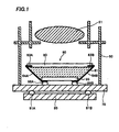
- Fig. 1 is a cross-sectional view showing a structure of a camera module according to the embodiment of this invention.
- the same symbols are assigned to the same components in Fig. 1 as in Fig.3, and explanations of them are omitted.
- CCDs which are photoelectronic transducers, are formed in a surface of a silicon chip 61 of an image sensor chip 60.
- An IR filter 90 is bonded to the silicon chip 61 with an adhesive to cover the CCDs.
- the IR filter 90 corresponds to the supporting glass substrate 62 to support the thin silicon chip 61 shown in Fig. 3, and has a filtering function in addition to a function to support the silicon chip 61.
- the IR filter 90 also serves as a supporting structure like the glass substrate 62 did in the prior art camera module.
- the IR filter 90 is obtained by vacuum deposition of metal on a glass material or incorporating copper particles into a glass material. Or, a plastic material, a surface of which has a grating structure to provide a filtering function, may be used as the IR filter 90.
- a single substrate provides both the filtering function and the chip-supporting function.
- the vacuum deposition may be made before or after bonding the glass material to the surface of the silicon chip 61.
- the IR filter 90 which blocks infrared radiation is used in an example described above. Instead, an infrared radiation pass filter, which blocks radiation other than the infrared radiation, may be used when the image sensor chip 60 is an infrared radiation image sensor chip.
- IR filter 90 Even when the function as the supporting substrate is not required, production cost can be reduced by forming the IR filter 90 on a wafer with a semiconductor wafer processing.
- various kinds of filters can be formed on a wafer, in which CCDs are formed, by forming a silicon oxide film (a kind of glass) by CVD (Chemical Vapor Deposition) or forming a SOG (Spin-On Glass) film (also a kind of glass) by coating, planarizing the silicon oxide film or the SOG film by CMP (Chemical Mechanical Polishing) and vacuum deposition of metal on the film.
- the image sensor chip 60 shown in Fig. 1 has bump electrodes 66A and 66B on its back surface.
- an image sensor chip 100 without bump electrodes as shown in Fig. 2 may be used. That is, the image sensor chip 100 has a silicon chip 101, in a surface of which CCDs are formed, IR filter 102 formed to cover the surface of the silicon chip 101 and electrode pads 103A and 103B formed on a peripheral surface of the silicon chip 101.
- the electrode pads 103A and 103B are connected to a printed circuit board through bonding wires 104A and 104B.
- the IR filter 102 is formed after the electrode pads 103A and 103B are formed by wafer processing as described above. The IR filter 102 is removed from regions on the electrode pads 103A and 103B.
Landscapes
- Engineering & Computer Science (AREA)
- Multimedia (AREA)
- Signal Processing (AREA)
- Solid State Image Pick-Up Elements (AREA)
- Studio Devices (AREA)
- Transforming Light Signals Into Electric Signals (AREA)
- Blocking Light For Cameras (AREA)
- Optical Filters (AREA)
Abstract
A camera module for mobile device is reduced in size and
production cost. CCDs, which are photoelectronic transducers,
are formed in a surface of a semiconductor chip (60)
composing an image sensor (61), and an IR filter (90) is
bonded with an adhesive to cover the surface of the semiconductor
chip (60). The IR filter (90) has a filtering
function in addition to a function to support the semiconductor
chip (60). The IR filter (90) is obtained by vacuum
deposition of metal on a glass material or incorporating
copper particles into a glass material, and implements both
filtering function and chip-supporting function.
Description
- This invention relates to a camera module, specifically to a small size camera module suitable to be incorporated into a portable device such as a mobile phone.
- A mobile phone with camera function has come into widespread use in recent years. This type of mobile phone incorporates a small size camera module. Fig. 3 is a cross-sectional view showing a structure of such a camera module.
- Fig. 3 shows a lens-
barrel 50, alens 51 mounted inside the lens-barrel 50 and anIR filter 52 attached to a mouth of the lens-barrel 50 to block infrared radiation. It also shows animage sensor chip 60 housed in a space within the lens-barrel 50 and electrically connected with a printedcircuit board 70. - The
image sensor chip 60 converts light incident from a photogenic subject through theIR filter 52 and thelens 51 into electric signals. In theimage sensor chip 60, a supportingglass substrate 62 is bonded to athin silicon chip 61, in a surface of which CCDs (Charge Coupled Devices) are formed. - Each of
redistribution wirings electrode pads image sensor chip 60, over a side surface and to a back surface of thesilicon chip 61. Each of theredistribution wirings glass substrate 65 which is bonded to the back surface of thesilicon chip 61. Each ofbump electrodes redistribution wirings glass substrate 65. Thebump electrodes circuit board 70. - A DSP (Digital Signal Processor) 80, which performs video signal processing on the electric signals from the
image sensor chip 60, is connected to a back surface of the printedcircuit board 70 throughbump electrodes - In the camera module described above, the lens-
barrel 50, thelens 51, theIR filter 52 and theimage sensor chip 60 are discrete components, and the camera module is assembled by putting these discrete components together. This causes difficulty in reducing the size and production cost of the camera module. - The object of this invention is to provide a camera module allowing for a reduced size and lower production cost.
- The solution according to the invention lies in the features of the independent claim and preferably in those of the dependent claims.
- The invention provides a camera module that comprises an image sensor chip comprising a semiconductor chip having a photoelectronic transducer formed on a surface of the semiconductor chip and a filter portion disposed on the photoelectronic transducer so as to block light incident on the filter portion at a predetermined range of wavelength, and a lens disposed above the image sensor chip.
- According to the invention the filter portion serves a dual purpose, namely to filter out unwanted radiation and to provide support for the semiconductor chip. A separate glass substrate as it is provided in the prior art camera module is no longer required. Further, a separate filter portion is no longer needed. With this invention, size and cost of the camera module are reduced.
-
- Fig. 1 is a cross-sectional view showing a camera module according to an embodiment of this invention.
- Fig. 2 is a cross-sectional view showing a camera module according to another embodiment of this invention.
- Fig. 3 is a cross-sectional view showing a conventional camera module.
-
- An embodiment of this invention will be described in detail, referring to the figures. Fig. 1 is a cross-sectional view showing a structure of a camera module according to the embodiment of this invention. The same symbols are assigned to the same components in Fig. 1 as in Fig.3, and explanations of them are omitted.
- CCDs, which are photoelectronic transducers, are formed in a surface of a
silicon chip 61 of animage sensor chip 60. AnIR filter 90 is bonded to thesilicon chip 61 with an adhesive to cover the CCDs. TheIR filter 90 corresponds to the supportingglass substrate 62 to support thethin silicon chip 61 shown in Fig. 3, and has a filtering function in addition to a function to support thesilicon chip 61. In other words, theIR filter 90 also serves as a supporting structure like theglass substrate 62 did in the prior art camera module. TheIR filter 90 is obtained by vacuum deposition of metal on a glass material or incorporating copper particles into a glass material. Or, a plastic material, a surface of which has a grating structure to provide a filtering function, may be used as theIR filter 90. A single substrate provides both the filtering function and the chip-supporting function. - When forming the
IR filter 90 by vacuum deposition of metal on the glass material, the vacuum deposition may be made before or after bonding the glass material to the surface of thesilicon chip 61. - The
IR filter 90 which blocks infrared radiation is used in an example described above. Instead, an infrared radiation pass filter, which blocks radiation other than the infrared radiation, may be used when theimage sensor chip 60 is an infrared radiation image sensor chip. - Even when the function as the supporting substrate is not required, production cost can be reduced by forming the
IR filter 90 on a wafer with a semiconductor wafer processing. For example, various kinds of filters (including IR filter 90) can be formed on a wafer, in which CCDs are formed, by forming a silicon oxide film (a kind of glass) by CVD (Chemical Vapor Deposition) or forming a SOG (Spin-On Glass) film (also a kind of glass) by coating, planarizing the silicon oxide film or the SOG film by CMP (Chemical Mechanical Polishing) and vacuum deposition of metal on the film. - The
image sensor chip 60 shown in Fig. 1 hasbump electrodes image sensor chip 100 without bump electrodes as shown in Fig. 2 may be used. That is, theimage sensor chip 100 has asilicon chip 101, in a surface of which CCDs are formed,IR filter 102 formed to cover the surface of thesilicon chip 101 andelectrode pads silicon chip 101. Theelectrode pads bonding wires IR filter 102 is formed after theelectrode pads IR filter 102 is removed from regions on theelectrode pads - With this invention, size and cost of the camera module are reduced by forming the filter material to cover the surface of the silicon chip of the image sensor chip.
Claims (7)
- A camera module comprising:an image sensor chip (60, 100) comprising a semiconductor chip (61, 101) having a photoelectronic transducer formed on a surface of the semiconductor chip and a filter portion (90, 102) disposed on the photoelectronic transducer so as to block light incident on the filter portion (90) at a predetermined range of wavelength; anda lens (51) disposed above the image sensor chip (60).
- The camera module of claim 1, wherein the filter portion (90) is configured to provide mechanical support to the semiconductor chip (60).
- The camera module of claim 1 or 2, wherein the filter portion (90) comprises a glass plate and a metal film formed on a surface of the glass plate by vapor deposition.
- The camera module of claim 1 or 2, wherein the filter portion (90) comprises a plastic plate and a grating formed on a surface of the plastic plate so as to provide a filtering function.
- The camera module of claim 1 or 2, wherein the filter portion (90) comprises a glass plate doped with copper particles or a plastic plate doped with the copper particles.
- The camera module according to any of claims 1 to 5, wherein the semiconductor chip comprises an electrode pad disposed on the surface of the semiconductor chip that does not have the photoelectronic transducer formed thereon.
- The camera module of claim 6, wherein the image sensor chip comprises a terminal (66A, B) for external connection disposed on a back surface of the image sensor chip (60) and connected to the electrode pad.
Applications Claiming Priority (2)
| Application Number | Priority Date | Filing Date | Title |
|---|---|---|---|
| JP2002366275 | 2002-12-18 | ||
| JP2002366275A JP2004200966A (en) | 2002-12-18 | 2002-12-18 | The camera module |
Publications (1)
| Publication Number | Publication Date |
|---|---|
| EP1432239A1 true EP1432239A1 (en) | 2004-06-23 |
Family
ID=32376260
Family Applications (1)
| Application Number | Title | Priority Date | Filing Date |
|---|---|---|---|
| EP03029315A Withdrawn EP1432239A1 (en) | 2002-12-18 | 2003-12-18 | Camera module |
Country Status (6)
| Country | Link |
|---|---|
| US (1) | US20040165098A1 (en) |
| EP (1) | EP1432239A1 (en) |
| JP (1) | JP2004200966A (en) |
| KR (1) | KR100543854B1 (en) |
| CN (1) | CN1509061A (en) |
| TW (1) | TWI228906B (en) |
Cited By (3)
| Publication number | Priority date | Publication date | Assignee | Title |
|---|---|---|---|---|
| EP1801849A3 (en) * | 2005-12-21 | 2008-07-02 | Sanyo Electric Co. Ltd | Semiconductor device, method of manufacturing the same, and camera module |
| CN101741972B (en) * | 2009-10-15 | 2012-08-08 | 深圳桑菲消费通信有限公司 | Dual-stroke key control system of mobile phone camera and identification method thereof |
| CN101738694B (en) * | 2008-11-04 | 2014-04-02 | 茨所株式会社 | Filter frame and camera filter unit |
Families Citing this family (19)
| Publication number | Priority date | Publication date | Assignee | Title |
|---|---|---|---|---|
| JP4563709B2 (en) * | 2004-03-29 | 2010-10-13 | 富士通株式会社 | Filter and electronic device |
| US20070001094A1 (en) * | 2005-06-29 | 2007-01-04 | Micron Technology, Inc. | Infrared filter for imagers |
| TWI386696B (en) * | 2005-10-07 | 2013-02-21 | Hon Hai Prec Ind Co Ltd | Camera module |
| JP2007188909A (en) | 2005-12-14 | 2007-07-26 | Fujifilm Corp | Solid-state imaging device and manufacturing method thereof |
| KR100772763B1 (en) * | 2006-06-29 | 2007-11-01 | 신익규 | Keypad surface pattern forming method |
| TWI383658B (en) * | 2006-08-18 | 2013-01-21 | Hon Hai Prec Ind Co Ltd | Image module |
| CN101919246A (en) * | 2007-08-08 | 2010-12-15 | 托尼·迈耶 | Non-retroreflective license plate imaging system |
| CN101498823B (en) * | 2008-01-28 | 2011-03-30 | 鸿富锦精密工业(深圳)有限公司 | Camera module group |
| JP4391585B1 (en) | 2009-06-08 | 2009-12-24 | 新光電気工業株式会社 | Camera module and manufacturing method thereof |
| US8101962B2 (en) * | 2009-10-06 | 2012-01-24 | Kuang Hong Precision Co., Ltd. | Carrying structure of semiconductor |
| KR101148847B1 (en) * | 2010-06-29 | 2012-05-29 | 주식회사 지멤스 | Image sensor module, imaging apparatus including the module and method for manufacturing the module |
| JP2014241376A (en) * | 2013-06-12 | 2014-12-25 | 住友電気工業株式会社 | Image sensor |
| US9851619B2 (en) * | 2014-10-20 | 2017-12-26 | Google Inc. | Low z-height camera module with aspherical shape blue glass |
| US10750071B2 (en) * | 2016-03-12 | 2020-08-18 | Ningbo Sunny Opotech Co., Ltd. | Camera module with lens array arrangement, circuit board assembly, and image sensor and manufacturing method thereof |
| US10325952B2 (en) * | 2017-07-07 | 2019-06-18 | Advanced Semiconductor Engineering, Inc. | Semiconductor package device and method of manufacturing the same |
| JP6267823B1 (en) * | 2017-07-27 | 2018-01-24 | 日本板硝子株式会社 | Optical filter, camera module, and information terminal |
| JP6232161B1 (en) | 2017-07-27 | 2017-11-15 | 日本板硝子株式会社 | Optical filter |
| CN113795559B (en) | 2019-05-23 | 2022-08-30 | 日本板硝子株式会社 | Light absorbing composition, light absorbing film, and optical filter |
| US11276724B2 (en) * | 2019-06-27 | 2022-03-15 | Semiconductor Components Industries, Llc | Electrical interconnection of image sensor package |
Citations (8)
| Publication number | Priority date | Publication date | Assignee | Title |
|---|---|---|---|---|
| JPS6178160A (en) * | 1984-09-25 | 1986-04-21 | Matsushita Electric Ind Co Ltd | Color solid-state imaging device |
| US4745470A (en) * | 1986-04-04 | 1988-05-17 | Olympus Optical Co., Ltd. | Endoscope using a chip carrier type solid state imaging device |
| US5283691A (en) * | 1991-02-15 | 1994-02-01 | Olympus Optical Co., Ltd. | Solid state imaging apparatus |
| WO1999040624A1 (en) * | 1998-02-06 | 1999-08-12 | Shellcase Ltd. | Integrated circuit device |
| US6342460B1 (en) * | 1998-06-22 | 2002-01-29 | Olympus Optical Co., Ltd. | Infrared absorbing glass, and it's fabrication method |
| WO2002014949A1 (en) * | 2000-08-11 | 2002-02-21 | Em Microelectronic-Marin Sa | Small-size imaging apparatus, in particular photographic appliance or camera |
| US20020171031A1 (en) * | 2001-05-16 | 2002-11-21 | Samsung Electro-Mechanics Co., Ltd. | Image sensor module and method for fabricating the same |
| US20030164891A1 (en) * | 2002-02-21 | 2003-09-04 | Kazuo Akimoto | Solidstate image-taking apparatus and laminated chip for use therewith |
Family Cites Families (5)
| Publication number | Priority date | Publication date | Assignee | Title |
|---|---|---|---|---|
| US6217796B1 (en) * | 1998-11-17 | 2001-04-17 | Nisshinbo Industries, Inc. | Near infrared absorption composition |
| US6559439B1 (en) * | 1999-12-15 | 2003-05-06 | Olympus Optical Co., Ltd. | Image taking lens unit with frame member for positioning lens and substrate |
| JP3762618B2 (en) * | 2000-06-19 | 2006-04-05 | ペンタックス株式会社 | Electronic camera |
| JP2002156607A (en) * | 2000-11-16 | 2002-05-31 | Victor Co Of Japan Ltd | Imaging device |
| JP2002231918A (en) * | 2001-02-06 | 2002-08-16 | Olympus Optical Co Ltd | Solid-state imaging device and manufacturing method thereof |
-
2002
- 2002-12-18 JP JP2002366275A patent/JP2004200966A/en not_active Withdrawn
-
2003
- 2003-12-08 TW TW092134528A patent/TWI228906B/en not_active IP Right Cessation
- 2003-12-17 KR KR1020030092236A patent/KR100543854B1/en not_active Expired - Fee Related
- 2003-12-17 US US10/736,906 patent/US20040165098A1/en not_active Abandoned
- 2003-12-18 CN CNA2003101206709A patent/CN1509061A/en active Pending
- 2003-12-18 EP EP03029315A patent/EP1432239A1/en not_active Withdrawn
Patent Citations (8)
| Publication number | Priority date | Publication date | Assignee | Title |
|---|---|---|---|---|
| JPS6178160A (en) * | 1984-09-25 | 1986-04-21 | Matsushita Electric Ind Co Ltd | Color solid-state imaging device |
| US4745470A (en) * | 1986-04-04 | 1988-05-17 | Olympus Optical Co., Ltd. | Endoscope using a chip carrier type solid state imaging device |
| US5283691A (en) * | 1991-02-15 | 1994-02-01 | Olympus Optical Co., Ltd. | Solid state imaging apparatus |
| WO1999040624A1 (en) * | 1998-02-06 | 1999-08-12 | Shellcase Ltd. | Integrated circuit device |
| US6342460B1 (en) * | 1998-06-22 | 2002-01-29 | Olympus Optical Co., Ltd. | Infrared absorbing glass, and it's fabrication method |
| WO2002014949A1 (en) * | 2000-08-11 | 2002-02-21 | Em Microelectronic-Marin Sa | Small-size imaging apparatus, in particular photographic appliance or camera |
| US20020171031A1 (en) * | 2001-05-16 | 2002-11-21 | Samsung Electro-Mechanics Co., Ltd. | Image sensor module and method for fabricating the same |
| US20030164891A1 (en) * | 2002-02-21 | 2003-09-04 | Kazuo Akimoto | Solidstate image-taking apparatus and laminated chip for use therewith |
Non-Patent Citations (1)
| Title |
|---|
| PATENT ABSTRACTS OF JAPAN vol. 010, no. 248 (E - 431) 26 August 1986 (1986-08-26) * |
Cited By (4)
| Publication number | Priority date | Publication date | Assignee | Title |
|---|---|---|---|---|
| EP1801849A3 (en) * | 2005-12-21 | 2008-07-02 | Sanyo Electric Co. Ltd | Semiconductor device, method of manufacturing the same, and camera module |
| US7576402B2 (en) | 2005-12-21 | 2009-08-18 | Sanyo Electric Co., Ltd. | Semiconductor device, method of manufacturing the same, and camera module |
| CN101738694B (en) * | 2008-11-04 | 2014-04-02 | 茨所株式会社 | Filter frame and camera filter unit |
| CN101741972B (en) * | 2009-10-15 | 2012-08-08 | 深圳桑菲消费通信有限公司 | Dual-stroke key control system of mobile phone camera and identification method thereof |
Also Published As
| Publication number | Publication date |
|---|---|
| KR20040054523A (en) | 2004-06-25 |
| TW200418309A (en) | 2004-09-16 |
| US20040165098A1 (en) | 2004-08-26 |
| JP2004200966A (en) | 2004-07-15 |
| CN1509061A (en) | 2004-06-30 |
| KR100543854B1 (en) | 2006-01-23 |
| TWI228906B (en) | 2005-03-01 |
Similar Documents
| Publication | Publication Date | Title |
|---|---|---|
| US20040165098A1 (en) | Camera module | |
| KR100608420B1 (en) | Image sensor chip package and manufacturing method thereof | |
| US7948555B2 (en) | Camera module and electronic apparatus having the same | |
| US6853005B2 (en) | Camera module and manufacturing method thereof | |
| US7414663B2 (en) | Imaging element, imaging device, camera module and camera system | |
| US7923798B2 (en) | Optical device and method for fabricating the same, camera module using optical device, and electronic equipment mounting camera module | |
| US6737292B2 (en) | Method of fabricating an image sensor module at the wafer level and mounting on circuit board | |
| EP1434426A2 (en) | Camera module and manufacturing method thereof | |
| CN101652695B (en) | Wafer level camera module and method of manufacture | |
| JP2003198897A (en) | Optical module, circuit board and electronic equipment | |
| KR20060049586A (en) | Solid-state imaging device, method for manufacturing same, and camera module | |
| US7605404B2 (en) | Image pickup device and method of manufacturing the same | |
| JP3867785B2 (en) | Optical module | |
| US20030146998A1 (en) | Small-size imaging apparatus, in particular photographic appliance or camera | |
| JP4720120B2 (en) | Semiconductor image sensor module | |
| CN100459134C (en) | solid state imaging device | |
| CN101536489B (en) | Solid-state imaging device and electronic equipment | |
| US20090315130A1 (en) | Solid-state imaging apparatus and method for manufacturing the same | |
| JP3674777B2 (en) | Solid-state imaging device | |
| JP3017780B2 (en) | Electronic endoscope imaging device | |
| JP4138436B2 (en) | Optical module, circuit board and electronic device | |
| KR100640336B1 (en) | Image sensor assembly | |
| EP1713126A1 (en) | Image pickup device and a manufacturing method thereof | |
| JP2009111130A (en) | Imaging apparatus and manufacturing method thereof | |
| JP2011077555A (en) | Semiconductor image sensor module, and method of manufacturing semiconductor image sensor module |
Legal Events
| Date | Code | Title | Description |
|---|---|---|---|
| PUAI | Public reference made under article 153(3) epc to a published international application that has entered the european phase |
Free format text: ORIGINAL CODE: 0009012 |
|
| AK | Designated contracting states |
Kind code of ref document: A1 Designated state(s): AT BE BG CH CY CZ DE DK EE ES FI FR GB GR HU IE IT LI LU MC NL PT RO SE SI SK TR |
|
| AX | Request for extension of the european patent |
Extension state: AL LT LV MK |
|
| 17P | Request for examination filed |
Effective date: 20041222 |
|
| AKX | Designation fees paid |
Designated state(s): DE FI FR GB |
|
| 17Q | First examination report despatched |
Effective date: 20071030 |
|
| STAA | Information on the status of an ep patent application or granted ep patent |
Free format text: STATUS: THE APPLICATION IS DEEMED TO BE WITHDRAWN |
|
| 18D | Application deemed to be withdrawn |
Effective date: 20080311 |