EP1432042A2 - Thin film transistor with LDD/offset structure - Google Patents
Thin film transistor with LDD/offset structure Download PDFInfo
- Publication number
- EP1432042A2 EP1432042A2 EP03090437A EP03090437A EP1432042A2 EP 1432042 A2 EP1432042 A2 EP 1432042A2 EP 03090437 A EP03090437 A EP 03090437A EP 03090437 A EP03090437 A EP 03090437A EP 1432042 A2 EP1432042 A2 EP 1432042A2
- Authority
- EP
- European Patent Office
- Prior art keywords
- thin film
- film transistor
- crystal grain
- grain boundaries
- ldd
- Prior art date
- Legal status (The legal status is an assumption and is not a legal conclusion. Google has not performed a legal analysis and makes no representation as to the accuracy of the status listed.)
- Ceased
Links
Images



Classifications
-
- H—ELECTRICITY
- H10—SEMICONDUCTOR DEVICES; ELECTRIC SOLID-STATE DEVICES NOT OTHERWISE PROVIDED FOR
- H10D—INORGANIC ELECTRIC SEMICONDUCTOR DEVICES
- H10D30/00—Field-effect transistors [FET]
- H10D30/60—Insulated-gate field-effect transistors [IGFET]
- H10D30/67—Thin-film transistors [TFT]
-
- H—ELECTRICITY
- H10—SEMICONDUCTOR DEVICES; ELECTRIC SOLID-STATE DEVICES NOT OTHERWISE PROVIDED FOR
- H10D—INORGANIC ELECTRIC SEMICONDUCTOR DEVICES
- H10D30/00—Field-effect transistors [FET]
- H10D30/01—Manufacture or treatment
- H10D30/021—Manufacture or treatment of FETs having insulated gates [IGFET]
- H10D30/031—Manufacture or treatment of FETs having insulated gates [IGFET] of thin-film transistors [TFT]
- H10D30/0312—Manufacture or treatment of FETs having insulated gates [IGFET] of thin-film transistors [TFT] characterised by the gate electrodes
- H10D30/0314—Manufacture or treatment of FETs having insulated gates [IGFET] of thin-film transistors [TFT] characterised by the gate electrodes of lateral top-gate TFTs comprising only a single gate
-
- H—ELECTRICITY
- H10—SEMICONDUCTOR DEVICES; ELECTRIC SOLID-STATE DEVICES NOT OTHERWISE PROVIDED FOR
- H10D—INORGANIC ELECTRIC SEMICONDUCTOR DEVICES
- H10D30/00—Field-effect transistors [FET]
- H10D30/01—Manufacture or treatment
- H10D30/021—Manufacture or treatment of FETs having insulated gates [IGFET]
- H10D30/031—Manufacture or treatment of FETs having insulated gates [IGFET] of thin-film transistors [TFT]
- H10D30/0321—Manufacture or treatment of FETs having insulated gates [IGFET] of thin-film transistors [TFT] comprising silicon, e.g. amorphous silicon or polysilicon
-
- H—ELECTRICITY
- H10—SEMICONDUCTOR DEVICES; ELECTRIC SOLID-STATE DEVICES NOT OTHERWISE PROVIDED FOR
- H10D—INORGANIC ELECTRIC SEMICONDUCTOR DEVICES
- H10D30/00—Field-effect transistors [FET]
- H10D30/60—Insulated-gate field-effect transistors [IGFET]
- H10D30/67—Thin-film transistors [TFT]
- H10D30/6704—Thin-film transistors [TFT] having supplementary regions or layers in the thin films or in the insulated bulk substrates for controlling properties of the device
- H10D30/6713—Thin-film transistors [TFT] having supplementary regions or layers in the thin films or in the insulated bulk substrates for controlling properties of the device characterised by the properties of the source or drain regions, e.g. compositions or sectional shapes
- H10D30/6715—Thin-film transistors [TFT] having supplementary regions or layers in the thin films or in the insulated bulk substrates for controlling properties of the device characterised by the properties of the source or drain regions, e.g. compositions or sectional shapes characterised by the doping profiles, e.g. having lightly-doped source or drain extensions
-
- H—ELECTRICITY
- H10—SEMICONDUCTOR DEVICES; ELECTRIC SOLID-STATE DEVICES NOT OTHERWISE PROVIDED FOR
- H10D—INORGANIC ELECTRIC SEMICONDUCTOR DEVICES
- H10D30/00—Field-effect transistors [FET]
- H10D30/60—Insulated-gate field-effect transistors [IGFET]
- H10D30/67—Thin-film transistors [TFT]
- H10D30/6729—Thin-film transistors [TFT] characterised by the electrodes
- H10D30/673—Thin-film transistors [TFT] characterised by the electrodes characterised by the shapes, relative sizes or dispositions of the gate electrodes
- H10D30/6731—Top-gate only TFTs
-
- H—ELECTRICITY
- H10—SEMICONDUCTOR DEVICES; ELECTRIC SOLID-STATE DEVICES NOT OTHERWISE PROVIDED FOR
- H10D—INORGANIC ELECTRIC SEMICONDUCTOR DEVICES
- H10D30/00—Field-effect transistors [FET]
- H10D30/60—Insulated-gate field-effect transistors [IGFET]
- H10D30/67—Thin-film transistors [TFT]
- H10D30/674—Thin-film transistors [TFT] characterised by the active materials
- H10D30/6741—Group IV materials, e.g. germanium or silicon carbide
- H10D30/6743—Silicon
- H10D30/6745—Polycrystalline or microcrystalline silicon
-
- H—ELECTRICITY
- H10—SEMICONDUCTOR DEVICES; ELECTRIC SOLID-STATE DEVICES NOT OTHERWISE PROVIDED FOR
- H10D—INORGANIC ELECTRIC SEMICONDUCTOR DEVICES
- H10D30/00—Field-effect transistors [FET]
- H10D30/60—Insulated-gate field-effect transistors [IGFET]
- H10D30/67—Thin-film transistors [TFT]
- H10D30/6757—Thin-film transistors [TFT] characterised by the structure of the channel, e.g. transverse or longitudinal shape or doping profile
-
- H—ELECTRICITY
- H10—SEMICONDUCTOR DEVICES; ELECTRIC SOLID-STATE DEVICES NOT OTHERWISE PROVIDED FOR
- H10D—INORGANIC ELECTRIC SEMICONDUCTOR DEVICES
- H10D62/00—Semiconductor bodies, or regions thereof, of devices having potential barriers
- H10D62/40—Crystalline structures
-
- H—ELECTRICITY
- H10—SEMICONDUCTOR DEVICES; ELECTRIC SOLID-STATE DEVICES NOT OTHERWISE PROVIDED FOR
- H10D—INORGANIC ELECTRIC SEMICONDUCTOR DEVICES
- H10D86/00—Integrated devices formed in or on insulating or conducting substrates, e.g. formed in silicon-on-insulator [SOI] substrates or on stainless steel or glass substrates
- H10D86/01—Manufacture or treatment
- H10D86/021—Manufacture or treatment of multiple TFTs
- H10D86/0251—Manufacture or treatment of multiple TFTs characterised by increasing the uniformity of device parameters
Definitions
- the present invention relates to a thin film transistor with an LDD region, and, more particularly, to a thin film transistor with an LDD region in which the electrical characteristics, such as the current characteristics, are superior.
- TFT thin film transistor
- the size, size uniformity, number, position, and direction of crystal grains not only have a fatal effect upon TFT characteristics such as threshold voltage (Vth), subthreshold slope, charge carrier mobility, leakage current, and device stability, directly and indirectly, but they also have a fatal effect upon the uniformity of the TFTs, depending on the position of the crystal grains during fabrication of an active matrix display substrate using TFTs.
- Vth threshold voltage
- subthreshold slope charge carrier mobility
- leakage current leakage current
- device stability directly and indirectly, but they also have a fatal effect upon the uniformity of the TFTs, depending on the position of the crystal grains during fabrication of an active matrix display substrate using TFTs.
- the number of fatal crystal grain boundaries (hereinafter referred to as "primary" crystal grain boundaries) included in active channel regions of TFTs on the whole substrate of a display device can be equivalent or changed according to the size of the crystal grains, inclination angle ⁇ , dimension of active channels (length (L), width (W)), and position of each TFT on the substrate (FIG 1A and FIG. 1B).
- the maximum number of crystal grain boundaries is Nmax in the number of "primary" crystal grain boundaries included in the active channel regions for the size of crystal grains Gs, active channel dimension L X W, and inclination angle ⁇
- the number of "primary" crystal grain boundaries included in the active channel regions, according to the position of the TFT on a substrate or display device will be Nmax (3 in case of FIG. 1B) or Nmax-1 (2 in case of FIG. 1A), and uniformity of the most excellent TFT characteristics can be secured when Nmax "primary" crystal grain boundaries are included in active channel regions for all TFTs. That is, the more equal the number of crystal grain boundaries each TFT has, the more excellent uniformity a device obtains.
- polycrystalline or single crystalline particles are capable of forming large silicon grains on a substrate using a sequential lateral solidification (SLS) crystallization method, and it is reported that characteristics similar to the characteristics of TFTs fabricated of single crystalline silicon are obtained when fabricating a TFT using the large silicon grains.
- SLS sequential lateral solidification
- TFTs for driver and pixel arrays must be fabricated to fabricate an active matrix display.
- TFT liquid crystal display
- organic luminescent substance for example, organic electroluminescent device
- TFTs by growing a certain number of crystal grains, in a certain direction only, for the active channel regions of each of one million to two million, or more, TFTs.
- the selected region is also a considerably large region compared to an active channel region having a dimension of several ⁇ m x several ⁇ m.
- the size of the laser beam used in the SLS crystallization method is approximately several mm x dozens of mm, and the stepping and shifting of the laser beam or stage are essentially required to crystallize amorphous silicon of the whole region or selected region on a substrate, wherein misalignment between regions on which the laser beam is irradiated exists. Therefore, the number of "primary" crystal grain boundaries included in the numerous active channel regions of TFTs varies, and TFTs on the whole substrate, or in the driver region and pixel cell region, have unpredictable nonuniformity. The nonuniformity has a fatal adverse effect on the embodiment of an active matrix display device.
- TFTs in driver circuits are generally inclined to TFTs in pixel cell regions at an angle of 90° when fabricating an active matrix display, wherein the uniformity of the device can be improved by fabricating TFTs in such a way that the direction of the active channel regions is inclined to the crystal grain growing direction in an angle of 30 to 60° to improve uniformity of characteristics between TFTs, as characteristics of each TFT are not greatly deteriorated, as illustrated in FIG. 3C.
- the present invention is suggested to solve the foregoing and/or otherproblems, and it is an aspect of the present invention to provide an organic electroluminescent device with an LDD/offset region in which "primary" crystal grain boundaries of polysilicon are not included in a lightly doped drain (LDD)/offset region to improve electrical characteristics such as current characteristics.
- LDD lightly doped drain
- the present invention provides a thin film transistor comprising an LDD region or offset region, wherein the thin film transistor is formed so that "primary" crystal grain boundaries of a poly silicon substrate are not positioned in the LDD or offset region.
- the present invention provides a flat panel display device comprising a thin film transistor comprising an LDD region or offset region, wherein the thin film transistor is formed so that "primary" crystal grain boundaries of a poly silicon substrate are not positioned in the LDD or offset region.
- Crystal grain boundaries are formed between adjacent crystal grains due to a limited size of crystal grains if crystal grains of polycrystalline silicon having an important effect on TFT characteristics, directly and indirectly, during fabrication of TFT for active matrix displays are large and regularized for improvement of the TFT characteristics.
- crystal grain size means the confirmable distance between crystal grain boundaries, and is generally defined as the distance between crystal grain boundaries belonging to the ordinary error range.
- Crystal grain boundaries have a fatal effect on TFT characteristics when crystal grain boundaries exist in active channel regions.
- "Primary" crystal grain boundaries in which an inclination angle of the crystal grain boundaries to a direction perpendicular to an active channel direction is -45° ⁇ ⁇ 45°,become an inevitable defect due to the limitation of process accuracy when forming a polycrystalline silicon thin film.
- the number of "primary" crystal grain boundaries included in active channel regions of a TFT fabricated on a driver circuit substrate or display substrate can be varied depending on the size and direction of the crystal grains and the dimensions of the active channels as illustrated in FIG. 4. Therefore, TFTs and displays that are fabricated have nonuniform characteristics, and can not be evenly driven.
- TFT characteristics are affected by the "primary" crystal grain boundaries when the "primary" crystal grain boundaries exist in the LDD region in TFTs having an LDD structure stated in an embodiment of the present invention.
- an offset region refers to a region that is not doped between the source electrode and the drain electrode, and leakage current can be cutoff by interposition of the offset region. Furthermore, off current, that is, leakage current, can be reduced in a thin film transistor by adding an LDD region to the offset region through low density ion doping of impurities.
- FIG. 5 is a cross sectional view of a thin film transistor having an offset region or LDD structure.
- a thin film transistor with an offset region or LDD structure comprises a buffer layer 12, activation layer 13, and gate insulation film 14 which are sequentially formed on a substrate 11; a conductive gate electrode 15 which is formed on the buffer layer 12, activation layer 13 and gate insulation film 14; a passivation layer 16 that is formed over the surface of the gate insulation film 14; contact holes which are formed on the gate insulation film 14 and the passivation layer 16; a conductive layer which is formed over the surface of the passivation layer 16; and drain and source electrodes 17 which are formed by patterning the conductive layer.
- drain and source regions 13a are formed on the activation layer 13, a channel region I is formed in the activation layer 13 of the lower part of the gate electrode 15, and an LDD region II, doped with low concentrated impurities, is formed between the drain region 13a and the channel region, and between the source region 13a and the channel region.
- the activation layer 13 is formed by crystallizing amorphous silicon, thereby patterning polycrystalline silicon, crystal grain boundaries are formed in the polycrystalline silicon as described above, and, particularly, the "primary" crystal grain boundaries are deeply associated with the electrical characteristics of the TFT. That is, they greatly influence the driving current, as the "primary" crystal grain boundaries function as a barrier of current flowing from source to drain.
- "primary" crystal grain boundaries of polysilicon forming the activation layer 13 are not positioned in the LDD region II, formed to prevent leakage current, so that characteristics of leakage current are improved.
- FIG. 6 is a plan figure schematically illustrating a thin film transistor having an offset region, or LDD structure.
- a thin film transistor can be formed by adjusting the width between the "primary" crystal grain boundaries formed on polysilicon so that the "primary" crystal grain boundaries are not formed on the LDD region II.
- an activation layer 13 can be formed so that the "primary" crystal grain boundaries are not included in the LDD region II.
- the width between "primary" crystal grain boundaries of polysilicon forming the activation layer 13 should be wider than that of the LDD region II.
- a thin film transistor according to an embodiment of the present invention has improved device characteristics, and it has superior electrical characteristics, such as leakage current characteristics.
- a semiconductor device or display device can be used as the device, and a liquid crystal device (LCD) or organic electroluminescent (EL) device is preferably used as a display device.
- LCD liquid crystal device
- EL organic electroluminescent
- the polysilicon forming the activation layer is formed by the SLS method.
- a thin film transistor according to an embodiment of the present invention is capable of providing TFTs with superior electrical characteristics and improved reliability.
Landscapes
- Thin Film Transistor (AREA)
- Recrystallisation Techniques (AREA)
- Liquid Crystal (AREA)
- Electroluminescent Light Sources (AREA)
Abstract
Description
- This application claims the priority of Korean Patent Application No. 2002-80326, filed December 16, 2002, in the Korean Intellectual Property Office, the disclosure of which is incorporated herein by reference.
- The present invention relates to a thin film transistor with an LDD region, and, more particularly, to a thin film transistor with an LDD region in which the electrical characteristics, such as the current characteristics, are superior.
- During fabrication of a thin film transistor (TFT) using polycrystalline silicon, bonding defects, such as dangling bonds, existing on crystal grain boundaries of the polycrystalline silicon included in an active channel region are known to act as a trap for electric charge carriers.
- Therefore, the size, size uniformity, number, position, and direction of crystal grains not only have a fatal effect upon TFT characteristics such as threshold voltage (Vth), subthreshold slope, charge carrier mobility, leakage current, and device stability, directly and indirectly, but they also have a fatal effect upon the uniformity of the TFTs, depending on the position of the crystal grains during fabrication of an active matrix display substrate using TFTs.
- The number of fatal crystal grain boundaries (hereinafter referred to as "primary" crystal grain boundaries) included in active channel regions of TFTs on the whole substrate of a display device can be equivalent or changed according to the size of the crystal grains, inclination angle ⊖, dimension of active channels (length (L), width (W)), and position of each TFT on the substrate (FIG 1A and FIG. 1B).
- As illustrated in FIG. 1A and FIG. 1B, if the maximum number of crystal grain boundaries is Nmax in the number of "primary" crystal grain boundaries included in the active channel regions for the size of crystal grains Gs, active channel dimension L X W, and inclination angle Θ, the number of "primary" crystal grain boundaries included in the active channel regions, according to the position of the TFT on a substrate or display device will be Nmax (3 in case of FIG. 1B) or Nmax-1 (2 in case of FIG. 1A), and uniformity of the most excellent TFT characteristics can be secured when Nmax "primary" crystal grain boundaries are included in active channel regions for all TFTs. That is, the more equal the number of crystal grain boundaries each TFT has, the more excellent uniformity a device obtains.
- On the other hand, if the number of TFTs including Nmax "primary" crystal grain boundaries is equivalent to the number of TFTs including Nmax-1 "primary" crystal grain boundaries, it can be easily expected that uniformity is the worst, resulting in undesirable characteristics of TFTs on a TFT substrate or a display device.
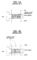
- As illustrated in FIG. 2A and FIG. 2B, polycrystalline or single crystalline particles are capable of forming large silicon grains on a substrate using a sequential lateral solidification (SLS) crystallization method, and it is reported that characteristics similar to the characteristics of TFTs fabricated of single crystalline silicon are obtained when fabricating a TFT using the large silicon grains.
- However, numerous TFTs for driver and pixel arrays must be fabricated to fabricate an active matrix display.
- For example, approximately one million pixels are made in fabricating an active matrix display having SVGA resolution, and one TFT is required in each pixel in the case of a liquid crystal display (LCD), and at least two or more TFTs are required in a display using an organic luminescent substance (for example, organic electroluminescent device).
- Therefore, it is impossible to fabricate TFTs by growing a certain number of crystal grains, in a certain direction only, for the active channel regions of each of one million to two million, or more, TFTs.
- As a method to realize this, technology for transforming amorphous silicon on the whole substrate into polycrystalline silicon, or crystallizing the selected region only on the substrate by the SLS crystallization method after depositing amorphous silicon by PECVD, LPCV, or sputtering, is disclosed, referring to FIG. 2A and FIG. 2B, as disclosed in PCT international patent WO 97/45827.
- The selected region is also a considerably large region compared to an active channel region having a dimension of several µm x several µm. Furthermore, the size of the laser beam used in the SLS crystallization method is approximately several mm x dozens of mm, and the stepping and shifting of the laser beam or stage are essentially required to crystallize amorphous silicon of the whole region or selected region on a substrate, wherein misalignment between regions on which the laser beam is irradiated exists. Therefore, the number of "primary" crystal grain boundaries included in the numerous active channel regions of TFTs varies, and TFTs on the whole substrate, or in the driver region and pixel cell region, have unpredictable nonuniformity. The nonuniformity has a fatal adverse effect on the embodiment of an active matrix display device.
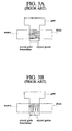
- Furthermore, it is disclosed in US Patent No. 6,177,391 that a barrier effect of crystal grain boundaries in the direction of the electric charge carrier is minimized, in the case that the direction of the active channels is parallel to the direction of grown crystal grains by the SLS crystallization method when fabricating a TFT for LCD devices, including a driver and pixel array, by forming large silicon grains using the SLS crystallization method as illustrated in FIG. 3A. Therefore, TFT characteristics second to single crystalline silicon can be obtained. On the other hand, crystal grain boundaries in which TFT characteristics act as a trap of the electric charge carrier exist, and TFT characteristics are greatly deteriorated, in the case that the direction of the active channels is perpendicular to the growing direction of the crystal grains, as illustrated in FIG. 3B.
- Actually, there are cases in which TFTs in driver circuits are generally inclined to TFTs in pixel cell regions at an angle of 90° when fabricating an active matrix display, wherein the uniformity of the device can be improved by fabricating TFTs in such a way that the direction of the active channel regions is inclined to the crystal grain growing direction in an angle of 30 to 60° to improve uniformity of characteristics between TFTs, as characteristics of each TFT are not greatly deteriorated, as illustrated in FIG. 3C.
- However, there is a probability that fatal crystal grain boundaries are included in the active channel regions since this method also uses crystal grains having a limited size formed by the SLS crystallization method. Therefore, this method has problems in that unpredictable nonuniformity exists, causing differences of characteristics between TFTs.
- The present invention is suggested to solve the foregoing and/or otherproblems, and it is an aspect of the present invention to provide an organic electroluminescent device with an LDD/offset region in which "primary" crystal grain boundaries of polysilicon are not included in a lightly doped drain (LDD)/offset region to improve electrical characteristics such as current characteristics.
- Additional objects and advantages of the invention will be set forth in part in the description which follows and, in part, will be obvious from the description, or may be learned by practice of the invention.
- In order to achieve the foregoing and/or other aspects, the present invention provides a thin film transistor comprising an LDD region or offset region, wherein the thin film transistor is formed so that "primary" crystal grain boundaries of a poly silicon substrate are not positioned in the LDD or offset region.
- Also, the present invention provides a flat panel display device comprising a thin film transistor comprising an LDD region or offset region, wherein the thin film transistor is formed so that "primary" crystal grain boundaries of a poly silicon substrate are not positioned in the LDD or offset region.
- These and/or other aspects and advantages of the invention will become apparent and more readily appreciated from the following description of the preferred embodiments, taken in conjunction with the accompanying drawings of which:
- FIG.1A is a plan figure schematically illustrating a TFT in which the number of fatal crystal grain boundaries for the size of equal crystal grains Gs, and the dimension of active channels L x W, is 2;
- FIG. 1B is a plan figure schematically illustrating a TFT in which the number of fatal crystal grain boundaries is 3;
- FIG. 2A and FIG. 2B are plan figures schematically illustrating active channels of TFTs including silicon grains having a large grain size formed by the SLS crystallization method;
- FIG. 3A to FIG. 3C are plan figures schematically illustrating active channels of TFTs fabricated according to other related art;
- FIG. 4 is a schematic drawing indicating that the number of fatal crystal grain boundaries capable of having a fatal effect on the characteristics of a TFT fabricated on a driver circuit substrate or display can be varied depending on the position of the TFT;
- FIG. 5 is a cross sectional view of a thin film transistor having an offset or LDD structure; and
- FIG. 6 is a plan figure schematically illustrating a thin film transistor having an offset or LDD structure.
-
- Reference will now be made in detail to the present preferred embodiments of the present invention, examples of which are illustrated in the accompanying drawings, wherein like reference numerals refer to the like elements throughout. The embodiments are described below in order to explain the present invention by referring to the figures.
- Crystal grain boundaries are formed between adjacent crystal grains due to a limited size of crystal grains if crystal grains of polycrystalline silicon having an important effect on TFT characteristics, directly and indirectly, during fabrication of TFT for active matrix displays are large and regularized for improvement of the TFT characteristics.
- In the present invention, "crystal grain size" means the confirmable distance between crystal grain boundaries, and is generally defined as the distance between crystal grain boundaries belonging to the ordinary error range.
- Particularly, crystal grain boundaries have a fatal effect on TFT characteristics when crystal grain boundaries exist in active channel regions. "Primary" crystal grain boundaries, in which an inclination angle of the crystal grain boundaries to a direction perpendicular to an active channel direction is -45°≤ ⊖≤ 45°,become an inevitable defect due to the limitation of process accuracy when forming a polycrystalline silicon thin film.
- Furthermore, the number of "primary" crystal grain boundaries included in active channel regions of a TFT fabricated on a driver circuit substrate or display substrate can be varied depending on the size and direction of the crystal grains and the dimensions of the active channels as illustrated in FIG. 4. Therefore, TFTs and displays that are fabricated have nonuniform characteristics, and can not be evenly driven.
- TFT characteristics are affected by the "primary" crystal grain boundaries when the "primary" crystal grain boundaries exist in the LDD region in TFTs having an LDD structure stated in an embodiment of the present invention.
- Generally, an offset region refers to a region that is not doped between the source electrode and the drain electrode, and leakage current can be cutoff by interposition of the offset region. Furthermore, off current, that is, leakage current, can be reduced in a thin film transistor by adding an LDD region to the offset region through low density ion doping of impurities.
- FIG. 5 is a cross sectional view of a thin film transistor having an offset region or LDD structure.
- Referring to FIG. 5, a thin film transistor with an offset region or LDD structure comprises a
buffer layer 12,activation layer 13, andgate insulation film 14 which are sequentially formed on asubstrate 11; aconductive gate electrode 15 which is formed on thebuffer layer 12,activation layer 13 andgate insulation film 14; apassivation layer 16 that is formed over the surface of thegate insulation film 14; contact holes which are formed on thegate insulation film 14 and thepassivation layer 16; a conductive layer which is formed over the surface of thepassivation layer 16; and drain andsource electrodes 17 which are formed by patterning the conductive layer. - Furthermore, drain and
source regions 13a, doped with high concentrated impurities, are formed on theactivation layer 13, a channel region I is formed in theactivation layer 13 of the lower part of thegate electrode 15, and an LDD region II, doped with low concentrated impurities, is formed between thedrain region 13a and the channel region, and between thesource region 13a and the channel region. - Generally, when the
activation layer 13 is formed by crystallizing amorphous silicon, thereby patterning polycrystalline silicon, crystal grain boundaries are formed in the polycrystalline silicon as described above, and, particularly, the "primary" crystal grain boundaries are deeply associated with the electrical characteristics of the TFT. That is, they greatly influence the driving current, as the "primary" crystal grain boundaries function as a barrier of current flowing from source to drain. - In an embodiment of the present invention, "primary" crystal grain boundaries of polysilicon forming the
activation layer 13 are not positioned in the LDD region II, formed to prevent leakage current, so that characteristics of leakage current are improved. - FIG. 6 is a plan figure schematically illustrating a thin film transistor having an offset region, or LDD structure.
- Referring to FIG. 6, a thin film transistor can be formed by adjusting the width between the "primary" crystal grain boundaries formed on polysilicon so that the "primary" crystal grain boundaries are not formed on the LDD region II.
- Furthermore, an
activation layer 13 can be formed so that the "primary" crystal grain boundaries are not included in the LDD region II. In this case, the width between "primary" crystal grain boundaries of polysilicon forming theactivation layer 13 should be wider than that of the LDD region II. - Therefore, a thin film transistor according to an embodiment of the present invention has improved device characteristics, and it has superior electrical characteristics, such as leakage current characteristics. A semiconductor device or display device can be used as the device, and a liquid crystal device (LCD) or organic electroluminescent (EL) device is preferably used as a display device.
- It is preferable that the polysilicon forming the activation layer is formed by the SLS method.
- A thin film transistor according to an embodiment of the present invention is capable of providing TFTs with superior electrical characteristics and improved reliability.
- Although a few embodiments of the present invention have been shown and described, it would be appreciated by those skilled in the art that changes may be made in these embodiments without departing from the principles and spirit of the invention, the scope of which is define in the claims and their equivalents.
Claims (12)
- A thin film transistor (TFT) comprising a lightly doped drain (LDD) region or offset region, wherein the thin film transistor is formed so that primary crystal grain boundaries of a polysilicon substrate are not positioned in the LDD or offset region.
- The thin film transistor according to claim 1, wherein a width of an activation layer including the LDD region or offset region is shorter than a distance between the primary crystal grain boundaries.
- The thin film transistor according to claim 1, wherein the polysilicon substrate is formed by a sequential lateral solidification (SLS) method.
- The thin film transistor according to claim 1, wherein the thin film transistor is used in an LCD (liquid crystal display) or organic EL (electroluminescent) device.
- The thin film transistor according to claim 1, wherein the primary crystal grain boundaries are perpendicular to a current direction between active channel regions of the thin film transistor.
- The thin film transistor according to claim 1, wherein the primary crystal grain boundaries are inclined to a current direction between active channel regions of the thin film transistor at an angle of -45° ≤ Θ ≤ 45°.
- A flat panel display device comprising:wherein the thin film transistor is formed so that primary crystal grain boundaries of a polysilicon substrate are not positioned in the LDD or offset region.a thin film transistor comprising:an LDD region or offset region,
- The flat panel display device according to claim 7, wherein a width of an activation layer including the LDD region or offset region is shorter than a distance between the primary crystal grain boundaries.
- The flat panel display device according to claim 7, wherein the polysilicon substrate is formed by a sequential lateral solidification (SLS) method.
- The flat panel display device according to claim 7, wherein the thin film transistor is used in an LCD (liquid crystal display) or organic EL (electroluminescent) device.
- The flat panel display device according to claim 7, wherein the primary crystal grain boundaries are perpendicular to a current direction between active channel regions of the thin film transistor.
- The flat panel display device according to claim 7, wherein the primary crystal grain boundaries are inclined to a current direction between active channel regions of the thin film transistor at an angle of -45°≤ Θ ≤ 45°.
Applications Claiming Priority (2)
| Application Number | Priority Date | Filing Date | Title |
|---|---|---|---|
| KR2002080326 | 2002-12-16 | ||
| KR10-2002-0080326A KR100501700B1 (en) | 2002-12-16 | 2002-12-16 | Thin film transistor having ldd/offset structure |
Publications (2)
| Publication Number | Publication Date |
|---|---|
| EP1432042A2 true EP1432042A2 (en) | 2004-06-23 |
| EP1432042A3 EP1432042A3 (en) | 2007-03-21 |
Family
ID=32388328
Family Applications (1)
| Application Number | Title | Priority Date | Filing Date |
|---|---|---|---|
| EP03090437A Ceased EP1432042A3 (en) | 2002-12-16 | 2003-12-15 | Thin film transistor with LDD/offset structure |
Country Status (5)
| Country | Link |
|---|---|
| US (1) | US8314428B2 (en) |
| EP (1) | EP1432042A3 (en) |
| JP (1) | JP4361769B2 (en) |
| KR (1) | KR100501700B1 (en) |
| CN (1) | CN100474627C (en) |
Cited By (1)
| Publication number | Priority date | Publication date | Assignee | Title |
|---|---|---|---|---|
| KR20200033826A (en) * | 2010-07-26 | 2020-03-30 | 가부시키가이샤 한도오따이 에네루기 켄큐쇼 | Semiconductor device and method for manufacturing the same |
Families Citing this family (6)
| Publication number | Priority date | Publication date | Assignee | Title |
|---|---|---|---|---|
| CN100477279C (en) * | 2006-03-13 | 2009-04-08 | 财团法人工业技术研究院 | Thin film transistor structure and manufacturing method thereof |
| CN100499136C (en) * | 2006-03-22 | 2009-06-10 | 财团法人工业技术研究院 | Thin film transistor assembly with symmetry |
| KR101125565B1 (en) * | 2009-11-13 | 2012-03-23 | 삼성모바일디스플레이주식회사 | Thin Film Transistor, The Organic light Emitting Display Device Comprising The TFT and the Fabricating Methods of the Same |
| KR102089314B1 (en) * | 2013-05-14 | 2020-04-14 | 엘지디스플레이 주식회사 | Oxide thin film transistor and method of fabricating the same |
| US9761546B2 (en) | 2015-10-19 | 2017-09-12 | Taiwan Semiconductor Manufacturing Co., Ltd. | Trap layer substrate stacking technique to improve performance for RF devices |
| CN105304500B (en) * | 2015-10-26 | 2018-01-30 | 深圳市华星光电技术有限公司 | N-type TFT preparation method |
Citations (1)
| Publication number | Priority date | Publication date | Assignee | Title |
|---|---|---|---|---|
| EP1381089A2 (en) * | 2002-07-08 | 2004-01-14 | Samsung SDI Co., Ltd. | Polycrystalline silicon thin film used in a thin film transistor and a device using the same |
Family Cites Families (26)
| Publication number | Priority date | Publication date | Assignee | Title |
|---|---|---|---|---|
| EP0565231A3 (en) * | 1992-03-31 | 1996-11-20 | Sgs Thomson Microelectronics | Method of fabricating a polysilicon thin film transistor |
| JP3182893B2 (en) * | 1992-07-10 | 2001-07-03 | ソニー株式会社 | Method for manufacturing thin film transistor |
| TW226478B (en) * | 1992-12-04 | 1994-07-11 | Semiconductor Energy Res Co Ltd | Semiconductor device and method for manufacturing the same |
| JP3157985B2 (en) * | 1993-06-10 | 2001-04-23 | 三菱電機株式会社 | Thin film transistor and method of manufacturing the same |
| TW403993B (en) * | 1994-08-29 | 2000-09-01 | Semiconductor Energy Lab | Semiconductor circuit for electro-optical device and method of manufacturing the same |
| JPH098314A (en) | 1995-06-26 | 1997-01-10 | Sharp Corp | Thin film transistor |
| WO1997045827A1 (en) | 1996-05-28 | 1997-12-04 | The Trustees Of Columbia University In The City Of New York | Crystallization processing of semiconductor film regions on a substrate, and devices made therewith |
| TW451284B (en) * | 1996-10-15 | 2001-08-21 | Semiconductor Energy Lab | Semiconductor device and method of manufacturing the same |
| JPH11168216A (en) * | 1997-12-04 | 1999-06-22 | Matsushita Electron Corp | Thin film transistor and method of manufacturing the same |
| JPH11354800A (en) | 1998-06-04 | 1999-12-24 | Hitachi Ltd | Thin film transistor, method for forming the same, and liquid crystal display device |
| KR100292048B1 (en) * | 1998-06-09 | 2001-07-12 | 구본준, 론 위라하디락사 | Manufacturing Method of Thin Film Transistor Liquid Crystal Display |
| KR100296110B1 (en) * | 1998-06-09 | 2001-08-07 | 구본준, 론 위라하디락사 | Method of manufacturing thin film transistor |
| JP2000208771A (en) * | 1999-01-11 | 2000-07-28 | Hitachi Ltd | Semiconductor device, liquid crystal display device, and manufacturing method thereof |
| US6437403B1 (en) * | 1999-01-18 | 2002-08-20 | Sony Corporation | Semiconductor device |
| US7679131B1 (en) * | 1999-08-31 | 2010-03-16 | Semiconductor Energy Laboratory Co., Ltd. | Semiconductor device, manufacturing method thereof, and electronic device |
| KR200171526Y1 (en) | 1999-09-01 | 2000-03-15 | 권윤노 | Bracket structure of service valve for freezer |
| JP2001127302A (en) * | 1999-10-28 | 2001-05-11 | Hitachi Ltd | Semiconductor thin film substrate, semiconductor device, method of manufacturing semiconductor device, and electronic device |
| JP2001345451A (en) * | 2000-05-30 | 2001-12-14 | Hitachi Ltd | Thin film semiconductor integrated circuit device, image display device using the same, and method of manufacturing the same |
| US6906346B2 (en) * | 2000-07-24 | 2005-06-14 | Matsushita Electric Industrial Co., Ltd. | Semiconductor device, liquid crystal display device, EL display device, method for fabricating semiconductor thin film, and method for manufacturing the semiconductor device |
| US6451631B1 (en) | 2000-08-10 | 2002-09-17 | Hitachi America, Ltd. | Thin film crystal growth by laser annealing |
| KR100737910B1 (en) * | 2000-11-27 | 2007-07-10 | 삼성전자주식회사 | Polysilicon Thin Film Transistor Manufacturing Method |
| JP4310076B2 (en) * | 2001-05-31 | 2009-08-05 | キヤノン株式会社 | Method for producing crystalline thin film |
| KR100543061B1 (en) * | 2001-06-01 | 2006-01-20 | 엘지.필립스 엘시디 주식회사 | Manufacturing method of array substrate for liquid crystal display device with integrated driving circuit |
| JP2003163221A (en) * | 2001-11-28 | 2003-06-06 | Semiconductor Energy Lab Co Ltd | Method for manufacturing semiconductor device |
| KR100462862B1 (en) * | 2002-01-18 | 2004-12-17 | 삼성에스디아이 주식회사 | Polysilicon thin layer for thin film transistor and device using thereof |
| JP4190798B2 (en) * | 2002-05-08 | 2008-12-03 | Nec液晶テクノロジー株式会社 | Thin film transistor and manufacturing method thereof |
-
2002
- 2002-12-16 KR KR10-2002-0080326A patent/KR100501700B1/en not_active Expired - Lifetime
-
2003
- 2003-08-21 JP JP2003297912A patent/JP4361769B2/en not_active Expired - Lifetime
- 2003-12-15 EP EP03090437A patent/EP1432042A3/en not_active Ceased
- 2003-12-15 US US10/734,162 patent/US8314428B2/en not_active Expired - Fee Related
- 2003-12-16 CN CNB2003101097792A patent/CN100474627C/en not_active Expired - Lifetime
Patent Citations (1)
| Publication number | Priority date | Publication date | Assignee | Title |
|---|---|---|---|---|
| EP1381089A2 (en) * | 2002-07-08 | 2004-01-14 | Samsung SDI Co., Ltd. | Polycrystalline silicon thin film used in a thin film transistor and a device using the same |
Non-Patent Citations (2)
| Title |
|---|
| CARD H C ET AL: "STUDIES OF INTERFACE HENOMENA AT SILICON GRAIN BOUNDARIES", INTERNATIONAL ELECTRON DEVICES MEETING. IEDM TECHNICAL DIGEST, XX, XX, 1 January 1983 (1983-01-01), pages 198 - 201, XP001090561 * |
| JI-YONG PARK ET AL: "Characteristics of thin film transistors fabricated employing various sequential lateral solidification poly-Si microstructures", JOURNAL OF MATERIALS RESEARCH, vol. 19, no. 2, 1 February 2004 (2004-02-01), pages 481 - 487, XP055154228, ISSN: 0884-2914, DOI: 10.1557/jmr.2004.19.2.481 * |
Cited By (1)
| Publication number | Priority date | Publication date | Assignee | Title |
|---|---|---|---|---|
| KR20200033826A (en) * | 2010-07-26 | 2020-03-30 | 가부시키가이샤 한도오따이 에네루기 켄큐쇼 | Semiconductor device and method for manufacturing the same |
Also Published As
| Publication number | Publication date |
|---|---|
| JP2004200648A (en) | 2004-07-15 |
| US20040124480A1 (en) | 2004-07-01 |
| CN100474627C (en) | 2009-04-01 |
| KR20040053868A (en) | 2004-06-25 |
| JP4361769B2 (en) | 2009-11-11 |
| CN1512596A (en) | 2004-07-14 |
| US8314428B2 (en) | 2012-11-20 |
| EP1432042A3 (en) | 2007-03-21 |
| KR100501700B1 (en) | 2005-07-18 |
Similar Documents
| Publication | Publication Date | Title |
|---|---|---|
| US7859054B2 (en) | Poly-Si thin film transistor and organic light-emitting display having the same | |
| US8987120B2 (en) | Flat panel display device comprising polysilicon thin film transistor and method of manufacturing the same | |
| US7297980B2 (en) | Flat panel display device with polycrystalline silicon thin film transistor | |
| US6759679B2 (en) | Poly-silicon layer of a thin film transistor and display device having the same | |
| US8314428B2 (en) | Thin film transistor with LDD/offset structure | |
| KR100552958B1 (en) | Flat panel display device including polycrystalline silicon thin film transistor and manufacturing method thereof | |
| US7011992B2 (en) | Method of fabricating a thin film transistor using dual or multiple gates | |
| US7750348B2 (en) | Display device having crystal grain boundaries providing superior driving and luminance characteristics | |
| US20030193069A1 (en) | Thin film transistor and organic electroluminescent device using the same | |
| US7776669B2 (en) | Thin film transistor and method of fabricating the same | |
| US20040163585A1 (en) | Method for manufacturing polycrystalline silicon thin film and thin film transistor fabricated using polycrystalline silicon thin film manufactured by the manufacturing | |
| KR100542991B1 (en) | Flat panel display device including polycrystalline silicon thin film transistor | |
| KR100534576B1 (en) | Thin film transistor having multi-gate | |
| CN100501547C (en) | Flat panel display device with polycrystalline silicon thin film transistor | |
| KR100507345B1 (en) | Thin film transistor having ldd structure and flat panel display device using the same | |
| KR100542992B1 (en) | Flat panel display device including polycrystalline silicon thin film transistor | |
| KR960011185B1 (en) | Electro-optical device |
Legal Events
| Date | Code | Title | Description |
|---|---|---|---|
| PUAI | Public reference made under article 153(3) epc to a published international application that has entered the european phase |
Free format text: ORIGINAL CODE: 0009012 |
|
| AK | Designated contracting states |
Kind code of ref document: A2 Designated state(s): AT BE BG CH CY CZ DE DK EE ES FI FR GB GR HU IE IT LI LU MC NL PT RO SE SI SK TR |
|
| AX | Request for extension of the european patent |
Extension state: AL LT LV MK |
|
| PUAL | Search report despatched |
Free format text: ORIGINAL CODE: 0009013 |
|
| AK | Designated contracting states |
Kind code of ref document: A3 Designated state(s): AT BE BG CH CY CZ DE DK EE ES FI FR GB GR HU IE IT LI LU MC NL PT RO SE SI SK TR |
|
| AX | Request for extension of the european patent |
Extension state: AL LT LV MK |
|
| RIC1 | Information provided on ipc code assigned before grant |
Ipc: H01L 29/04 20060101ALI20070215BHEP Ipc: H01L 21/84 20060101ALI20070215BHEP Ipc: H01L 21/336 20060101ALI20070215BHEP Ipc: H01L 29/786 20060101AFI20040325BHEP |
|
| 17P | Request for examination filed |
Effective date: 20070809 |
|
| 17Q | First examination report despatched |
Effective date: 20070917 |
|
| AKX | Designation fees paid |
Designated state(s): DE FR GB |
|
| RAP1 | Party data changed (applicant data changed or rights of an application transferred) |
Owner name: SAMSUNG MOBILE DISPLAY CO., LTD. |
|
| RAP1 | Party data changed (applicant data changed or rights of an application transferred) |
Owner name: SAMSUNG DISPLAY CO., LTD. |
|
| STAA | Information on the status of an ep patent application or granted ep patent |
Free format text: STATUS: THE APPLICATION HAS BEEN REFUSED |
|
| 18R | Application refused |
Effective date: 20141120 |