EP1432034A1 - Semiconductor device and semiconductor device manufacturing method - Google Patents
Semiconductor device and semiconductor device manufacturing method Download PDFInfo
- Publication number
- EP1432034A1 EP1432034A1 EP02772899A EP02772899A EP1432034A1 EP 1432034 A1 EP1432034 A1 EP 1432034A1 EP 02772899 A EP02772899 A EP 02772899A EP 02772899 A EP02772899 A EP 02772899A EP 1432034 A1 EP1432034 A1 EP 1432034A1
- Authority
- EP
- European Patent Office
- Prior art keywords
- substrate
- semiconductor device
- connection portion
- chip
- connection
- Prior art date
- Legal status (The legal status is an assumption and is not a legal conclusion. Google has not performed a legal analysis and makes no representation as to the accuracy of the status listed.)
- Withdrawn
Links
Images



Classifications
-
- H—ELECTRICITY
- H10—SEMICONDUCTOR DEVICES; ELECTRIC SOLID-STATE DEVICES NOT OTHERWISE PROVIDED FOR
- H10W—GENERIC PACKAGES, INTERCONNECTIONS, CONNECTORS OR OTHER CONSTRUCTIONAL DETAILS OF DEVICES COVERED BY CLASS H10
- H10W90/00—Package configurations
-
- H—ELECTRICITY
- H05—ELECTRIC TECHNIQUES NOT OTHERWISE PROVIDED FOR
- H05K—PRINTED CIRCUITS; CASINGS OR CONSTRUCTIONAL DETAILS OF ELECTRIC APPARATUS; MANUFACTURE OF ASSEMBLAGES OF ELECTRICAL COMPONENTS
- H05K3/00—Apparatus or processes for manufacturing printed circuits
- H05K3/46—Manufacturing multilayer circuits
-
- H—ELECTRICITY
- H10—SEMICONDUCTOR DEVICES; ELECTRIC SOLID-STATE DEVICES NOT OTHERWISE PROVIDED FOR
- H10W—GENERIC PACKAGES, INTERCONNECTIONS, CONNECTORS OR OTHER CONSTRUCTIONAL DETAILS OF DEVICES COVERED BY CLASS H10
- H10W90/00—Package configurations
- H10W90/401—Package configurations characterised by multiple insulating or insulated package substrates, interposers or RDLs
-
- H—ELECTRICITY
- H10—SEMICONDUCTOR DEVICES; ELECTRIC SOLID-STATE DEVICES NOT OTHERWISE PROVIDED FOR
- H10W—GENERIC PACKAGES, INTERCONNECTIONS, CONNECTORS OR OTHER CONSTRUCTIONAL DETAILS OF DEVICES COVERED BY CLASS H10
- H10W70/00—Package substrates; Interposers; Redistribution layers [RDL]
- H10W70/60—Insulating or insulated package substrates; Interposers; Redistribution layers
-
- H—ELECTRICITY
- H10—SEMICONDUCTOR DEVICES; ELECTRIC SOLID-STATE DEVICES NOT OTHERWISE PROVIDED FOR
- H10W—GENERIC PACKAGES, INTERCONNECTIONS, CONNECTORS OR OTHER CONSTRUCTIONAL DETAILS OF DEVICES COVERED BY CLASS H10
- H10W72/00—Interconnections or connectors in packages
- H10W72/071—Connecting or disconnecting
- H10W72/072—Connecting or disconnecting of bump connectors
- H10W72/07251—Connecting or disconnecting of bump connectors characterised by changes in properties of the bump connectors during connecting
-
- H—ELECTRICITY
- H10—SEMICONDUCTOR DEVICES; ELECTRIC SOLID-STATE DEVICES NOT OTHERWISE PROVIDED FOR
- H10W—GENERIC PACKAGES, INTERCONNECTIONS, CONNECTORS OR OTHER CONSTRUCTIONAL DETAILS OF DEVICES COVERED BY CLASS H10
- H10W72/00—Interconnections or connectors in packages
- H10W72/20—Bump connectors, e.g. solder bumps or copper pillars; Dummy bumps; Thermal bumps
-
- H—ELECTRICITY
- H10—SEMICONDUCTOR DEVICES; ELECTRIC SOLID-STATE DEVICES NOT OTHERWISE PROVIDED FOR
- H10W—GENERIC PACKAGES, INTERCONNECTIONS, CONNECTORS OR OTHER CONSTRUCTIONAL DETAILS OF DEVICES COVERED BY CLASS H10
- H10W72/00—Interconnections or connectors in packages
- H10W72/90—Bond pads, in general
-
- H—ELECTRICITY
- H10—SEMICONDUCTOR DEVICES; ELECTRIC SOLID-STATE DEVICES NOT OTHERWISE PROVIDED FOR
- H10W—GENERIC PACKAGES, INTERCONNECTIONS, CONNECTORS OR OTHER CONSTRUCTIONAL DETAILS OF DEVICES COVERED BY CLASS H10
- H10W72/00—Interconnections or connectors in packages
- H10W72/90—Bond pads, in general
- H10W72/941—Dispositions of bond pads
- H10W72/9415—Dispositions of bond pads relative to the surface, e.g. recessed, protruding
-
- H—ELECTRICITY
- H10—SEMICONDUCTOR DEVICES; ELECTRIC SOLID-STATE DEVICES NOT OTHERWISE PROVIDED FOR
- H10W—GENERIC PACKAGES, INTERCONNECTIONS, CONNECTORS OR OTHER CONSTRUCTIONAL DETAILS OF DEVICES COVERED BY CLASS H10
- H10W72/00—Interconnections or connectors in packages
- H10W72/90—Bond pads, in general
- H10W72/951—Materials of bond pads
- H10W72/952—Materials of bond pads comprising metals or metalloids, e.g. PbSn, Ag or Cu
-
- H—ELECTRICITY
- H10—SEMICONDUCTOR DEVICES; ELECTRIC SOLID-STATE DEVICES NOT OTHERWISE PROVIDED FOR
- H10W—GENERIC PACKAGES, INTERCONNECTIONS, CONNECTORS OR OTHER CONSTRUCTIONAL DETAILS OF DEVICES COVERED BY CLASS H10
- H10W90/00—Package configurations
- H10W90/20—Configurations of stacked chips
- H10W90/22—Configurations of stacked chips the stacked chips being on both top and bottom sides of a package substrate, interposer or RDL
-
- H—ELECTRICITY
- H10—SEMICONDUCTOR DEVICES; ELECTRIC SOLID-STATE DEVICES NOT OTHERWISE PROVIDED FOR
- H10W—GENERIC PACKAGES, INTERCONNECTIONS, CONNECTORS OR OTHER CONSTRUCTIONAL DETAILS OF DEVICES COVERED BY CLASS H10
- H10W90/00—Package configurations
- H10W90/20—Configurations of stacked chips
- H10W90/297—Configurations of stacked chips characterised by the through-semiconductor vias [TSVs] in the stacked chips
-
- H—ELECTRICITY
- H10—SEMICONDUCTOR DEVICES; ELECTRIC SOLID-STATE DEVICES NOT OTHERWISE PROVIDED FOR
- H10W—GENERIC PACKAGES, INTERCONNECTIONS, CONNECTORS OR OTHER CONSTRUCTIONAL DETAILS OF DEVICES COVERED BY CLASS H10
- H10W90/00—Package configurations
- H10W90/701—Package configurations characterised by the relative positions of pads or connectors relative to package parts
- H10W90/721—Package configurations characterised by the relative positions of pads or connectors relative to package parts of bump connectors
-
- H—ELECTRICITY
- H10—SEMICONDUCTOR DEVICES; ELECTRIC SOLID-STATE DEVICES NOT OTHERWISE PROVIDED FOR
- H10W—GENERIC PACKAGES, INTERCONNECTIONS, CONNECTORS OR OTHER CONSTRUCTIONAL DETAILS OF DEVICES COVERED BY CLASS H10
- H10W90/00—Package configurations
- H10W90/701—Package configurations characterised by the relative positions of pads or connectors relative to package parts
- H10W90/721—Package configurations characterised by the relative positions of pads or connectors relative to package parts of bump connectors
- H10W90/722—Package configurations characterised by the relative positions of pads or connectors relative to package parts of bump connectors between stacked chips
-
- H—ELECTRICITY
- H10—SEMICONDUCTOR DEVICES; ELECTRIC SOLID-STATE DEVICES NOT OTHERWISE PROVIDED FOR
- H10W—GENERIC PACKAGES, INTERCONNECTIONS, CONNECTORS OR OTHER CONSTRUCTIONAL DETAILS OF DEVICES COVERED BY CLASS H10
- H10W90/00—Package configurations
- H10W90/701—Package configurations characterised by the relative positions of pads or connectors relative to package parts
- H10W90/721—Package configurations characterised by the relative positions of pads or connectors relative to package parts of bump connectors
- H10W90/724—Package configurations characterised by the relative positions of pads or connectors relative to package parts of bump connectors between a chip and a stacked insulating package substrate, interposer or RDL
Definitions
- the present invention relates to a semiconductor device and a method of manufacturing a semiconductor device, and in particular, to a technique to stack substrates each having an integrated circuit chip.
- FIG. 10 is a diagram showing a method of producing such a stacked semiconductor device. This method connects substrates 10 together on each of which an LSI chip is mounted (such substrates will hereinafter be referred to as chip mounted substrates), via a substrate 20 on which no chips are mounted (such a substrate will hereinafter be referred to as a chip-less substrate). Usually, more chip mounted substrates 10 and chip-less substrates 20 are stacked. For simplification of description, the figure shows only a part in which the two chip mounted substrates 10 and the one chip-less substrate 20 are stacked on one another.
- An LSI chip 12 is mounted on a substrate main body 11 of the chip mounted substrate 10. External terminals (not shown) of the LSI chip 12 are connected to respective interconnects (not shown) provided on the substrate main body 11 via anisotropic conductive materials 14. The interconnects are connected to respective lands 16 provided on the substrate main body 11. The lands 16 are connected to respective through plugs (via plugs) 17 penetrating the substrate main body 11.
- a plurality of the chip mounted substrates 10 are mounted on the chip-less substrate 20. Openings (device holes 22) are each formed in the chip-less substrate 20 in association with an area of the chip mounted substrate 10 in which the LSI chip 12 is mounted. Furthermore, a substrate main body 21 of the chip-less substrate 20 is formed with lands 23 and through plugs (via plugs 24) penetrating the substrate main body 21.
- the chip mounted substrates 10 and the chip-less substrate 20 are stacked on one another, the chip mounted substrates 10 and the chip-less substrate 20 are bonded together using a resin-based adhesive 29 applied to front and back surfaces of the chip-less substrate 20.
- the chip mounted substrates 10 and the chip-less substrate 20 are bonded together using the resin-based adhesive 29.
- the resin-based adhesive 29 does not have a high adhesive strength. Accordingly, a bonded area must be enlarged in order to obtain a sufficient adhesive strength. Disadvantageously, this unavoidably increases the area of each chip mounted substrate 10, preventing an increase in the number of chip mounted substrates 10 that can be mounted on the one chip-less substrate 20.
- the device hole 22 may be filled with the adhesive 29 and other problems may occur.
- the adhesive 29 is applied to both surfaces of the substrate main body 21 of the chip-less substrate 20 before the formation of the device holes 22.
- production efficiency may disadvantageously be degraded.
- the adhesive 29 may form flashes or the like. This may degrade reliability.
- the chip mounted substrates and the chip-less substrate are bonded together using the resin-based adhesive, which does not have a strong adhesive force.
- the resin-based adhesive which does not have a strong adhesive force.
- the adhesive since the adhesive is applied to both surfaces of the chip-less substrate before the formation of the device holes, the production efficiency and reliability may disadvantageously be degraded.
- a first aspect of the present invention is a method of manufacturing a semiconductor device, the method comprising: preparing a first substrate including an integrated circuit chip, first connection terminals electrically connected to terminals of the integrated circuit chip, and a first connection portion spaced from the first connection terminals; preparing a second substrate including second connection terminals to be electrically connected to the first connection terminals and a second connection portion spaced from the second connection terminals; providing a metal material portion for bonding on the first connection portion or the second connection portion; and stacking the first substrate and the second substrate by connecting the first connection portion and the second connection portion together via the metal material portion by thermo compression bonding.
- a second aspect of the present invention is a semiconductor device comprising: a first substrate including an integrated circuit chip, first connection terminals electrically connected to terminals of the integrated circuit chip, and a first connection portion spaced from the first connection terminals; a second substrate stacked on the first substrate and including second connection terminals and a second connection portion spaced from the second connection terminals; and a metal material portion provided between the first connection portion and the second connection portion and bonding the first connection portion to the second connection portion.
- a third aspect of the present invention is a method of manufacturing a semiconductor device, the method comprising: preparing a plurality of unit substrates each comprising a first substrate and a second substrate stacked, the first substrate including an integrated circuit chip and first connection terminals electrically connected to terminals of the integrated circuit chip, the second substrate including second connection terminals electrically connected to the first connection terminals; and stacking the unit substrates by bonding the unit substrates adjacent to each other in a stacking direction using an adhesive sheet.
- a fourth aspect of the present invention is a semiconductor device comprising: a plurality of unit substrates each comprising a first substrate and a second substrate stacked, the first substrate including an integrated circuit chip and first connection terminals electrically connected to terminals of the integrated circuit chip, the second substrate including second connection terminals electrically connected to the first connection terminals; and an adhesive sheet interposed between the unit substrates adjacent to each other in a stacking direction and bonding the unit substrates together.
- FIG. 1A is a diagram schematically showing the planar configuration of a chip mounted substrate 10.
- FIG. 1B is a diagram schematically showing the sectional configuration of the chip mounted substrate 10 along line B-B in FIG. 1A.
- An LSI chip 12 is mounted on a substrate main body 11 of the chip mounted substrate 10 via an anisotropic conductive material 14. External terminals 13 of the LSI chip 12 are electrically connected to respective interconnects 15 provided on the substrate main body 11 via the anisotropic conductive material 14.
- the interconnects 15 are connected to respective lands 16 provided on the substrate main body 11.
- the lands 16 are electrically connected to respective through plugs (via plugs) 17 penetrating the substrate main body 11.
- the interconnects 15, the lands 16, and the through plugs 17 are formed of a metal material such as copper which has a low resistance.
- the lands 16 (through plugs 17) have a pitch of, for example, 0.45 mm and a diameter of, for example, 0.35 mm.
- Pairs of a dummy land 16a and a dummy through plug 17a are each formed in a predetermined part between connection terminals each composed of the land 16 and the through plug 17, as a dummy terminal spaced from the lands 16 and through plugs 17; that is, the dummy terminal is not electrically connected to any external terminals 13 of the LSI chip 12.
- the dummy lands 16a and dummy through plugs 17a, and the lands 16 and through plugs 17 proper, electrically connected to the external terminal 13 of the LSI chip 12 can be simultaneously formed of the same material.
- a metal material portion 30 is formed on each of the dummy lands 16a; the metal material portion is formed of a metal material such as solder, tin, or an Sn-Bi alloy which has a low melting point.
- the metal material portions 30 are used to bond the chip mounted substrate 10 to a chip-less substrate 20, described later.
- the chip mounted substrate 10 and the chip-less substrate 20 are bonded together by thermo compression bonding so that the metal material portions 30 are molten.
- Each of the metal material portions 30 has a diameter of, for example, 0.2 mm and a thickness of, for example, 0.75 mm or less (for example, 0.075 mm).
- the metal material portion is similarly formed on each of the lands 16 proper. However, in the process described below, the metal material portions on the lands 16 are not thermally molten.
- the metal material portions 30 may be formed after or before the LSI chip 12 is mounted.
- the distance from each dummy land 16a to the adjacent land 16 is preferably longer than the distance between the two lands 16 so that upon thermo compression bonding, the molten metal material portion 30 will not electrically short-circuit the dummy land 16a and the adjacent land 16.
- FIG. 2A is a diagram schematically showing the planar configuration of the chip-less substrate 20.
- FIG. 2B is a diagram schematically showing the sectional configuration of the chip-less substrate 20 along line B-B in FIG. 2A.
- a plurality of the chip mounted substrates 10, shown in FIG. 1, are mounted on the chip-less substrate 20. Openings (device holes 22) are each formed in the chip-less substrate 20 in association with an area of the chip mounted substrate 10 in which the LSI chip 12 is mounted. Furthermore, a substrate main body 21 of the chip-less substrate 20 is formed with lands 23. The lands 23 are electrically connected to respective through plugs (via plugs 24) penetrating the substrate main body 21. The lands 23 and the through plugs 24 are formed of a metal material such as copper which has a low resistance. The lands 23 and the through plugs 24 are arranged at positions corresponding to the lands 16 and through plugs 17, respectively, provided on the chip mounted substrate 10.
- Pairs of a dummy land 23a and a dummy through plug 24a are each formed in a predetermined part between connection terminals each composed of the land 23 and the through plug 23, as a dummy terminal spaced from the lands 23 and through plugs 24.
- the dummy lands 23a and dummy through plugs 24a and the lands 23 and through plugs 24 proper can be simultaneously formed of the same material.
- the dummy lands 23a and the dummy through plugs 24a are arranged at positions corresponding to the dummy lands 16a and dummy through plugs 17a, respectively, provided in the chip mounted substrate 10.
- the chip mounted substrate 10 and chip-less substrate 20, provided as described above, are stacked on each other.
- the substrates are stacked on each other by aligning the substrates with each other and then using a thermo compression bonding jig that can be heated to selectively heat only the metal material portions 30 in the respective areas in which the dummy land and the dummy through plug are present, while contacting the substrates with each other and pressing them against each other.
- Conditions for the thermo compression bonding include, for example, a temperature of 95°C and a pressure of 0.5 MPa.
- the metal material portion is not thermally molten.
- the land and the through plug are electrically connected together via the metal material portion maintained in a solid state.
- the metal material portion 30 is formed on each of the dummy lands 16a of the chip mounted substrate 10.
- the metal material portion 30 may be formed on each of the dummy through plugs 24a of the chip-less substrate 20.
- each dummy land 16a and the corresponding dummy through plug 17a of the chip mounted substrate 10 may be reversely arranged in a vertical direction, whereas each dummy land 23a and the corresponding dummy through plug 24a of the chip-less substrate 20 may be reversely arranged in the vertical direction. Then, the dummy through plug 17a and the dummy land 23a may be connected together via the metal material portion 30.
- the dummy lands, dummy through plugs, and metal material portion are connected together in the order of 16a, 17a, 30, 23a, and 24a from the top to bottom of FIG. 3.
- the metal material portion 30 may be formed on the dummy through plug 17a of the chip mounted substrate 10 or on the dummy land 23a of the chip-less substrate 20. Alternatively, the metal material portion 30 may be formed on both dummy land and dummy through plug.
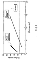
- FIG. 7 is a graph showing, in comparison with the prior art (the method shown in FIG. 10), an adhesive strength obtained on the basis of the method according to the embodiment of the present invention.
- the axis of abscissa indicates the area of a bonded part.
- the axis of ordinate indicates an adhesive strength.
- the present embodiment makes it possible to obtain a required adhesive strength (an adhesive strength of about 80 g or more, shown in the OK region) even with a very small bonded area compared to the prior art.
- each dummy land and the corresponding dummy through plug are connected together by thermo compression bonding using the metal material portion having a high adhesive strength. Consequently, a sufficient adhesive strength can be obtained even with a reduced bonded area. This enables a reduction in the area of each chip mounted substrate. It is thus possible to increase the number of chip mounted substrates that can be mounted on one chip-less substrate.
- the dummy land and dummy through plug can be formed between the areas in each of which the lands and through plugs proper are arranged, simultaneously with the formation of the lands and through plugs proper, using the same material as that of the lands and through plugs proper. Accordingly, the dummy land and the dummy through plug can be efficiently formed in terms of the positions and manufacturing process.
- an adhesive sheet (a sheet-like adhesive) 40 is located between each pair of unit substrates.
- a chip-less substrates 20a and 20b in which no device holes are formed are arranged in the uppermost and lowermost layers, respectively.
- the adhesive sheets 40 may be resin-based adhesives (for example, epoxy resin-based adhesives).
- the through plugs and the lands may be formed in only one of the chip-less substrates 20a and 20b.
- a plurality of the chip-less substrates 20a or 20b may be stacked on one another.
- each dummy through plug 17a is connected to the corresponding dummy land 23a so as to penetrate the adhesive sheet 40.
- Each land proper and the corresponding through plug proper which are different from the dummy land and the dummy through plug, respectively, are similarly connected together so as to penetrate the adhesive sheet 40.
- the unit substrates are bonded together via the adhesive sheets. This eliminates the need to apply an adhesive to both surfaces of each chip-less substrate before the formation of a device hole as in the case of the prior art. It is thus possible to improve the production efficiency and reliability of the stacked semiconductor device.
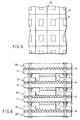
- the stacked substrate is cut along break lines 50 to divide the stacked substrate into areas in each of which a chip 12 is mounted, as shown in FIG. 5. This results in stacked semiconductor device having the plurality of chip mounted substrates 10 and chip-less substrates 20 stacked on one another as shown in FIG. 6.
- the metal material portion is provided in each part in which the dummy land and the dummy through plug are formed.
- the metal material portion may be provided in other parts as shown in the following variations.
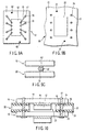
- FIGS. 8A to 8C show a first variation.
- FIG. 8A is a diagram showing the planar configuration of the chip mounted substrate 10.
- FIG. 8B is a diagram showing the planar configuration of the chip-less substrate 20.
- FIG. 8C is a diagram showing the sectional configuration of the vicinity of a bonded area of the bonded substrates.
- the basic configuration, bonding method, and the like of this variation are similar to those of the above described embodiment. Their description is thus omitted.
- dummy pads 61 are provided on the chip mounted substrate 10, while dummy pads 71 are provided on the chip-less substrate 20.
- the chip mounted substrate 10 and the chip-less substrate 20 are bonded together using metal material portions 31 each formed on at least one of the dummy pad 61 and the dummy pad 71.
- the metal material portions 31 are formed of a metal material such as solder, tin, or an Sn-Bi alloy which has a low melting point.
- the dummy pads 61 and 71 may be formed of a metal material such as copper.
- the present variation produces basic effects similar to those of the above described embodiment.
- the dummy pads can be arranged in arbitrary areas in arbitrary forms. This makes it possible to increase the degree of freedom of design.
- FIGS. 9A to 9C show a second variation.
- FIG. 9A is a diagram showing the planar configuration of the chip mounted substrate 10.
- FIG. 9B is a diagram showing the planar configuration of the chip-less substrate 20.
- FIG. 9C is a diagram showing the sectional configuration of the vicinity of a bonded area of the bonded substrates.
- the basic configuration, bonding method, and the like of this variation are similar to those of the above described embodiment. Their description is thus omitted.
- the present variation utilizes alignment marks 62 and 72 (formed of a metal material) for aligning the chip mounted substrate 10 and the chip-less substrate 20 with each other when they are stacked on each other.
- Each metal material portion 32 is formed on at least one of the alignment mark 62 and the alignment mark 72.
- the chip mounted substrate 10 and the chip-less substrate 20 are bonded together using the metal material portions 32.
- the metal material portions 32 are formed of a metal material such as solder, tin, or an Sn-Bi alloy which has a low melting point.
- the present variation produces basic effects similar to those of the above described embodiment. Moreover, the use of the alignment marks eliminates the need to provide dummy terminals or pads. This enables a further reduction in the size of each substrate and in the time required for the process.
- the chip mounted substrate and the chip-less substrate are bonded together using the metal material portions having a strong adhesive force. Consequently, a sufficient adhesive strength can be obtained even with a reduced bonded area. This enables a reduction in the size of each chip mounted substrate. It is thus possible to sharply increase the number of chip mounted substrates that can be mounted on the chip-less substrate.
- the unit substrates each formed of the chip mounted substrate and the chip-less substrate are bonded together using the adhesive sheets. This improves the production efficiency and reliability of the stacked substrates compared to the prior art.
Landscapes
- Engineering & Computer Science (AREA)
- Manufacturing & Machinery (AREA)
- Microelectronics & Electronic Packaging (AREA)
- Combinations Of Printed Boards (AREA)
- Production Of Multi-Layered Print Wiring Board (AREA)
- Wire Bonding (AREA)
- Testing Or Measuring Of Semiconductors Or The Like (AREA)
Abstract
Disclosed is a method of manufacturing a
semiconductor device, comprising preparing a first
substrate (10) including an integrated circuit chip
(12), first connection terminals electrically connected
to terminals of the integrated circuit chip, and a
first connection portion (16a, 17a) spaced from the
first connection terminals, preparing a second
substrate (20) including second connection terminals to
be electrically connected to the first connection
terminals and a second connection portion (23a, 24a)
spaced from the second connection terminals, providing
a metal material portion (30) for bonding on the first
connection portion or the second connection portion,
and stacking the first substrate and the second
substrate by connecting the first connection portion
and the second connection portion together via the
metal material portion by thermo compression bonding.
Description
The present invention relates to a semiconductor
device and a method of manufacturing a semiconductor
device, and in particular, to a technique to stack
substrates each having an integrated circuit chip.
In recent years, stacked semiconductor devices
have been proposed in each of which a plurality of
integrated circuit chips (LSI chips) are stacked on one
another.
FIG. 10 is a diagram showing a method of producing
such a stacked semiconductor device. This method
connects substrates 10 together on each of which an LSI
chip is mounted (such substrates will hereinafter be
referred to as chip mounted substrates), via
a substrate 20 on which no chips are mounted
(such a substrate will hereinafter be referred to as
a chip-less substrate). Usually, more chip mounted
substrates 10 and chip-less substrates 20 are stacked.
For simplification of description, the figure shows
only a part in which the two chip mounted substrates 10
and the one chip-less substrate 20 are stacked on one
another.
An LSI chip 12 is mounted on a substrate main
body 11 of the chip mounted substrate 10. External
terminals (not shown) of the LSI chip 12 are connected
to respective interconnects (not shown) provided on the
substrate main body 11 via anisotropic conductive
materials 14. The interconnects are connected to
respective lands 16 provided on the substrate main
body 11. The lands 16 are connected to respective
through plugs (via plugs) 17 penetrating the substrate
main body 11.
A plurality of the chip mounted substrates 10 are
mounted on the chip-less substrate 20. Openings
(device holes 22) are each formed in the chip-less
substrate 20 in association with an area of the chip
mounted substrate 10 in which the LSI chip 12 is
mounted. Furthermore, a substrate main body 21 of the
chip-less substrate 20 is formed with lands 23 and
through plugs (via plugs 24) penetrating the substrate
main body 21.
When the chip mounted substrates 10 and the
chip-less substrate 20 are stacked on one another, the
chip mounted substrates 10 and the chip-less substrate
20 are bonded together using a resin-based adhesive 29
applied to front and back surfaces of the chip-less
substrate 20.
In this manner, in the above described
conventional semiconductor device, the chip mounted
substrates 10 and the chip-less substrate 20 are bonded
together using the resin-based adhesive 29. However,
the resin-based adhesive 29 does not have a high
adhesive strength. Accordingly, a bonded area must be
enlarged in order to obtain a sufficient adhesive
strength. Disadvantageously, this unavoidably
increases the area of each chip mounted substrate 10,
preventing an increase in the number of chip mounted
substrates 10 that can be mounted on the one chip-less
substrate 20.
Furthermore, if the resin-based adhesive 29 is
applied after the formation of the device hole 22, the
device hole 22 may be filled with the adhesive 29 and
other problems may occur. Thus, the adhesive 29 is
applied to both surfaces of the substrate main body 21
of the chip-less substrate 20 before the formation of
the device holes 22. However, since the adhesive 29 is
applied to both surfaces of the substrate main body 21,
production efficiency may disadvantageously be
degraded. Furthermore, when the device holes 22 are
formed, the adhesive 29 may form flashes or the like.
This may degrade reliability.
As described above, in the prior art, the chip
mounted substrates and the chip-less substrate are
bonded together using the resin-based adhesive, which
does not have a strong adhesive force. Thus
disadvantageously, it is difficult to reduce the size
of each chip mounted substrate, and the number of chip
mounted substrates that can be mounted on the chip-less
substrate cannot be increased. Furthermore, in the
prior art, since the adhesive is applied to both
surfaces of the chip-less substrate before the
formation of the device holes, the production
efficiency and reliability may disadvantageously be
degraded.
It is an object of the present invention to
provide a semiconductor device and a method of
manufacturing a semiconductor device which can solve
the above described conventional problems.
A first aspect of the present invention is
a method of manufacturing a semiconductor device,
the method comprising: preparing a first substrate
including an integrated circuit chip, first connection
terminals electrically connected to terminals of the
integrated circuit chip, and a first connection portion
spaced from the first connection terminals; preparing a
second substrate including second connection terminals
to be electrically connected to the first connection
terminals and a second connection portion spaced from
the second connection terminals; providing a metal
material portion for bonding on the first connection
portion or the second connection portion; and stacking
the first substrate and the second substrate by
connecting the first connection portion and the second
connection portion together via the metal material
portion by thermo compression bonding.
A second aspect of the present invention is a
semiconductor device comprising: a first substrate
including an integrated circuit chip, first connection
terminals electrically connected to terminals of the
integrated circuit chip, and a first connection portion
spaced from the first connection terminals; a second
substrate stacked on the first substrate and including
second connection terminals and a second connection
portion spaced from the second connection terminals;
and a metal material portion provided between the first
connection portion and the second connection portion
and bonding the first connection portion to the second
connection portion.
A third aspect of the present invention is a
method of manufacturing a semiconductor device, the
method comprising: preparing a plurality of unit
substrates each comprising a first substrate and a
second substrate stacked, the first substrate including
an integrated circuit chip and first connection
terminals electrically connected to terminals of the
integrated circuit chip, the second substrate including
second connection terminals electrically connected to
the first connection terminals; and stacking the unit
substrates by bonding the unit substrates adjacent to
each other in a stacking direction using an adhesive
sheet.
A fourth aspect of the present invention is a
semiconductor device comprising: a plurality of unit
substrates each comprising a first substrate and a
second substrate stacked, the first substrate including
an integrated circuit chip and first connection
terminals electrically connected to terminals of the
integrated circuit chip, the second substrate including
second connection terminals electrically connected to
the first connection terminals; and an adhesive sheet
interposed between the unit substrates adjacent to each
other in a stacking direction and bonding the unit
substrates together.
With reference to the drawings, description will
be given below of a method of manufacturing a stacked
semiconductor device according to an embodiment of the
present invention.
FIG. 1A is a diagram schematically showing the
planar configuration of a chip mounted substrate 10.
FIG. 1B is a diagram schematically showing the
sectional configuration of the chip mounted substrate
10 along line B-B in FIG. 1A.
An LSI chip 12 is mounted on a substrate main body
11 of the chip mounted substrate 10 via an anisotropic
conductive material 14. External terminals 13 of the
LSI chip 12 are electrically connected to respective
interconnects 15 provided on the substrate main body 11
via the anisotropic conductive material 14. The
interconnects 15 are connected to respective lands 16
provided on the substrate main body 11. The lands 16
are electrically connected to respective through plugs
(via plugs) 17 penetrating the substrate main body 11.
The interconnects 15, the lands 16, and the through
plugs 17 are formed of a metal material such as copper
which has a low resistance. The lands 16 (through
plugs 17) have a pitch of, for example, 0.45 mm and a
diameter of, for example, 0.35 mm.
Pairs of a dummy land 16a and a dummy through plug
17a are each formed in a predetermined part between
connection terminals each composed of the land 16 and
the through plug 17, as a dummy terminal spaced from
the lands 16 and through plugs 17; that is, the dummy
terminal is not electrically connected to any external
terminals 13 of the LSI chip 12. The dummy lands 16a
and dummy through plugs 17a, and the lands 16 and
through plugs 17 proper, electrically connected to the
external terminal 13 of the LSI chip 12 can be
simultaneously formed of the same material.
A metal material portion 30 is formed on each of
the dummy lands 16a; the metal material portion is
formed of a metal material such as solder, tin, or an
Sn-Bi alloy which has a low melting point. The metal
material portions 30 are used to bond the chip mounted
substrate 10 to a chip-less substrate 20, described
later. The chip mounted substrate 10 and the chip-less
substrate 20 are bonded together by thermo compression
bonding so that the metal material portions 30 are
molten. Each of the metal material portions 30 has a
diameter of, for example, 0.2 mm and a thickness of,
for example, 0.75 mm or less (for example, 0.075 mm).
Normally, the metal material portion is similarly
formed on each of the lands 16 proper. However, in the
process described below, the metal material portions on
the lands 16 are not thermally molten.
The metal material portions 30 may be formed after
or before the LSI chip 12 is mounted. The distance
from each dummy land 16a to the adjacent land 16 is
preferably longer than the distance between the two
lands 16 so that upon thermo compression bonding, the
molten metal material portion 30 will not electrically
short-circuit the dummy land 16a and the adjacent land
16.
FIG. 2A is a diagram schematically showing the
planar configuration of the chip-less substrate 20.
FIG. 2B is a diagram schematically showing the
sectional configuration of the chip-less substrate 20
along line B-B in FIG. 2A.
A plurality of the chip mounted substrates 10,
shown in FIG. 1, are mounted on the chip-less
substrate 20. Openings (device holes 22) are each
formed in the chip-less substrate 20 in association
with an area of the chip mounted substrate 10 in which
the LSI chip 12 is mounted. Furthermore, a substrate
main body 21 of the chip-less substrate 20 is formed
with lands 23. The lands 23 are electrically connected
to respective through plugs (via plugs 24) penetrating
the substrate main body 21. The lands 23 and the
through plugs 24 are formed of a metal material such as
copper which has a low resistance. The lands 23 and
the through plugs 24 are arranged at positions
corresponding to the lands 16 and through plugs 17,
respectively, provided on the chip mounted
substrate 10.
Pairs of a dummy land 23a and a dummy through plug
24a are each formed in a predetermined part between
connection terminals each composed of the land 23 and
the through plug 23, as a dummy terminal spaced from
the lands 23 and through plugs 24. The dummy lands 23a
and dummy through plugs 24a and the lands 23 and
through plugs 24 proper can be simultaneously formed of
the same material. The dummy lands 23a and the dummy
through plugs 24a are arranged at positions
corresponding to the dummy lands 16a and dummy through
plugs 17a, respectively, provided in the chip mounted
substrate 10.
Then, as shown in FIG. 3, the chip mounted
substrate 10 and chip-less substrate 20, provided as
described above, are stacked on each other. The
substrates are stacked on each other by aligning the
substrates with each other and then using a thermo
compression bonding jig that can be heated to
selectively heat only the metal material portions 30 in
the respective areas in which the dummy land and the
dummy through plug are present, while contacting the
substrates with each other and pressing them against
each other. Conditions for the thermo compression
bonding include, for example, a temperature of 95°C and
a pressure of 0.5 MPa. As a result, the metal material
portion 30 is molten, and after the heating, the dummy
land 16a and the dummy through plug 24a are firmly
bonded together by the metal material portion 30.
In this case, by using ultrasonic wave together with
the heating as required, it is possible to reduce the
time required for the connection (for example, to about
two-thirds). In each of the parts in which the land
and through plug proper are present, which are
different from the dummy land and dummy through plug,
respectively, the metal material portion is not
thermally molten. Thus, the land and the through plug
are electrically connected together via the metal
material portion maintained in a solid state.
In the present example, the metal material portion
30 is formed on each of the dummy lands 16a of the chip
mounted substrate 10. However, the metal material
portion 30 may be formed on each of the dummy through
plugs 24a of the chip-less substrate 20. Furthermore,
each dummy land 16a and the corresponding dummy through
plug 17a of the chip mounted substrate 10 may be
reversely arranged in a vertical direction, whereas
each dummy land 23a and the corresponding dummy through
plug 24a of the chip-less substrate 20 may be reversely
arranged in the vertical direction. Then, the dummy
through plug 17a and the dummy land 23a may be
connected together via the metal material portion 30.
In this case, the dummy lands, dummy through plugs, and
metal material portion are connected together in the
order of 16a, 17a, 30, 23a, and 24a from the top to
bottom of FIG. 3. Also in this case, the metal
material portion 30 may be formed on the dummy through
plug 17a of the chip mounted substrate 10 or on the
dummy land 23a of the chip-less substrate 20.
Alternatively, the metal material portion 30 may be
formed on both dummy land and dummy through plug.
FIG. 7 is a graph showing, in comparison with the
prior art (the method shown in FIG. 10), an adhesive
strength obtained on the basis of the method according
to the embodiment of the present invention. The axis
of abscissa indicates the area of a bonded part.
The axis of ordinate indicates an adhesive strength.
As is apparent from this figure, the present embodiment
makes it possible to obtain a required adhesive
strength (an adhesive strength of about 80 g or more,
shown in the OK region) even with a very small bonded
area compared to the prior art.
In this manner, in the present embodiment, each
dummy land and the corresponding dummy through plug are
connected together by thermo compression bonding using
the metal material portion having a high adhesive
strength. Consequently, a sufficient adhesive strength
can be obtained even with a reduced bonded area. This
enables a reduction in the area of each chip mounted
substrate. It is thus possible to increase the number
of chip mounted substrates that can be mounted on one
chip-less substrate. Furthermore, the dummy land and
dummy through plug can be formed between the areas in
each of which the lands and through plugs proper are
arranged, simultaneously with the formation of the
lands and through plugs proper, using the same material
as that of the lands and through plugs proper.
Accordingly, the dummy land and the dummy through plug can be efficiently formed in terms of the positions and manufacturing process.
Accordingly, the dummy land and the dummy through plug can be efficiently formed in terms of the positions and manufacturing process.
Then, as shown in FIG. 4, in order to stack a
plurality of the unit substrates on one another, each
unit substrate comprising the chip mounted substrate 10
and the chip-less substrate 20 bonded together, an
adhesive sheet (a sheet-like adhesive) 40 is located
between each pair of unit substrates. A chip-less
substrates 20a and 20b in which no device holes are
formed are arranged in the uppermost and lowermost
layers, respectively. The adhesive sheets 40 may be
resin-based adhesives (for example, epoxy resin-based
adhesives). The through plugs and the lands may be
formed in only one of the chip-less substrates 20a and
20b. Alternatively, a plurality of the chip-less
substrates 20a or 20b may be stacked on one another.
After the unit substrates have been arranged as
shown in FIG. 4, they are pressurized in a stacking
direction so as to be bonded together using the
adhesive sheets 40. The adhesive sheets 40 are soft,
so that each dummy through plug 17a is connected to the
corresponding dummy land 23a so as to penetrate the
adhesive sheet 40. Each land proper and the
corresponding through plug proper, which are different
from the dummy land and the dummy through plug,
respectively, are similarly connected together so as to
penetrate the adhesive sheet 40.
In this manner, in the present embodiment, the
unit substrates are bonded together via the adhesive
sheets. This eliminates the need to apply an adhesive
to both surfaces of each chip-less substrate before the
formation of a device hole as in the case of the prior
art. It is thus possible to improve the production
efficiency and reliability of the stacked semiconductor
device.
After the plurality of unit substrates have been
stacked on one another, the stacked substrate is cut
along break lines 50 to divide the stacked substrate
into areas in each of which a chip 12 is mounted, as
shown in FIG. 5. This results in stacked semiconductor
device having the plurality of chip mounted substrates
10 and chip-less substrates 20 stacked on one another
as shown in FIG. 6.
In the above described embodiment, the metal
material portion is provided in each part in which the
dummy land and the dummy through plug are formed.
However, the metal material portion may be provided in
other parts as shown in the following variations.
FIGS. 8A to 8C show a first variation. FIG. 8A is
a diagram showing the planar configuration of the chip
mounted substrate 10. FIG. 8B is a diagram showing the
planar configuration of the chip-less substrate 20.
FIG. 8C is a diagram showing the sectional
configuration of the vicinity of a bonded area of the
bonded substrates. The basic configuration, bonding
method, and the like of this variation are similar to
those of the above described embodiment. Their
description is thus omitted.
In the present variation, dummy pads 61 are
provided on the chip mounted substrate 10, while dummy
pads 71 are provided on the chip-less substrate 20.
The chip mounted substrate 10 and the chip-less
substrate 20 are bonded together using metal material
portions 31 each formed on at least one of the dummy
pad 61 and the dummy pad 71. The metal material
portions 31 are formed of a metal material such as
solder, tin, or an Sn-Bi alloy which has a low melting
point. The dummy pads 61 and 71 may be formed of a
metal material such as copper.
The present variation produces basic effects
similar to those of the above described embodiment.
Moreover, the dummy pads can be arranged in arbitrary
areas in arbitrary forms. This makes it possible to
increase the degree of freedom of design.
FIGS. 9A to 9C show a second variation. FIG. 9A
is a diagram showing the planar configuration of the
chip mounted substrate 10. FIG. 9B is a diagram
showing the planar configuration of the chip-less
substrate 20. FIG. 9C is a diagram showing the
sectional configuration of the vicinity of a bonded
area of the bonded substrates. The basic
configuration, bonding method, and the like of this
variation are similar to those of the above described
embodiment. Their description is thus omitted.
The present variation utilizes alignment marks 62
and 72 (formed of a metal material) for aligning the
chip mounted substrate 10 and the chip-less substrate
20 with each other when they are stacked on each other.
Each metal material portion 32 is formed on at least
one of the alignment mark 62 and the alignment mark 72.
The chip mounted substrate 10 and the chip-less
substrate 20 are bonded together using the metal
material portions 32. The metal material portions 32
are formed of a metal material such as solder, tin, or
an Sn-Bi alloy which has a low melting point.
The present variation produces basic effects
similar to those of the above described embodiment.
Moreover, the use of the alignment marks eliminates the
need to provide dummy terminals or pads. This enables
a further reduction in the size of each substrate and
in the time required for the process.
As described above, according to the embodiments
of the present invention, the chip mounted substrate
and the chip-less substrate are bonded together using
the metal material portions having a strong adhesive
force. Consequently, a sufficient adhesive strength
can be obtained even with a reduced bonded area. This
enables a reduction in the size of each chip mounted
substrate. It is thus possible to sharply increase the
number of chip mounted substrates that can be mounted
on the chip-less substrate.
Furthermore, according to the embodiments of the
present invention, the unit substrates each formed of
the chip mounted substrate and the chip-less substrate
are bonded together using the adhesive sheets. This
improves the production efficiency and reliability of
the stacked substrates compared to the prior art.
According to the present invention, it is possible
to obtain an excellent stacked semiconductor device.
Claims (20)
- A method of manufacturing a semiconductor device, the method comprising:preparing a first substrate including an integrated circuit chip, first connection terminals electrically connected to terminals of the integrated circuit chip, and a first connection portion spaced from the first connection terminals;preparing a second substrate including second connection terminals to be electrically connected to the first connection terminals and a second connection portion spaced from the second connection terminals;providing a metal material portion for bonding on the first connection portion or the second connection portion; andstacking the first substrate and the second substrate by connecting the first connection portion and the second connection portion together via the metal material portion by thermo compression bonding.
- The method of manufacturing a semiconductor device according to claim 1, further comprising stacking unit substrates each formed of the first and second substrates stacked.
- The method of manufacturing a semiconductor device according to claim 2, wherein stacking the unit substrates includes bonding the unit substrates adjacent to each other in a stacking direction using an adhesive sheet.
- The method of manufacturing a semiconductor device according to claim 1, wherein the first connection portion is a first dummy terminal provided between the first connection terminals adjacent to each other in a plane direction, and the second connection portion is a second dummy terminal provided between the second connection terminals adjacent to each other in the plane direction.
- The method of manufacturing a semiconductor device according to claim 1, wherein the first connection portion is a first dummy pad provided on the first substrate, and the second connection portion is a second dummy pad provided on the second substrate.
- The method of manufacturing a semiconductor device according to claim 1, wherein the first connection portion is a first alignment mark provided on the first substrate and used to align the first substrate with the second substrate, and the second connection portion is a second alignment mark provided on the second substrate and used to align the first substrate with the second substrate.
- The method of manufacturing a semiconductor device according to claim 1, wherein the metal material portion is formed of solder, tin, or an Sn-Bi alloy.
- The method of manufacturing a semiconductor device according to claim 3, wherein the adhesive sheet is formed of resin.
- A semiconductor device comprising:a first substrate including an integrated circuit chip, first connection terminals electrically connected to terminals of the integrated circuit chip, and a first connection portion spaced from the first connection terminals;a second substrate stacked on the first substrate and including second connection terminals and a second connection portion spaced from the second connection terminals; anda metal material portion provided between the first connection portion and the second connection portion and bonding the first connection portion to the second connection portion.
- The semiconductor device according to claim 9, wherein a plurality of unit substrates are stacked, each of the unit substrates being formed of the first and second substrates stacked.
- The semiconductor device according to claim 10, further comprising an adhesive sheet interposed between the unit substrates adjacent to each other in a stacking direction and bonding the unit substrates together.
- The semiconductor device according to claim 9, wherein the first connection portion is a first dummy terminal provided between the first connection terminals adjacent to each other in a plane direction, and the second connection portion is a second dummy terminal provided between the second connection terminals adjacent to each other in the plane direction.
- The semiconductor device according to claim 9, wherein the first connection portion is a first dummy pad provided on the first substrate, and the second connection portion is a second dummy pad provided on the second substrate.
- The semiconductor device according to claim 9, wherein the first connection portion is a first alignment mark provided on the first substrate and used to align the first substrate with the second substrate, and the second connection portion is a second alignment mark provided on the second substrate and used to align the first substrate with the second substrate.
- The semiconductor device according to claim 9, wherein the metal material portion is formed of solder, tin, or an Sn-Bi alloy.
- The semiconductor device according to claim 11, wherein the adhesive sheet is formed of resin.
- A method of manufacturing a semiconductor device, the method comprising:preparing a plurality of unit substrates each comprising a first substrate and a second substrate stacked, the first substrate including an integrated circuit chip and first connection terminals electrically connected to terminals of the integrated circuit chip, the second substrate including second connection terminals electrically connected to the first connection terminals; andstacking the unit substrates by bonding the unit substrates adjacent to each other in a stacking direction using an adhesive sheet.
- The method of manufacturing a semiconductor device according to claim 17, wherein the adhesive sheet is formed of resin.
- A semiconductor device comprising:a plurality of unit substrates each comprising a first substrate and a second substrate stacked, the first substrate including an integrated circuit chip and first connection terminals electrically connected to terminals of the integrated circuit chip, the second substrate including second connection terminals electrically connected to the first connection terminals; andan adhesive sheet interposed between the unit substrates adjacent to each other in a stacking direction and bonding the unit substrates together.
- The semiconductor device according to claim 19, wherein the adhesive sheet is formed of resin.
Applications Claiming Priority (3)
| Application Number | Priority Date | Filing Date | Title |
|---|---|---|---|
| JP2001304745A JP2003110091A (en) | 2001-09-28 | 2001-09-28 | Semiconductor device and method of manufacturing semiconductor device |
| JP2001304745 | 2001-09-28 | ||
| PCT/JP2002/009826 WO2003030260A1 (en) | 2001-09-28 | 2002-09-25 | Semiconductor device and semiconductor device manufacturing method |
Publications (2)
| Publication Number | Publication Date |
|---|---|
| EP1432034A1 true EP1432034A1 (en) | 2004-06-23 |
| EP1432034A4 EP1432034A4 (en) | 2007-12-12 |
Family
ID=19124623
Family Applications (1)
| Application Number | Title | Priority Date | Filing Date |
|---|---|---|---|
| EP02772899A Withdrawn EP1432034A4 (en) | 2001-09-28 | 2002-09-25 | SEMICONDUCTOR DEVICE AND METHOD FOR PRODUCING THE SAME |
Country Status (7)
| Country | Link |
|---|---|
| US (1) | US7141872B2 (en) |
| EP (1) | EP1432034A4 (en) |
| JP (1) | JP2003110091A (en) |
| KR (1) | KR100628418B1 (en) |
| CN (1) | CN100382312C (en) |
| TW (1) | TW571434B (en) |
| WO (1) | WO2003030260A1 (en) |
Families Citing this family (10)
| Publication number | Priority date | Publication date | Assignee | Title |
|---|---|---|---|---|
| JP2006165320A (en) * | 2004-12-08 | 2006-06-22 | Matsushita Electric Ind Co Ltd | Semiconductor laminated module and manufacturing method thereof |
| JP4504798B2 (en) * | 2004-12-16 | 2010-07-14 | パナソニック株式会社 | Multistage semiconductor module |
| JP4356683B2 (en) * | 2005-01-25 | 2009-11-04 | セイコーエプソン株式会社 | Device mounting structure and device mounting method, droplet discharge head and connector, and semiconductor device |
| JP4520355B2 (en) * | 2005-04-19 | 2010-08-04 | パナソニック株式会社 | Semiconductor module |
| JP2007317861A (en) * | 2006-05-25 | 2007-12-06 | Nec Lcd Technologies Ltd | Multilayer printed circuit board and liquid crystal display device |
| KR101563630B1 (en) * | 2009-09-17 | 2015-10-28 | 에스케이하이닉스 주식회사 | Semiconductor package |
| JP5887901B2 (en) * | 2011-12-14 | 2016-03-16 | 富士電機株式会社 | Semiconductor device and manufacturing method of semiconductor device |
| EP3104410B1 (en) * | 2014-03-10 | 2022-12-07 | Mitsubishi Heavy Industries, Ltd. | Multi-chip module, on-board computer, sensor interface substrate, and multi-chip module manufacturing method |
| US9659985B2 (en) * | 2015-02-17 | 2017-05-23 | Taiwan Semiconductor Manufacturing Company Ltd. | Integrated circuit and image sensing device having metal shielding layer and related fabricating method |
| JP7242342B2 (en) | 2019-02-22 | 2023-03-20 | 三菱重工業株式会社 | Multichip module, electronic device and method of manufacturing multichip module |
Family Cites Families (14)
| Publication number | Priority date | Publication date | Assignee | Title |
|---|---|---|---|---|
| JPS61127153A (en) * | 1984-11-26 | 1986-06-14 | Matsushita Electric Works Ltd | Mounting structure for semiconductor element |
| US5239448A (en) * | 1991-10-28 | 1993-08-24 | International Business Machines Corporation | Formulation of multichip modules |
| JPH07106509A (en) * | 1993-09-29 | 1995-04-21 | Nitto Denko Corp | Multi-layer semiconductor device |
| US5454160A (en) * | 1993-12-03 | 1995-10-03 | Ncr Corporation | Apparatus and method for stacking integrated circuit devices |
| US6020629A (en) * | 1998-06-05 | 2000-02-01 | Micron Technology, Inc. | Stacked semiconductor package and method of fabrication |
| US6376769B1 (en) * | 1999-05-18 | 2002-04-23 | Amerasia International Technology, Inc. | High-density electronic package, and method for making same |
| TW472330B (en) * | 1999-08-26 | 2002-01-11 | Toshiba Corp | Semiconductor device and the manufacturing method thereof |
| JP2001177051A (en) * | 1999-12-20 | 2001-06-29 | Toshiba Corp | Semiconductor device and system device |
| JP2001230365A (en) * | 2000-02-15 | 2001-08-24 | Sony Corp | Multilayer semiconductor device and method of manufacturing the same |
| JP2001339043A (en) * | 2000-05-30 | 2001-12-07 | Mitsubishi Electric Corp | Semiconductor device and semiconductor module using the same |
| US6404043B1 (en) * | 2000-06-21 | 2002-06-11 | Dense-Pac Microsystems, Inc. | Panel stacking of BGA devices to form three-dimensional modules |
| US6577013B1 (en) * | 2000-09-05 | 2003-06-10 | Amkor Technology, Inc. | Chip size semiconductor packages with stacked dies |
| JP2002176137A (en) * | 2000-09-28 | 2002-06-21 | Toshiba Corp | Stacked semiconductor device |
| JP3655242B2 (en) * | 2002-01-04 | 2005-06-02 | 株式会社東芝 | Semiconductor package and semiconductor mounting apparatus |
-
2001
- 2001-09-28 JP JP2001304745A patent/JP2003110091A/en active Pending
-
2002
- 2002-09-24 TW TW091121902A patent/TW571434B/en not_active IP Right Cessation
- 2002-09-25 WO PCT/JP2002/009826 patent/WO2003030260A1/en not_active Ceased
- 2002-09-25 KR KR1020047004575A patent/KR100628418B1/en not_active Expired - Fee Related
- 2002-09-25 CN CNB028189604A patent/CN100382312C/en not_active Expired - Fee Related
- 2002-09-25 EP EP02772899A patent/EP1432034A4/en not_active Withdrawn
-
2004
- 2004-03-24 US US10/807,311 patent/US7141872B2/en not_active Expired - Fee Related
Also Published As
| Publication number | Publication date |
|---|---|
| CN1559088A (en) | 2004-12-29 |
| TW571434B (en) | 2004-01-11 |
| KR20040045017A (en) | 2004-05-31 |
| WO2003030260A1 (en) | 2003-04-10 |
| US7141872B2 (en) | 2006-11-28 |
| EP1432034A4 (en) | 2007-12-12 |
| KR100628418B1 (en) | 2006-09-28 |
| US20040238935A1 (en) | 2004-12-02 |
| JP2003110091A (en) | 2003-04-11 |
| CN100382312C (en) | 2008-04-16 |
Similar Documents
| Publication | Publication Date | Title |
|---|---|---|
| US10765006B2 (en) | Electronic module | |
| CN100356510C (en) | Semiconductor device and manufacturing method for the same | |
| US6025648A (en) | Shock resistant semiconductor device and method for producing same | |
| KR100523495B1 (en) | Semiconductor device and fabrication method thereof | |
| TW512498B (en) | Semiconductor device, method of manufacture thereof, circuit board, and electronic device | |
| US7768119B2 (en) | Carrier structure embedded with semiconductor chip | |
| EP1372193B1 (en) | Method of manufacturing a semiconductor device having a stacked configuration | |
| KR20080037740A (en) | A microfeature assembly comprising an interconnect structure and a method of forming the interconnect structure | |
| DE102010000407B4 (en) | A semiconductor package comprising a metal layer tape and method of making such a semiconductor package | |
| KR100335454B1 (en) | Multilayered circuit board for semiconductor chip module, and method of manufacturing the same | |
| US20090014852A1 (en) | Flip-Chip Packaging with Stud Bumps | |
| CN105789173B (en) | Circuit board integrating interposer and dual wiring structure and manufacturing method thereof | |
| JP2005167244A (en) | Thin package used for integrated circuit stacking | |
| US7141872B2 (en) | Semiconductor device and method of manufacturing semiconductor device | |
| CN102047402B (en) | A kind of electronic device manufacturing method | |
| CN112714539A (en) | Electronic component and method of manufacturing an electronic component | |
| JPH10335528A (en) | Semiconductor package and method of manufacturing semiconductor package | |
| US9536857B1 (en) | Heating header of semiconductor mounting apparatus and bonding method for semiconductor | |
| JP3163075B2 (en) | Wiring board with metal stiffener | |
| JP2001168232A (en) | Circuit component connected body, method for manufacturing circuit component connected body, double-sided circuit board, method for manufacturing double-sided circuit board, circuit component mounted body, and multilayer circuit board | |
| JP2007115789A (en) | Stacked semiconductor device and method for manufacturing stacked semiconductor device | |
| EP1317001A1 (en) | A semiconductor device | |
| JPH06334059A (en) | Semiconductor mounting board and production thereof | |
| JP2001035997A (en) | Semiconductor device and manufacturing method thereof | |
| JP2000012724A (en) | Circuit board for bare chip mounting |
Legal Events
| Date | Code | Title | Description |
|---|---|---|---|
| PUAI | Public reference made under article 153(3) epc to a published international application that has entered the european phase |
Free format text: ORIGINAL CODE: 0009012 |
|
| 17P | Request for examination filed |
Effective date: 20040319 |
|
| AK | Designated contracting states |
Kind code of ref document: A1 Designated state(s): DE FR GB |
|
| AX | Request for extension of the european patent |
Extension state: AL LT LV MK RO SI |
|
| RIN1 | Information on inventor provided before grant (corrected) |
Inventor name: YOSHIMURA, ATSUSHI |
|
| A4 | Supplementary search report drawn up and despatched |
Effective date: 20071112 |
|
| 17Q | First examination report despatched |
Effective date: 20100708 |
|
| STAA | Information on the status of an ep patent application or granted ep patent |
Free format text: STATUS: THE APPLICATION IS DEEMED TO BE WITHDRAWN |
|
| 18D | Application deemed to be withdrawn |
Effective date: 20101119 |